Tests as Run
DOCUMENT SCOPE
The aim of this document is to clearly explain the tests performed during the delevolpment of the subsystem.
This document is based on current but also previous versions both of hardware and software and as such be followed with care.
TEST 1: Electrical check
Test Description and Objectives
The aim of this test is to verify that non of the components or connections had been damaging during the assembling, and that the consumption of the components is nominal.
Requirements Verification
| Requirement ID | Description |
|---|---|
| OBC-001 | There must be no visible damage to the board, such as scratches, soldering or joint issues. |
| OBC-011 | Each pin found in the lateral sides must have good electrical connection |
| OBC-012 | Verify that there are not any shorts, nor open ends, and the corresponding behavior and value |
| OBC-021 | The board must be powered with 3.3 V and all the power pins from the board must be checked |
| OBC-031 | All the other pins from the board must be electrically checked in order to make sure that the board is responding correctly |
Test Set-Up
- OBC payload full soldered
- Microscope
- Power Supply
- Wires
- Soldering machine
- Tin
- Flux
- Multi-meter
- Calculator, pen and paper
- Laptop with KiCad and the design
Pass/Fail Criteria
The PCB will be verified if the five requirements mentioned before are fulfilled. If in one of them it is detected any anomaly it will have to be corrected, otherwise the board can not pass to the other tests.
Test Plan
- With the help of the microscope, look at the PCB looking for any outer physical parameters, such as scratches, soldering or joint issues. If any anomaly is detected, re-solder or fix the encountered error.
- Check the correct connection with the corresponding component of the 40 pins (10 in each lateral side) with the multi-meter.
- Check the value with the multi-meter of all the passive components and compare it to the one in the schematic.
- Verify the active components, checking one by one all the pins with the multi-meter in order to find shorts, open ends, and correct connections among the various pins.
- Check the connections between all of the components and pins of the PCB
Test Results
The test for the EPS PCB has been done during the 01/06/2023.
The test passed the visual inspection since the outer physical checking was successful.
The pins', passive and active components' connectivity were successfully accomplished considering that there were no open ends or shorts, and the component values were correct.
The in-circuit testing was passed since the connections between all of the components and pints of the PCB were verified.
Anomalies
During the examination of the PCB no anomalies were detected.
Conclusions
The PCB passed the electrical test and is ready to do more complex tests.
TEST 2: In-circuit voltages
Test Description and Objectives
The objective of this test is to verify that when providing the PCB with the power supply, the voltages and currents are correct on the whole PCB
Requirements Verification
The voltages required for each component are summarized in the following chart (they can be seen from the datasheet of each component):
| COMPONENT | Vin Min (V) | Vin Max (V) | Vo Min (V) | Vo Max(V) |
| SX1262IMLTRT | 1.8 | 3.7 | - | - |
| BGS12PL6E6327XTSA1 | 1.65 | 3.6 | - | - |
| STM32L476RGTx | 1.71 | 3.6 | - | - |
| BD2232G-GTR | 2.7 | 5.5 | -0.3 | Vin + 0.3 |
Test Set-Up
- OBC payload
- Microscope
- Multimeter
- Power supply unit
- Wires
- Pen and paper
- Computer with KiCad and the design
Pass/Fail Criteria
This test will be verified if the voltage obtained in the measurements of each component of the PCB is between the expected values.
Test Plan
- Prepare the power supply with 3.3V
- Connect the power supply to the PCB (3V3_PERM and GND)

- With the help of the multimeter, check that the inputs pins has the 3.3V value

With the help of the multimeter, check the voltage levels in the input and output of each component of the 3.2 chart
(the previous mentioned components are shown in order in the figures below, where the input put are marked in red)


Test Results
This test for the EPS PCB has been done during the 01/06/2023.
| COMPONENT | Vin (V) |
| SX1262IMLTRT | 3.35 |
| BGS12PL6E6327XTSA1 | 3.32 |
| STM32L476RGTx | 3.27 |
| BD2232G-GTR | 3.34 |
As it can be seen in the previous chart, all the components have the correct input voltage. The test has been correctly passed.
Anomalies
No anomalies has been detected
Conclusions
The PCB passed the test and is ready to do more complex tests.
TEST 3: STM32L476RG Flashing
Test Description and Objectives
The objective of this test is to verify that it is possible to flash code to the STM32L476RG using the ST-Link v2
Requirements Verification
| Requirement ID | Description |
|---|---|
|
OBC-101 |
The program ST-Link Utility must detect the STM32L476RG |
|
OBC-111 |
The STM32 must be able to run code |
|
OBC-121 |
A very simple instruction with a visible result must be written in order to prove that the code works correctly |
Test Set-Up
- OBC payload
- Microscope
- Multimeter
- ST-Link V2
- Saleae
- Wires
- Pen and paper
- Computer with KiCad, ST-Link Utility and Saleae
Pass/Fail Criteria
This test will be verified if the two requirements are fullfiled.
Test Plan
- Connect the ST-Link V2 to the OBC board


- Open the ST-Link utility program
- Connect the ST-Link V2 to the PC
- Click in the connection option and check if the program detects the STM32L476RG
- Open the STM32CubeIDE
- Debug code to see if the program detects the STM32L476RG
- Flash code


4.5.1 Debbuging steps for STM32 SWD Connection
ST-Link V2 connected to PC?
Yes
Connections ok? Revise ST-Link V2 and STM32 custom board SWD connections
Connection ok** **
**

STM32CubeIDE debbuger configured ok?

Supply ok? Check voltages
- Power Supply: 3.3V ok
- VCC PIN 1 STM: 3.3V ok
- VCC PIN 13 STM: 3.3V ok
- VCC PIN 19 STM: 3.3V ok
- VCC PIN 32 STM: 3.3V ok
- VCC PIN 48 STM: 3.3V ok
- VCC PIN 64 STM: 3.3V ok
ST-Link V2 ok? Try programming Nucleo board with ST-Link V2d
STM32 detects the nucleo board. Therefore, the ST_Link v2 is ok.

Signals and logic ok? Connect Saleae to SWD and NRST in STM32 custom board
The SWDO and the SWCLK are working ok, but no signal is received from the NRST PIN. The same happens when the Saleae is connected directly to the STM32.
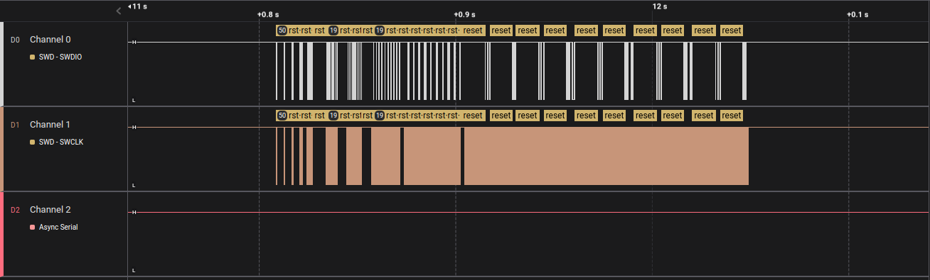
Signals from ST-Link V2 ok? Connect Saleae to SWD and NRST in ST-Link V2. Check if NRST is being aserted
Prepare STM32 board with minimum connections, only supply, gnd and SWD, does it work?
No, the ST-Link still does not detect the STM32
Resolder the board
When resoldering the board a mistake was detected: The STM32 has two orientation marks, and it was placed in the wrong direction. It is important to know that the hole that indicates the direction of the STM32 is the small one:

With the STM32 well orientated and the new PCB resoldered, the ST-Link can now make a connection with the STM32L476RG and flash code into it.
Test Results
This test for the OBC PCB has been done during the 02/06/2023.
The STM32L476RG was succesfully detected by the ST-Link Utility program

The STM32CubeIde also detected the STM32 and was able to run code through it.

Anomalies
When trying to do the connection with the ST-Link utility program, the STM32 was no detected. The debugging process realized to solve this problem can be seen in 4.5.1.
Conclusions
The PCB passed the test.
TEST 4: STM32L476RG functional test
Test Description and Objectives
The aim of this test is to verify that the required functions of the OBC can be performed by the STM32L4 integrated.
Requirements Verification
| Requirement ID | Description |
|---|---|
|
OBC - 211 |
The peripherals must be able to be correctly initialized |
|
OBC - 212 |
The clock has been able to be configured |
|
OBC - 221 |
FreeRTOS must be able to create a task |
|
OBC - 222 |
FreeRTOS must be able to do task scheduling |
|
OBC - 223 |
FreeRTOS must be able to make queue inter-tasks communication |
|
OBC - 224 |
It is needed to write on memory flash |
|
OBC - 225 |
The clock configuration can be changed during run-time |
|
OBC - 231 |
Be able to do software timers triggering (in 80, 26, 8 and 2 MHz) |
Test Set-Up
- OBC payload
- ST-Link V2
- Wires
- Pen and paper
- Computer with KiCad, ST-Link Utility and Saleae
- STM32CubeIDE with OBC code
Pass/Fail Criteria
The PCB will be verified if the five requirements mentioned before are fulfilled. If in one of them it is detected any anomaly it will have to be corrected, otherwise the board can not pass to the other tests.
Test Plan
- Connect the OBC to the ST-Link using the SWDIO connection
- Connect the ST-Link to the computer
- Run the code, implemented by Nil Rius, for the OBC
- Verify the correct initialization of the peripherals and the clock
- Check the task management list provided by FreeRTOS in order to verify the correct task creation and management.
- Use the FreeRTOS' functions to write in memory and look in the memory map to veirfy the correct writing.
- Verify that when the code changes the frequency of the clocks, the timer triggers at the correct time
Test Results
The test for the OBC PCB has been done during the 10/06/2023.
All the requirements have been successfully met.
Anomalies
During the examination of the PCB no anomalies were detected.
Conclusions
The PCB passed the STM32 functional test.
TEST 5: I2C reading of Temperature Sensor data test
Test Description and Objectives
This test is designed to attempt communication from the OBC-COMMS board, via I2C, to the TCN75A temperature sensor located on all of the lateral boards.
Requirements Verification
| Requirement ID | Description |
|---|---|
|
OBC-311 |
The sensor must be powered using the Nucleo board's output. |
|
OBC-312 |
Using the Nucleo, the configuration register of the temperature sensor must be set (TX). |
|
OBC-313 |
Using the Nucleo, the temperature data from the sensor must be received and tracked using PuTTY for a cleaner reading of the data (RX). |
|
OBC-321 |
The sensor must be powered using the output from the ST-Link/V2 programmer. |
|
OBC-322 |
The already written and tested code from the Nucleo must be correctly flashed onto the OBC-COMMS board using the ST-Link/V2 programmer. |
|
OBC-323 |
Using the OBC-COMMS board, the configuration register of the sensor must be set (TX). |
|
OBC-324 |
Using the OBC-COMMS board, the temperature data from the sensor must be received (RX). |
|
OBC-331 |
The temperature reading function must be defined and integrated in the main code from GitHub. |
|
OBC-332 |
The complete GitHub code, including the newly written function, must be flashed onto the OBC-COMMS board using the ST-Link/V2 programmer. |
|
OBC-333 |
Using the already flashed OBC-COMMS board, it must be shown that the configuration and temperature data is still being sent and received through I2C when the previously integrated function is called in the main(). |
Test Setup
Necessary materials:
- Lateral board with the TCN75A temperature sensor and all the necessary components (as seen in the KiCad project);
- Nucleo-L476RG board;
- OBC-COMMS board;
- ST-Link/V2 programmer;
- 2 x 4.7k Ω resistors (for pull-up);
- USB - USB 2.0 cable;
- 10 pin Molex connector and 4 crimped cables;
- Normal F-M and M-M cables;
- Protoboard;
- Laptop with STM32CubeIDE, KiCad, PuTTY and Picoscope installed and at least one USB port;
- Multimeter and oscilloscope/Picoscope for testing.
The setup for the initial test with the Nucleo:

[Detailed schematic made in photoshop to be inserted at a later date]
The setup for the subsequent test with the OBC-COMMS board:

[Detailed schematic made in photoshop to be inserted at a later date]
Pass/Fail Criteria
All of the requirements mentioned before must be fulfilled. If any one of them is not satisfactorily carried out, the anomalies must be taken care of. This test is absolutely critical since this is the easiest peripheral for I2C communication testing and this protocol is used for most internal communication jobs, so it is mandatory that it works without a hitch.
Test Plan
6.5.1. Initial test with the Nucleo board
Step 1:
Build the previously shown setup. Make sure all of the connections are good and, using the multimeter, measure all of the relevant voltages (Power Pin, NRST, SWDIO, SWCLK, I2C SDA, I2C SCL) to make sure they reach around 3.3 V.
Step 2:
All code and software related stuff will be done in STM32CubeIDE, as it's the easiest and most reliable tools to use.
Write code for transmitting configuration settings to the configuration register of the sensor (thus testing TX) and receiving temperature data from the temperature register of the sensor (thus also testing RX).
Make sure you read the documentation data for the TCN75A sensor in particular, how it handles I2C communication and pay special attention to the way the address of the sensor is formatted, taking into account the particular configuration of resistors from the lateral board which define the last 3 bits of said address.
Step 3:
Flash the Nucleo board with the code you have written (look-up tutorial), open PuTTY, put in the parameters of your serial virtual COM port which gets created automatically from the Nucleo debugger (you can see it in Device Manager -> Port) and connect. Run the program and see if the data gets transmitted correctly. You can touch the sensor to warm it up and check if the temperature readings match.
Optional:
You can check the I2C SDA and SCL signals respectively with the oscilloscope/Picoscope you're using.
The Picoscope IDE also allows you to decode the 2 signals if both are connected, which should technically give you the same output as in PuTTY.
6.5.2. OBC-COMMS board test
Once you have made sure that you can communicate through I2C between the Nucleo board and the sensor, it's time to try it with the main OBC-COMMS board.
The steps you should follow are exactly the same:
Step 1:
Build the previously shown setup.
Step 2 (extremely important):
Create a new project and redo the pin configuration in order to match the KiCad project for the OBC-COMMS board.
In particular, the I2C pins are not PB8 and PB9, but PB6 and PB7.
The code until and including the main() can be copy-pasted in its entirety from the other project.
Step 3:
Flash the code from this new project on the OBC-COMMS board using the debugger and test the values for the relevant variables while debugging. Since the ST-Link/V2 does not create a virtual COM port, the easiest way to check if the I2C communication is correctly being performed is by debugging step by step and checking if the variables change according to how they're supposed to.
6.5.3. Temperature reading function definition, integration and testing with the full code
Now that the OBC-COMMS -> Temperature Sensor communication works, the only thing left to do is to create a function, integrate it in the full code and test its functionality as a whole.
One of the ways to do this is:
Step 1:
Decide in what subsystem you want to integrate this code. In this case, it would make the most sense to write a function in the ADCS subsystem, since everything related to the lateral board "depends" on the ADCS.
Step 2:
Write the function and its corresponding header. Make sure to include everything you need in the header, especially all files which contain the I2C functions.
The .c file will be basically the same as the other code, containing all the functions that the other one contains, and changing it so that the main() of the existing code is all contained inside a function that will be called in the main.c file in order to test if everything works as intended.
Step 3:
Call the previously brought up function in the main.c file of the program.
Repeat the setup from the previous test and flash the entire code on the OBC-COMMS board. While debugging, go step by step and when you reach the temperature sensor data reading function, click on "Step into", and again, go step by step and check the relevant variables to see if their values correspond with your expected outputs.
If everything is good and nothing in the code crashed unexpectedly, that means that the integration test was successful.
Test Results
6.6.1. Initial test with the Nucleo board
This is the code I wrote for the Nucleo board test (not including the autogenerated functions):
//* Includes ------------------------------------------------------------------*/
#include "main.h"
#include "i2c.h"
/* Private includes ----------------------------------------------------------/
#include <string.h>
#include <stdio.h>
#include <math.h>
/ Private typedef -----------------------------------------------------------/
/ USER CODE BEGIN PTD /
/ USER CODE END PTD */
/* Private define ------------------------------------------------------------*/
#define TCN75_ADDR 0x4C // Change as per your hardware configuration
#define REG_CONFIG 0x01
#define REG_TEMP 0x00
/* USER CODE BEGIN PD /
/ USER CODE END PD */
/* Private macro -------------------------------------------------------------/
/ USER CODE BEGIN PM /
/ USER CODE END PM */
/* Private variables ---------------------------------------------------------*/
I2C_HandleTypeDef hi2c1;
UART_HandleTypeDef huart2;
/* USER CODE BEGIN PV /
/ USER CODE END PV */
/* Private function prototypes -----------------------------------------------*/
void SystemClock_Config(void);
static void MX_GPIO_Init(void);
static void MX_USART2_UART_Init(void);
void MX_I2C1_Init(void);
/* USER CODE BEGIN PFP */
void I2C_ReInit(void);
HAL_StatusTypeDef I2C_CheckError(I2C_HandleTypeDef *hi2c, uint16_t DevAddress);
void I2C_BusReset(void);
void UART_Log(char message);
/ USER CODE END PFP */
/* USER CODE BEGIN 0 */
void I2C_ReInit(void) {
HAL_I2C_DeInit(&hi2c1);
MX_I2C1_Init();
}
HAL_StatusTypeDef I2C_CheckError(I2C_HandleTypeDef *hi2c, uint16_t DevAddress) {
if (HAL_I2C_IsDeviceReady(hi2c, DevAddress, 3, 1000) != HAL_OK) {
uint32_t errorCode = HAL_I2C_GetError(hi2c);
char errorMsg[64];
sprintf(errorMsg, "I2C Error: 0x%lx\r\n", errorCode);
UART_Log(errorMsg);
I2C_ReInit();
return HAL_ERROR;
}
return HAL_OK;
}
void I2C_BusReset(void) {
GPIO_InitTypeDef GPIO_InitStruct = {0};
HAL_I2C_DeInit(&hi2c1);
GPIO_InitStruct.Pin = GPIO_PIN_9 | GPIO_PIN_8;
GPIO_InitStruct.Mode = GPIO_MODE_OUTPUT_OD;
GPIO_InitStruct.Pull = GPIO_NOPULL;
GPIO_InitStruct.Speed = GPIO_SPEED_FREQ_HIGH;
HAL_GPIO_Init(GPIOB, &GPIO_InitStruct);
for (int i = 0; i < 9; i++) {
HAL_GPIO_WritePin(GPIOB, GPIO_PIN_8, GPIO_PIN_SET);
HAL_Delay(1);
HAL_GPIO_WritePin(GPIOB, GPIO_PIN_8, GPIO_PIN_RESET);
HAL_Delay(1);
}
MX_I2C1_Init();
}
void UART_Log(char message) {
HAL_UART_Transmit(&huart2, (uint8_t)message, strlen(message), HAL_MAX_DELAY);
}
int main(void) {
HAL_Init();
SystemClock_Config();
MX_GPIO_Init();
MX_USART2_UART_Init();
MX_I2C1_Init();
while (1) {
uint8_t buf[12];
int8_t val_bfc;
float val_afc = 0.0f;
uint8_t auxbuf[12];
char sign = ' ';
buf[0] = REG_CONFIG;
buf[1] = 0x60; // Example configuration value
char AuxilMsg[64];
sprintf(AuxilMsg, "While loop reset \r\n");
HAL_UART_Transmit(&huart2, AuxilMsg , strlen(AuxilMsg), HAL_MAX_DELAY);
if (I2C_CheckError(&hi2c1, TCN75_ADDR << 1) == HAL_OK) {
sprintf(AuxilMsg, "I2C OK \r\n");
HAL_UART_Transmit(&huart2, AuxilMsg , strlen(AuxilMsg), HAL_MAX_DELAY);
HAL_I2C_Master_Transmit(&hi2c1, TCN75_ADDR << 1, buf, 2, HAL_MAX_DELAY);
buf[0] = REG_TEMP;
sprintf(AuxilMsg, "First transmission complete \r\n");
HAL_UART_Transmit(&huart2, AuxilMsg , strlen(AuxilMsg), HAL_MAX_DELAY);
HAL_I2C_Master_Transmit(&hi2c1, TCN75_ADDR << 1, buf, 1, HAL_MAX_DELAY);
sprintf(AuxilMsg, "Second transmission complete \r\n");
HAL_UART_Transmit(&huart2, AuxilMsg , strlen(AuxilMsg), HAL_MAX_DELAY);
HAL_I2C_Master_Receive(&hi2c1, (TCN75_ADDR << 1) | 0x01, buf, 2, HAL_MAX_DELAY);
sprintf(AuxilMsg, "Receiving complete \r\n");
HAL_UART_Transmit(&huart2, AuxilMsg , strlen(AuxilMsg), HAL_MAX_DELAY);
if(buf[0] >= 0x80)
{sign = '-';
auxbuf[0] = buf[0] - 0x80;
auxbuf[1] = buf[1];
}
else
{
auxbuf[0] = buf[0];
auxbuf[1] = buf[1];
}
val_bfc = (uint8_t) auxbuf[0];
for (int i = 0; i < 8; ++i) {
if (auxbuf[1] & (1 << i)) {
val_afc += 1 / pow(2, 8-i);
}
}
val_afc *= 100;
char tempMsg[64];
sprintf(tempMsg, "Temperature: %c%d.%02d C\r\n", sign, val_bfc, (int)val_afc);
HAL_UART_Transmit(&huart2, (uint8_t*)tempMsg, strlen(tempMsg), HAL_MAX_DELAY);
} else {
UART_Log("I2C Error. Resetting...\r\n");
I2C_BusReset();
}
HAL_Delay(500);
}
}
And this is the specially created "i2c.h" file, which when the full integration test will be done will be placed in the "CommonResources" folder:
/*
 * Created on: 02.12.2023
 * Author: Vladimir Frunza
 */
/* Define to prevent recursive inclusion -------------------------------------*/
#ifndef __I2C_H
#define __I2C_H
#ifdef __cplusplus
extern "C" {
#endif
/* Includes ------------------------------------------------------------------*/
#include "stm32l4xx_hal.h"
/* USER CODE BEGIN Includes */
/* USER CODE END Includes */
extern I2C_HandleTypeDef hi2c1;
/* USER CODE BEGIN Private defines */
/* USER CODE END Private defines */
void MX_I2C1_Init(void);
/* USER CODE BEGIN Prototypes */
/* USER CODE END Prototypes */
#ifdef __cplusplus
}
#endif
#endif /* __I2C_H */
Flashing it on the board with the complete setup and reading the output from PuTTY, it looks something like this:

-> This is the sensor just measuring the background temperature;

-> This is the sensor heating up as I touch it;

-> And this is the sensor cooling down as I stop touching it.
This test is considered a success.
6.6.2. OBC-COMMS board test
As previously mentioned, it is extremely important to make sure that the pin configuration for each test is correct.
In our case, the difference between the Nucleo and the OBC-COMMS board is the location of the I2C pins:
The Nucleo uses pins PB9 and PB8 for I2C While the OBC-COMMS board uses pins PB7 and PB6 for I2C


Apart from this change, all the software (including the code) is exactly the same, since the 2 communicating devices (the MCU from the OBC-COMMS board and the temperature sensor) are identical.
Again, as previously mentioned, since the ST-Link/V2 doesn't create a virtual COM port, the easiest way to check is to check the relevant variables in the code by debugging step by step.
In my test, this looks like this:

The relevant values after going through the entire main() are val_bfc (value before the comma) and val_afc (value after the comma).
As you can see:
- val_bfc = 23, meaning that there are 23.xx °C;
- val_afc = 6.25, meaning that there are 23.06 °C.
This test is also considered a success.
6.6.3. Temperature reading function definition, integration and testing with the full code
Once everything else is done, this should be the easiest part. The only worries should be:
- To make sure that you're not blocking the rest of the processes that should be happening when running the full code;
- To make sure that you're including all the files needed and that you're not getting errors like "function not found/defined";
- To integrate your function in such a way that you do not get stuck in any infinite loop when running it or it doesn't add unexpected delays to the rest of the code, making some things not work unexpectedly.
From the code I wrote, this is the header for the .c file, both of which are contained in the ADCS subfolder:
/*
 * Created on: 02.12.2023
 * Author: Vladimir Frunza
 */
#ifndef __LATBOARD_TEMP_SENSOR_H
#define __LATBOARD_TEMP_SENSOR_H
#ifdef __cplusplus
extern "C" {
#endif
/* Includes ------------------------------------------------------------------*/
#include "stm32l4xx_hal.h"
/* Private includes ----------------------------------------------------------/
/ USER CODE BEGIN Includes /
#include "i2c.h"
#include "main.h"
/ USER CODE END Includes */
/* Private defines -----------------------------------------------------------/
#define TCN75_ADDR 0x4C
#define REG_CONFIG 0x01
#define REG_TEMP 0x00
/ USER CODE BEGIN Private defines */
/* USER CODE END Private defines */
#ifdef __cplusplus
}
#endif
#endif /* __LATBOARD_TEMP_SENSOR_H */
And this is the .c file, named in the same way as the header, "latboard_temp_sensor":
/*
* Created on: 02.12.2023
* Author: Vladimir Frunza
*/
//* Includes ------------------------------------------------------------------*/
#include "latboard_temp_sensor.h"
#include "i2c.h"
#include "main.h"
/* Private includes ----------------------------------------------------------/
#include <string.h>
#include <stdio.h>
#include <math.h>
/ Private typedef -----------------------------------------------------------/
/ USER CODE BEGIN PTD /
/ USER CODE END PTD */
/* USER CODE BEGIN PFP */
void I2C_ReInit(void);
HAL_StatusTypeDef I2C_CheckError(I2C_HandleTypeDef *hi2c, uint16_t DevAddress);
void I2C_BusReset(void);
void UART_Log(char message);
/ USER CODE END PFP */
/* USER CODE BEGIN 0 */
void I2C_ReInit(void) {
HAL_I2C_DeInit(&hi2c1);
MX_I2C1_Init();
}
HAL_StatusTypeDef I2C_CheckError(I2C_HandleTypeDef *hi2c, uint16_t DevAddress) {
if (HAL_I2C_IsDeviceReady(hi2c, DevAddress, 3, 1000) != HAL_OK) {
uint32_t errorCode = HAL_I2C_GetError(hi2c);
char errorMsg[64];
sprintf(errorMsg, "I2C Error: 0x%lx\r\n", errorCode);
UART_Log(errorMsg);
I2C_ReInit();
return HAL_ERROR;
}
return HAL_OK;
}
void I2C_BusReset(void) {
GPIO_InitTypeDef GPIO_InitStruct = {0};
HAL_I2C_DeInit(&hi2c1);
GPIO_InitStruct.Pin = GPIO_PIN_9 | GPIO_PIN_8;
GPIO_InitStruct.Mode = GPIO_MODE_OUTPUT_OD;
GPIO_InitStruct.Pull = GPIO_NOPULL;
GPIO_InitStruct.Speed = GPIO_SPEED_FREQ_HIGH;
HAL_GPIO_Init(GPIOB, &GPIO_InitStruct);
for (int i = 0; i < 9; i++) {
HAL_GPIO_WritePin(GPIOB, GPIO_PIN_8, GPIO_PIN_SET);
HAL_Delay(1);
HAL_GPIO_WritePin(GPIOB, GPIO_PIN_8, GPIO_PIN_RESET);
HAL_Delay(1);
}
MX_I2C1_Init();
}
void UART_Log(char message) {
HAL_UART_Transmit(&huart4, (uint8_t)message, strlen(message), HAL_MAX_DELAY);
}
void Send_Latboard_Temp(void)
{
uint8_t buf[12];
int8_t val_bfc;
float val_afc = 0.0f;
uint8_t auxbuf[12];
char sign = ' ';
buf[0] = REG_CONFIG;
buf[1] = 0x60;
char AuxilMsg[64];
//sprintf(AuxilMsg, "While loop reset \r\n");
//HAL_UART_Transmit(&huart2, AuxilMsg , strlen(AuxilMsg), HAL_MAX_DELAY);
if (I2C_CheckError(&hi2c1, TCN75_ADDR << 1) == HAL_OK) {
//sprintf(AuxilMsg, "I2C OK \r\n");
//HAL_UART_Transmit(&huart2, AuxilMsg , strlen(AuxilMsg), HAL_MAX_DELAY);
HAL_I2C_Master_Transmit(&hi2c1, TCN75_ADDR << 1, buf, 2, HAL_MAX_DELAY);
buf[0] = REG_TEMP;
//sprintf(AuxilMsg, "First transmission complete \r\n");
//HAL_UART_Transmit(&huart2, AuxilMsg , strlen(AuxilMsg), HAL_MAX_DELAY);
HAL_I2C_Master_Transmit(&hi2c1, TCN75_ADDR << 1, buf, 1, HAL_MAX_DELAY);
//sprintf(AuxilMsg, "Second transmission complete \r\n");
//HAL_UART_Transmit(&huart2, AuxilMsg , strlen(AuxilMsg), HAL_MAX_DELAY);
HAL_I2C_Master_Receive(&hi2c1, (TCN75_ADDR << 1) | 0x01, buf, 2, HAL_MAX_DELAY);
//sprintf(AuxilMsg, "Receiving complete \r\n");
//HAL_UART_Transmit(&huart2, AuxilMsg , strlen(AuxilMsg), HAL_MAX_DELAY);
if(buf[0] >= 0x80)
{sign = '-';
auxbuf[0] = buf[0] - 0x80;
auxbuf[1] = buf[1];
}
else
{
auxbuf[0] = buf[0];
auxbuf[1] = buf[1];
}
val_bfc = (uint8_t) auxbuf[0];
for (int i = 0; i < 8; ++i) {
if (auxbuf[1] & (1 << i)) {
val_afc += 1 / pow(2, 8-i);
}
}
val_afc *= 100;
char tempMsg[64];
//sprintf(tempMsg, "Temperature: %c%d.%02d C\r\n", sign, val_bfc, (int)val_afc);
//HAL_UART_Transmit(&huart2, (uint8_t*)tempMsg, strlen(tempMsg), HAL_MAX_DELAY);
}
else {
//UART_Log("I2C Error. Resetting...\r\n");
I2C_BusReset();
}
}
As you can see, the function that will be called in the main.c file is "Send_Latboard_Temp()", function which is almost a one to tone copy of the while(1) loop from the int main() of the previous program.
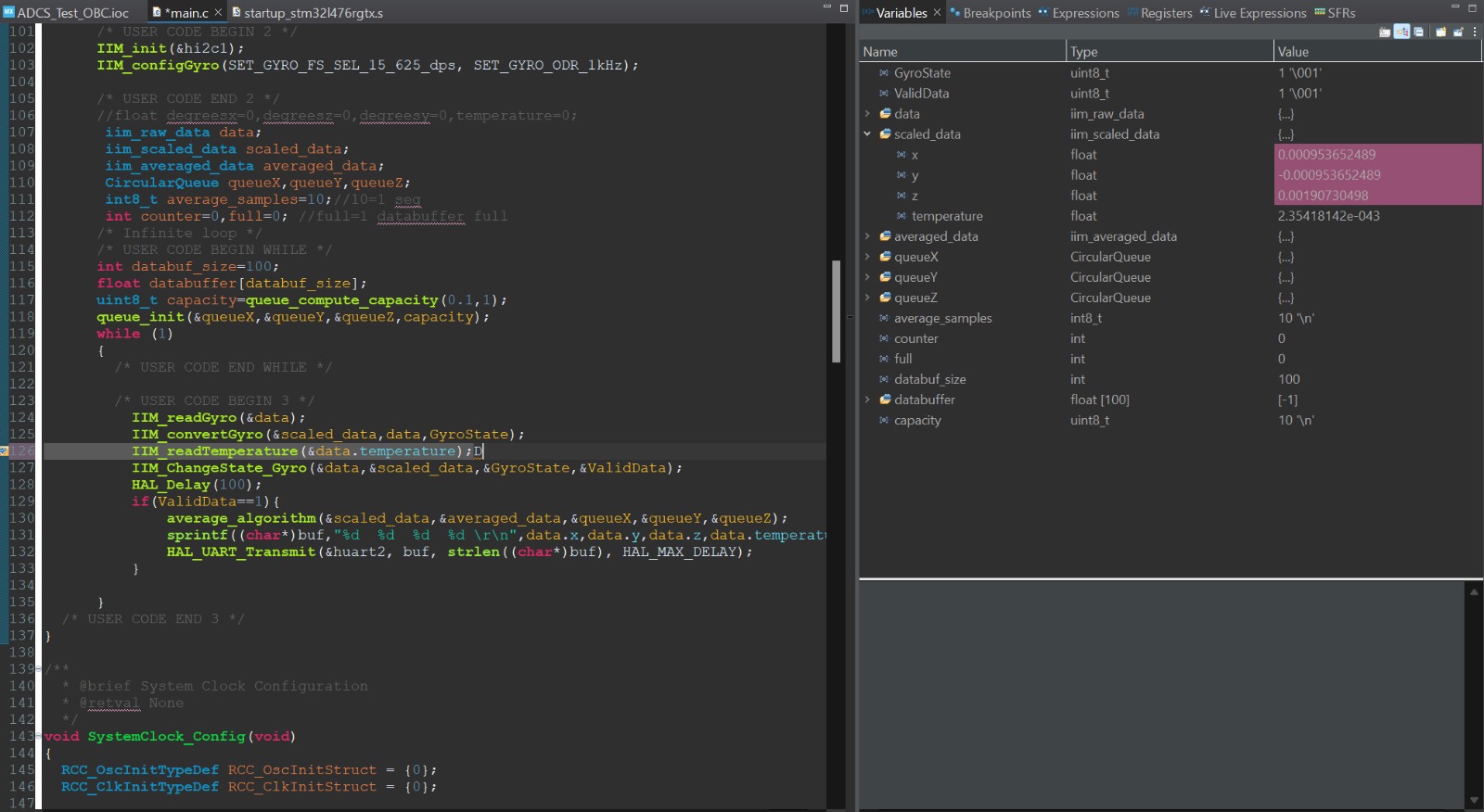
After including the "latboard_temp_sensor.h" in the "adcs.h" file which is included in the "main.h" file and calling the previously mentioned function in int main() of main.c, by stepping into it after debugging we can see:

At the end of the execution of the function, the previously talked about val_bfc and val_afc have the values 22 and 56.25 respectively, meaning a temperature of 22.56 °C.
Considering that everything else after the end of the execution of this functions runs as it should, meaning all tasks and all timers are created correctly, we can say that this test is also a success, meaning the absolute goal was accomplished.
Anomalies and mistakes
Making everything work for this test took considerably longer than expected, and here is a list of problems I faced that anyone who tries I2C communication should also consider and thoroughly verify:
1. Connection issues
Be it either cables being damaged, boards being improperly soldered, connectors not touching or any other one of these very common problems, I2C like any other communication protocol requires a strong and well defined signal, especially when trying to communicate something as delicate as an exact temperature value, where even a bit flip can have dramatic consequences.
The only real way to make sure that you're not experiencing any connection issues is to painstakingly check every possible connection by hand, firstly with a simple multimeter in order to make sure that your voltages are correct, and then with an oscilloscope in order to more finely analyze the signals transmitted.
Separating each connection and testing it individually is always better than trying to test everything when it's all connected, since there can be a lot of broken links in a bigger chain and it's way harder to identify which one is problematic.
2. Unfamiliar connectors
When working on any electronics project, you might very quickly come to see a component of any kind with which you are unfamiliar. In that case, instead of trying to work your way around a functionality of said component, it is always better to use it as it is intended, since that is the optimal way to make sure that you are not shooting yourself in the foot.
In our case, the lateral board has a 10/11 pin connector which requires special crimping of cables with a specialized Molex crimping tool in order for the connection to be strong. Trying without crimping has led quickly led me to the conclusion that, even though there might be a connection, for something like I2C a poor connection is as good as no connection.
3. Burned or damaged components
Every board that requires soldering is subject to damage: damage of the copper traces, damage of the lateral connectors, damage of the components, etc.
Sometimes it is better to make manually make sure that all your components are in working condition and that the connections between them are not damaged than just assume that's the case and have to suffer the potential consequences. Other times, changing them anyway might even be the safer strategy.
4. Mistakes in the basic setup of the experiment
Be it either a mistake in the physical setup, the setup in the IDE or even a big gap in the logic of the code itself, these mistakes are extremely common and do happen to everyone.
The only way to prevent this is to check even the things that you consider to be the most basic and logical things from the get go. Read all the documentation for the chips you are using, thoroughly consult all the schematics for the circuits that you are using and never assume that if something worked in a specific way with a board that it should work exactly the same with another one.
Conclusions
The I2C testing of the temperature sensor from the lateral boards was a complete success and now we can be sure that we have an OBC-COMMS board with working I2C pins that is ready for further testing of the peripherals.
TEST 6: ADCS gyroscope data read with OBC
Test Description and Objectives
The aim of this test is to verify that the OBC payload can establish a correct communication with the ADCS board and receive data from the gyroscope.
Requirements Verification
| Requirement ID | Description |
|---|---|
|
OBC-411 |
The ADCS board must be powered using the Nucleo board's output. |
|
OBC-412 |
Using the Nucleo, the I2C communication between the gyroscope and the MCU must be established, and the data must be correctly transmitted. |
|
OBC-421 |
The ADCS board must be powered using the ST-Link/V2 output. |
|
OBC-422 |
The ADCS board and the OBC board should be able to communicate data from the gyroscope to the MCU through I2C. |
|
OBC-431 |
The gyroscope reading function must be defined and integrated in the main code from GitHub. |
|
OBC-432 |
The complete GitHub code, including the newly written function, must be flashed onto the OBC-COMMS board using the ST-Link/V2 programmer. |
|
OBC-433 |
Using the already flashed OBC-COMMS board, it must be shown that the I2C communication between the chips still works when the previously integrated function is called in the main(). |
Test Setup
This is the list of required materials for this test:
- ADCS board
- OBC-COMMS board
- ST-Link/V2
- Power Supply
- Wires
- 2 x 4.7k Ω resistors (pull-up)
- Multimeter
- Oscilloscope
- Calculator, pen and paper
- Laptop with STM32CubeIde and Ki-Cad installed
Pass/Fail Criteria
The test will be verified if the requirements mentioned before are fulfilled. If in one of them it is detected any anomaly it will have to be corrected, otherwise the board can not pass to the other tests.
Test Plan
7.5.1. The Nucleo board test
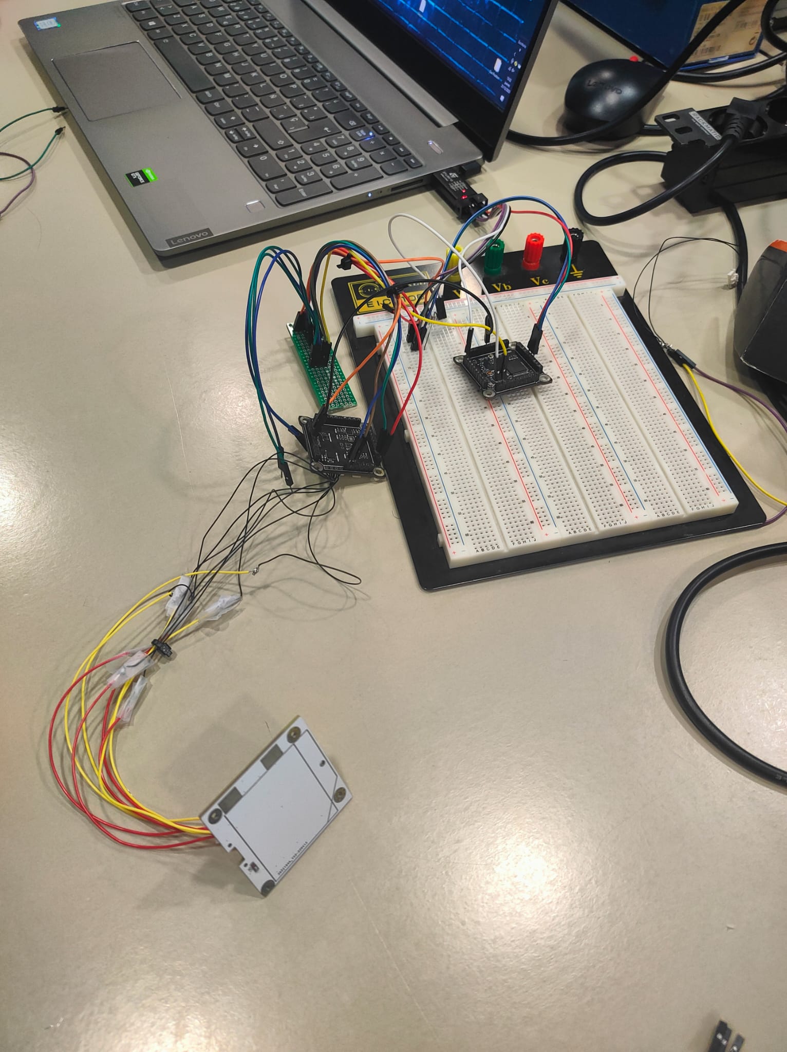
This is a picture of the setup for the Nucleo board test:

To complete this test, the following steps should be followed:
Step 1: Connect the 3.3V pin to the ADCS PCB.
Step 2: With the help of the multimeter, check that the VCC inputs pins has the correct value.
Step 3: Connect the Nucleo's SCL and SDA pins to the ADCS's corresponding I2C 3 pins.
Step 4: Prepare a code that can read from the gyroscope using I2C
Step 5: Run the code into the Nucleo and debug it step by step to see if the communication between the Nucleo and the ADCS has been done.
7.5.2. The OBC-COMMS board test
This is a picture of the setup:

These are the steps to follow:
Step 1: Connect the power supply from the ST-Link/V2 to the ADCS PCB and OBC PCB
Step 2: With the help of the multimeter, check that the VCC inputs pins has the correct value
Step 3: Connect the OBC payload to the computer using SWDIO pins
Step 4: Prepare a code that can read from the gyroscope using I2C
Step 5: Connect the OBC to the ADCS PCB using SCL and SDA pins
Step 6: Run the code into the OBC and look in the memory register to see if the communication between the OBC and the ADCS has been done.
Test Results
This is the code used for the Nucleo - ADCS data read test:
/* Includes ------------------------------------------------------------------*/
#include "main.h"
#include "iim42652.h"
#include "Sumador.h"
#include <string.h>
#include <stdio.h>
#include <stdlib.h>
/* Private includes ----------------------------------------------------------/
/ USER CODE BEGIN Includes /
int buf[100];
/ USER CODE END Includes */
/* Private typedef -----------------------------------------------------------/
/ USER CODE BEGIN PTD */
/* USER CODE END PTD */
/* Private define ------------------------------------------------------------/
/ USER CODE BEGIN PD */
/* USER CODE END PD */
/* Private macro -------------------------------------------------------------/
/ USER CODE BEGIN PM */
/* USER CODE END PM */
/* Private variables ---------------------------------------------------------*/
I2C_HandleTypeDef hi2c1;
UART_HandleTypeDef huart2;
/* USER CODE BEGIN PV */
/* USER CODE END PV */
/* Private function prototypes -----------------------------------------------/
void SystemClock_Config(void);
static void MX_GPIO_Init(void);
static void MX_USART2_UART_Init(void);
static void MX_I2C1_Init(void);
/ USER CODE BEGIN PFP */
/* USER CODE END PFP */
/* Private user code ---------------------------------------------------------/
/ USER CODE BEGIN 0 */
/* USER CODE END 0 */
/**
-
@brief The application entry point.
-
@retval int
/
int main(void)
{
/ USER CODE BEGIN 1 /
uint8_t GyroState=1;
uint8_t ValidData=1; // 1=true,0=false
/ USER CODE END 1 */
/* MCU Configuration--------------------------------------------------------*/
/* Reset of all peripherals, Initializes the Flash interface and the Systick. */
HAL_Init();
/* USER CODE BEGIN Init */
/* USER CODE END Init */
/* Configure the system clock */
SystemClock_Config();
/* USER CODE BEGIN SysInit */
/* USER CODE END SysInit */
/* Initialize all configured peripherals /
MX_GPIO_Init();
MX_USART2_UART_Init();
MX_I2C1_Init();
/ USER CODE BEGIN 2 */
IIM_init(&hi2c1);
IIM_configGyro(SET_GYRO_FS_SEL_15_625_dps, SET_GYRO_ODR_1kHz);
/* USER CODE END 2 /
//float degreesx=0,degreesz=0,degreesy=0,temperature=0;
iim_raw_data data;
iim_scaled_data scaled_data;
iim_averaged_data averaged_data;
CircularQueue queueX,queueY,queueZ;
int8_t average_samples=10;//10=1 seg
int counter=0,full=0; //full=1 databuffer full
/ Infinite loop /
/ USER CODE BEGIN WHILE /
int databuf_size=100;
float databuffer[databuf_size];
uint8_t capacity=queue_compute_capacity(0.1,1);
queue_init(&queueX,&queueY,&queueZ,capacity);
while (1)
{
/ USER CODE END WHILE */
/* USER CODE BEGIN 3 */
IIM_readGyro(&data);
IIM_convertGyro(&scaled_data,data,GyroState);
IIM_readTemperature(&data.temperature);D
IIM_ChangeState_Gyro(&data,&scaled_data,&GyroState,&ValidData);
HAL_Delay(100);
if(ValidData==1){
average_algorithm(&scaled_data,&averaged_data,&queueX,&queueY,&queueZ);
sprintf((char*)buf,"%d %d %d %d \r\n",data.x,data.y,data.z,data.temperature);
HAL_UART_Transmit(&huart2, buf, strlen((char*)buf), HAL_MAX_DELAY);
}
}
/* USER CODE END 3 */
}
INITIAL TESTING
Unfortunately, the ADCS board I worked with could not correctly flash this code, since there were issues with the 2 I2C pins who constantly remained at 0 V.
Even though I have briefly tried to figure out what the problem could be, it seems like there are more things wrong with that board.
That being said, Edgar Hernandez Recio, the ADCS responsible who wrote the code from above, did manage to flash and correctly transmit gyroscope data through I2C with this code, using another board.
So, this test is a success, but it will need replicating if I want to test the OBC-COMMS -> ADCS communication, most likely with the only ADCS board that seems to work.
FURTHER TESTING
After I changed the ADCS board from the one that obviously wasn't working to Edgar's working board and working together with him in order to make sure that we have the correct software configuration inside the IDE (correct code + correct pinout), we managed to replicate the Nucleo board test with my laptop, resulting in a complete success of test 1.
After that, I changed the configuration to the one for the OBC-COMMS test, again worked with Edgar to ensure that everything is as intended, and managed to communicate through I2C between the OBC-COMMS board and the ADCS board, resulting in a complete success of test 2 and, by proxy, the entire experiment.
This is how a correct non-moving test with correct values is supposed to look. All of the 3 values from the 3 axis of the gyroscope are pretty much 0, indicating complete stillness.
Anomalies
The biggest anomaly that we faced is that only one of the ADCS boards we have is fully operational.
This could be due to many factors, some of the most likely culprits being:
- bad soldering;
- burned components;
- bad connectors.
In order to increase the efficiency of the workflow, the recommendable thing to do is fix at least one of the non-working ADCS boards, as to enable multiple people testing with ADCS at the same time. The best solution to doing this is to completely resolder new components from scratch, since that is the only way to ensure that everything will be working as intended.
Conclusions
The ADCS gyroscope data read test was a complete success, so that means that we can continue with the peripheral testing and also have the certainty that at least one ADCS board is fully operational.
TEST 7: ADCS photodiode data read and ADC data converting with OBC
Test Description and Objectives
The aim of this test is to verify that the OBC which was previously shown to be able to establish a correct communication with the ADCS board can also correctly read data from the photodiode, meaning that both the photodiode itself and the Analog to Digital Converter must work as intended.
Requirements Verification
| Requirement ID | Description |
|---|---|
|
OBC-511 |
The ADCS board and lateral board must be powered using the Nucleo board's output. |
|
OBC-512 |
Using the Nucleo, the I2C communication between the photodiode and the MCU must be established and the data must be correctly transmitted once it has been converted by the ADC. |
|
OBC-521 |
The ADCS board and lateral board must be powered using the ST-Link/V2 output. |
|
OBC-522 |
The ADCS board, the OBC board and the lateral board should be able to communicate data from the photodiode through I2C and the readable data correctly converted by the ADC. |
|
OBC-531 |
The photodiode reading function must be defined and integrated in the main code from GitHub. |
|
OBC-532 |
The complete GitHub code, including the newly written function, must be flashed onto the OBC-COMMS board using the ST-Link/V2 programmer. |
|
OBC-533 |
Using the already flashed OBC-COMMS board, it must be shown that the I2C communication between the chips still works when the previously integrated function is called in the main(). |
Test Setup
This is the list of required materials for this test:
- ADCS board
- OBC-COMMS board
- Lateral board with a photodiode
- ST-Link/V2
- Powerful halogen lamp
- Power Supply
- Wires
- 2 x 4.7k Ω resistors (pull-up)
- Multimeter
- Oscilloscope
- Calculator, pen and paper
- Laptop with STM32CubeIde and Ki-Cad installed
Pass/Fail Criteria
The test will be verified if the requirements mentioned before are fulfilled. If in one of them it is detected any anomaly it will have to be corrected, otherwise the board can not pass to the other tests.
Test Plan
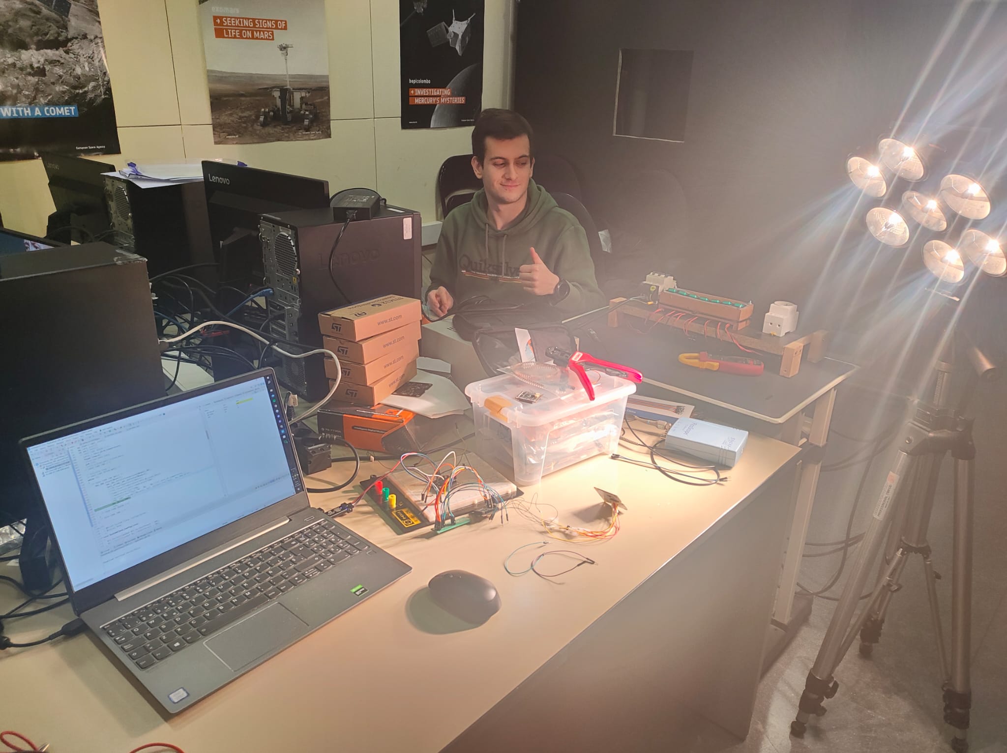
This is the picture of the necessary setup (and a cameo by Artur):
These are the steps to follow:
Step 1: Connect the power supply from the ST-Link/V2 to the ADCS PCB, OBC PCB and lateral board.
Step 2: With the help of the multimeter, check that the VCC inputs pins has the correct value
Step 3: Connect the OBC payload to the computer using SWDIO pins
Step 4: Prepare a code that can read from the photodiode using I2C
Step 5: Connect the OBC to the ADCS PCB using SCL, SDA and ADC-PH pins
Step 6: Connect the lateral board with the ADC-PH pin to the same pins from the 2 PCBs
Step 7: Run the code into the OBC and look in the memory register to see if the communication between the OBC and the ADCS has been done.
Test Results
This is the code used for the OBC-ADCS photodiode and ADC test:
#include "main.h"
/* Private includes ----------------------------------------------------------/
/ USER CODE BEGIN Includes /
int buf[100];
/ USER CODE END Includes */
/* Private typedef -----------------------------------------------------------/
/ USER CODE BEGIN PTD */
/* USER CODE END PTD */
/* Private define ------------------------------------------------------------/
/ USER CODE BEGIN PD */
/* USER CODE END PD */
/* Private macro -------------------------------------------------------------/
/ USER CODE BEGIN PM */
/* USER CODE END PM */
/* Private variables ---------------------------------------------------------*/
ADC_HandleTypeDef hadc1;
I2C_HandleTypeDef hi2c1;
UART_HandleTypeDef huart2;
/* USER CODE BEGIN PV */
/* USER CODE END PV */
/* Private function prototypes -----------------------------------------------/
void SystemClock_Config(void);
static void MX_GPIO_Init(void);
static void MX_USART2_UART_Init(void);
static void MX_I2C1_Init(void);
static void MX_ADC1_Init(void);
/ USER CODE BEGIN PFP */
/* USER CODE END PFP */
/* Private user code ---------------------------------------------------------/
/ USER CODE BEGIN 0 */
/* USER CODE END 0 */
/**
- @brief The application entry point.
- @retval int
/
int main(void)
{
/ USER CODE BEGIN 1 */
/* USER CODE END 1 */
/* MCU Configuration--------------------------------------------------------*/
/* Reset of all peripherals, Initializes the Flash interface and the Systick. */
HAL_Init();
/* USER CODE BEGIN Init */
/* USER CODE END Init */
/* Configure the system clock */
SystemClock_Config();
/* USER CODE BEGIN SysInit */
/* USER CODE END SysInit */
/* Initialize all configured peripherals /
MX_GPIO_Init();
MX_USART2_UART_Init();
MX_I2C1_Init();
MX_ADC1_Init();
/ USER CODE BEGIN 2 /
int16_t data_ph=0,temperature;
float temp=0;
//tcn_raw_data data;
int i=1;
//tcn_scaled_data scaled_data;
/ USER CODE END 2 */
/* Infinite loop /
/ USER CODE BEGIN WHILE /
while (1)
{
/ USER CODE END WHILE /
HAL_ADC_Start(&hadc1);
HAL_ADC_PollForConversion(&hadc1,20);
data_ph=HAL_ADC_GetValue(&hadc1);
//TCN_readTemperature(&data);
//TCN_convertTemperature(data,&scaled_data);
//temp=(scaled_data.temperature100);
//temperature=(int)temp;
//sprintf((char*)buf,"%d %d %d \r\n",data_ph,temperature,i);
//HAL_UART_Transmit(&huart2, buf, strlen((char*)buf), HAL_MAX_DELAY);
HAL_Delay(100);
i++;
/* USER CODE BEGIN 3 /
}
/ USER CODE END 3 */
}
TEST RESULTS
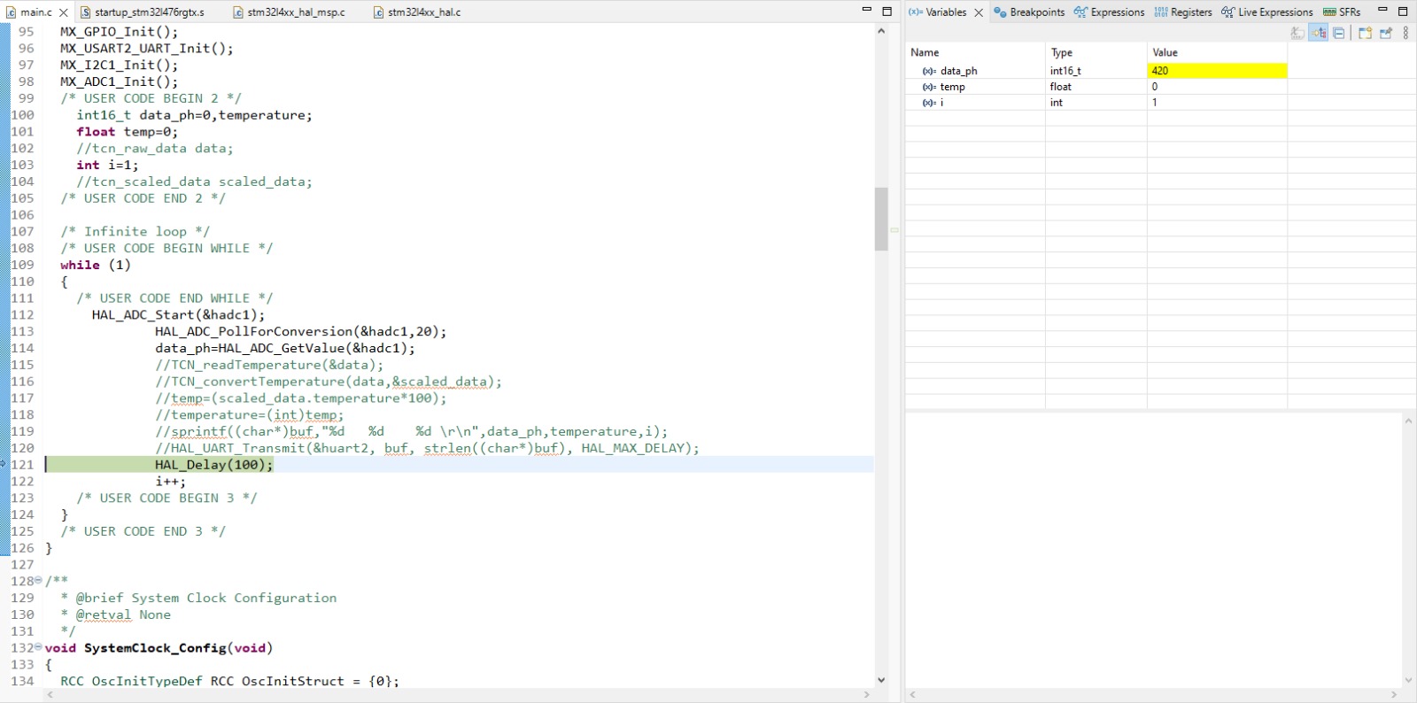
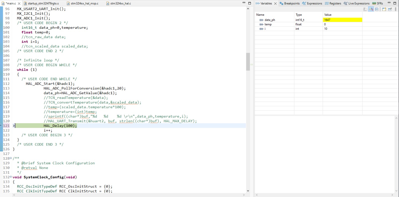
After a few usual connection issues, the test went smoothly from what was basically the first attempt. Having a halogen lamp with multiple modules, we could test the reading with a lot of different settings, and we found that the number of modules that are lit is almost proportional to the value we read, meaning the test was in fact a success. Below are the results for 3 different light readings: no lights, 2 lights and 7 lights. The relevant variable is "data_ph", marked in yellow since it has just changed value.

Anomalies
In this test, apart from the usual connection issues, we encountered no notable anomalies.
Conclusions
The ADCS-OBC photodiode data read and ADC data converting test was a complete success, meaning we have managed to test another one of the functionalities of the system and that we are getting closer to a fully integrated system test.
No Comments