Subsystem Verification (SSV)
The purpose of this section is to conduct a complete test of the COMMS subsystem following the soldering of the board or after completing environmental tests. These tests are essential to ensure that the COMMS subsystem hardware is functioning as intended.
The entire test is outlined in the following diagram:
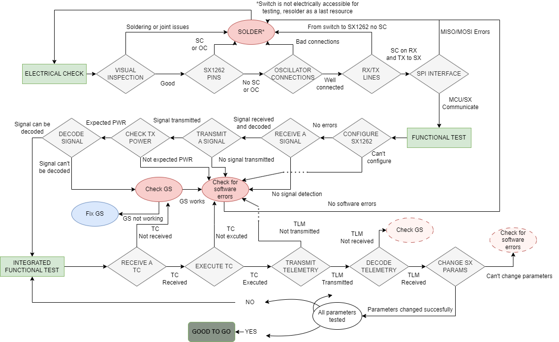
Figure 1: COMMS Development and Verification Plan.
COMMS SDV starts with a visual inspection of the soldered board, in search for easily detectable mistakes and solder issues. The next step is to manually verify the connections on the SX1262 (Transciever) pins, as OC might be common if care is not taken when soldering. The oscillator presents as a moderately hard to solder piece so it is easy and useful to ensure that the lines connecting the crystal to the SX1262 and the planes are properly set-up. A critical piece to verify is the switch, but to do so electrical checks are not easy to perform. Its status will be verified by the transmission and reception operations. RX/TX go all the way from the switch to the transciever, so a simple contituity check suffices to verify the line integrity, Finnally, with the help of the OBC the SPI interface is tested to verify communications.
As communication between the MCU and the SX is ensured it is time to test the basic operations to be performed by the COMMS subsystem, mainly receival and decoding as well as transmission of signals at appropiate power. Several points of failure appear in these steps, mainly software errors and GS errors. It might also occur that the previous electrical check did not completely sort out all isues, creating the need for further hardware inspection.
The final steps are to verify the board and susbsystem is to test several operations to be done by it. Telecommands are to be received, executed and telemetry is to be transmitted and decoded by the GS. Finally it is optimal to test the system with different configurations as parameters might be changed on-the-fly during the mission. If this step is accomplished the board is considered good to go.
Electrical Check
Test Description and Objectives
The purpose of this section is to conduct an electrical check of the COMMS subsystem following the soldering of the board or after completing environmental tests.
Always ensure you're grounded to prevent static electricity from damaging the electronic components on the board.
Requirements Verification
| Requirement ID | Description |
|---|---|
| COMMS-EC-001 | All components and connections shall be visually inspected to ensure proper soldering, absence of damage, and correct placement of wires. |
| COMMS-EC-002 | Each SX1262 pin shall be securely connected to its corresponding circuit point, with no shorts or floating pins present. |
| COMMS-EC-003 | The oscillator shall be checked to ensure its connections are properly soldered and it is operating at the specified frequency. |
| COMMS-EC-004 | The receive (RX) and transmit (TX) lines shall be inspected to confirm they are properly wired, with no interference or signal degradation. |
| COMMS-EC-005 | The SPI interface shall be validated to ensure correct wiring and successful communication between the microcontroller and the SX1262. |
| COMMS-EC-006 | All solder joints shall be inspected to verify they are strong and free from defects, with any weak joints re-soldered as needed. |
Test Set-Up
- OBC-COMMS board.
- Multimeter
- Microscope
- Soldering station
Pass/Fail Criteria
| Description | Pass Criteria | Fail Criteria |
|---|---|---|
| Visual inspection of components, soldering, and wire placement. | Components and lines are securely soldered and correctly positioned, with no visible cracks in the soldering or components, melted parts, or misaligned elements. | Improper soldering, damage, or incorrect placement. |
| Secure connections for SX1262 pins, with no shorts or floating pins. | All pins are securely connected, no shorts or floating pins. | Pins are loose, shorted, or floating. |
| Check oscillator connections and frequency. | Oscillator is correctly soldered and operates at the right frequency. | Faulty connections or incorrect frequency. |
| Inspect RX and TX lines for proper line and signal quality. | RX and TX lines are correctly connected with no signal issues. | No signal, interference, or signal degradation are observed. |
| Validate SPI interfaces and communication. | SPI is correctly connected and communication is successful. | Incorrect connection or communication failure. |
| Inspect solder joints for strength and defects. | Solder joints are strong and defect-free. | Weak or defective joints require re-soldering. |
Test Plan
| Step - ID | Description |
| EC-TEST-01 | Using a microscope or equivalent tool, perform a visual inspection of the OBC-COMMS board to check for damaged components or traces, as well as displaced or missing components, and cracks in the solder joints. If any damaged elements are identified, replace them or conduct additional tests to assess their functionality. |
| EC-TEST-02 | Using a multimeter, verify that all pins of the transceiver (SX1262) are properly soldered, correctly positioned, and free of any unwanted short circuits or open circuits. |
| EC-TEST-03 | Repeat the previous step for the oscillator connections. |
| EC-TEST-04 | Use a multimeter to verify that the entire RX-TX chain is free of any unwanted shorts or open circuits. Pay extra attention to the switch, as it has 6 pins in a confined space. |
| EC-TEST-05 | After inspecting the COMMS subsystem, the final step is to verify the connections between the transceiver and the On-Board Computer. Specifically, use a multimeter to ensure that all SPI connections are secure. The pins to check include SX1262_NSS, SCK, MOSI, MISO, SX1262_NRST, and SX1262_BUSY. |
If the electrical check is successful, proceed to the functional testing of the COMMS subsystem. Keep in mind that in some cases, such as after a vibration test, the board may sustain subtle damage, so proceed with extra caution!
Functional test
Test Description and Objectives
The purpose of the functional test is to achieve a successful transmission using the OBC-COMMS board.
Requirements Verification
| Requirement ID | Description |
|---|---|
| COMMS-FT-001 | The SX1262 configuration parameters (SF=11, CR=4/5), including frequency (868 MHz), modulation (LoRa), and power settings, shall be correctly set for the test. |
| COMMS-FT-002 | The device shall transmit a signal that is detectable at the intended range (frequency and power) with minimal signal degradation. |
| COMMS-FT-003 | The transmission power level shall be verified to meet specified limits and be consistent with expected output. |
| COMMS-FT-004 | The device shall successfully receive signals without interference or loss of quality during the test. |
| COMMS-FT-005 | The device shall decode incoming signals accurately without errors during the functional test. |
Test Set-Up
- OBC-COMMS board.
- Spectrum Analyzer
- ST-LINK v2
- Laptop
Pass/Fail Criteria
| Description | Pass Criteria | Fail Criteria |
|---|---|---|
| The SX1262 configuration parameters (SF=11, CR=4/5), including frequency (868 MHz), modulation (LoRa), and power settings, shall be correctly set for the test. | Parameters are set correctly as per specification (SF=11, CR=4/5, frequency=868 MHz, modulation=LoRa, power at specified level). | Parameters are incorrectly set, or any configuration setting is missing or erroneous. |
| The device shall transmit a signal that is detectable at the intended range (frequency and power) with minimal signal degradation. | Signal is transmitted and detected within the specified range, with acceptable signal quality and minimal degradation. | Signal is not detectable, outside the intended range, or shows significant degradation. |
| The transmission power level shall be verified to meet specified limits and be consistent with expected output. | Transmission power meets specified limits and aligns with expected power output. | Transmission power is inconsistent with expected output. |
| The device shall successfully receive signals without interference or loss of quality during the test. | Signals are received with clarity, no interference, and within acceptable quality limits. | Signal reception is poor, shows interference, or lacks quality. |
| The device shall decode incoming signals accurately without errors during the functional test. | Signals are decoded correctly without errors, and data integrity is maintained. | Decoding fails, produces errors, or results in data integrity loss. |
Test Plan
| Step - ID | Description |
| FT-TEST-01 | Connect the OBC-COMMS board to a computer using the ST-LINK v2, concretely connect the RST, 3.3V, GND, SWCLK and SWDIO pins to the board. |
| FT-TEST-02 | After connecting the board to the laptop using an ST-LINK, upload the code to the board. You may want to add breakpoints to examine each step of the transmission process in detail. |
| FT-TEST-03 | After flashing the code, use a Spectrum Analyzer to visualize the transmission’s power, frequency, and other parameters more effectively. |
| FT-TEST-04 | After verifying the basic parameters of the transmitted signal, proceed to test the Ground Station's ability to correctly decode the signal. Configure the a TinyGS for a reception test of the transmitted signal. |
| FT-TEST-05 | Transmit a signal, ideally containing user-generated telemetry data, and verify that the Ground Station has accurately received and decoded all transmitted information. This test can be repeated with different types of data, such as payload data. |
Integrated functional test
Test Description and Objectives
Requirements Verification
| Requirement ID | Description |
|---|---|
| COMMS-IFT-001 | The system can receive telecommands, including those consisting of multiple packets. |
| COMMS-IFT-002 | The COMMS system successfully executes telecommands upon correct reception and generates a response if the telecommand requires it. |
| COMMS-IFT-003 | Once a response is generated, the COMMS subsystem transmits it accurately at the specified frequency (868 MHz), output power (22 dBm), spreading factor (11), and coding rate (4/5). Same requirement applies for the telemetry which is sent periodically by the spacecraft. |
| COMMS-IFT-004 | The received telemetry and/or telecommand is correctly decoded by the Ground Station. |
| COMMS-IFT-005 | All parameters updated via telecommand on the PocketQube are accurately applied, including configuration adjustments and payload activation settings. |
Test Set-Up
Pass/Fail Criteria
| Description | Pass Criteria | Fail Criteria |
|---|---|---|
| x | x | x |
| x | x | x |
| x | x | x |
| x | x | x |
Test Plan
| Step - ID | Description |
| x | x |
| x | x |
| x | x |
| x | x |
| x | x |
No Comments