Structure
Document scope
This document aims to provide both an in-depth description of structural elements and general architecture, as well as a basis for understanding the way all the subsystems and devices are connected throughout the PocketQube.
In addition in the following link you can find the PCB design repository: https://github.com/nanosatlab/pocat-hw
General structure
This project follows the PocketQube mechanical standard. It doesn’t however specify the way that the inner part of the spacecraft needs to be organised. As a result, considering the very little space available and the complexity of the avionics, the proposed solution for the inner structure will be presented below.
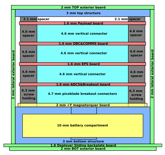
In this representation, we can distinguish different parts that make up the structure. In green, we can see the outer boards, which form the external part of the satellite. On the bottom exterior board, we will find the killswitches, while the deployer sliding backplate will be the only PCB in contact with the deployer rail. Regarding the top exterior board, this part will be replaced by the payload used for each satellite. If the payload can be implemented on a single PCB (Payload board), this top exterior board could remain in place. In the case of our payloads, both the K-Band and the L-Band, the top exterior board will be replaced by the payload board.
In blue, we can see the only two internal structures that are not PCBs. The bottom structure will house the battery and act as an interface between the bottom exterior board and the sliding plate, connecting them with the rest of the subsystem stack. This structure will be made of PTFE (Teflon). The top structure, made of 7075 Aluminium Alloy, will be used for the K-Band, acting as the interface between the payload and the rest of the subsystem stack. Additionally, both structures will allow the lateral boards to be screwed into them.
In red, we find the PCBs that form the various subsystems. From top to bottom, these are: the Payload board (for the payload, additional PCBs may be added inside the payload), the OBC and COMMS board, the EPS board, and the ADCS board. These PCBs will be connected to each other via the vertical connectors, shown in cyan, which allow electrical interconnection between all the PCBs in the stack.
In gray, the spacers distribute the force from the tightened screws, preventing the vertical pins from bearing the full load.
Finally, in yellow, we see the +Y magnetorquer and the battery. The +Y magnetorquer will be attached and screwed into the bottom structure.
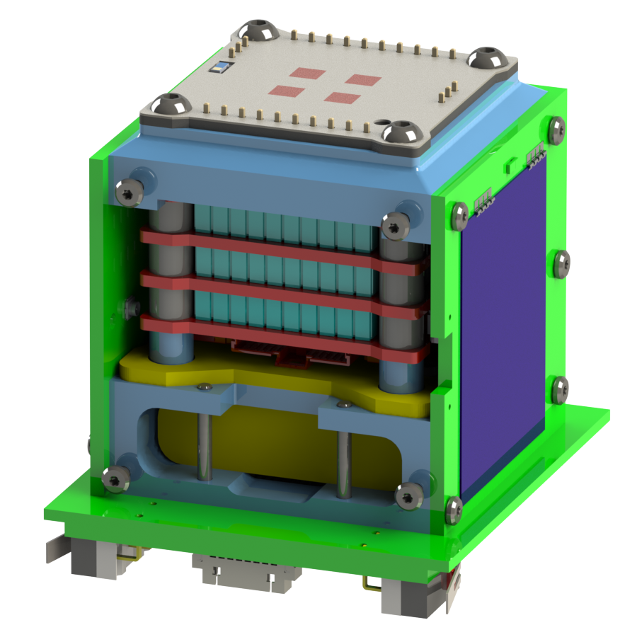
The core of the satelite comprises a set of PCBs containing the main circuitry. These are supported by Polytetrafluoroethylene (PTFE), commonly known as Teflon, which encases and protects the internal battery. Additionally, there are screw holes to secure the internal stack and mounts for the lower PCB and side boards. The other structure, made of 7075 aluminum, supports the K-Band payload and is located at the top of the PCB stack. It also includes screw holes to secure the internal stack and payload, as well as mounts for the upper PCB and side boards.
The 3D CAD model of the satellite is located in the attached documents folder in .STEP format Regarding the screws and spacers, all are stainless steel (INOX). The upper screws that go through the entire satellite along the Y axis are ISO7380 M3x35mm. The other screws are ISO14580, varying in length but all M2. Concerning the spacers, these are M3, with a main length of 4mm, and additional ones that can be added as needed up to 4.6mm.
To secure screws onto structures, Helicoils are used, allowing stainless steel screws to be screwed into materials like PTFE or aluminum without causing damage. This is because stainless steel is much harder than PTFE or aluminum and could potentially damage them if screwed directly. Therefore, the Helicoil acts as an intermediary between the screw and the material, ensuring a secure fixation without damage.
Structural materials
At this stage, the materials intended for the satellite structure will be specified. In the attached DML file, more detailed information is provided regarding the properties, location, and outgassing parameters of these materials. Here, we will offer a more general overview of the materials to be used.
- 7075 Aluminum Alloy: This material is used for the top structure of the satellite, which supports the K-Band payload. It is a high-strength material with excellent mechanical properties, making it ideal for this application. It is also lightweight, which is crucial for a satellite and prevent intermodulation interference between the Top and Bottom boards.
- Polytetrafluoroethylene (PTFE): This material is used for the bottom structure of the satellite, which houses the battery and serves as an interface between the lower exterior board and the sliding plate. It has low friction and high chemical resistance, making it a suitable choice for this function.
- Stainless Steel (INOX): This material is used for screws and spacers that secure components together, such as the side panels and bottom PCBs. It is a durable, corrosion-resistant material, making it ideal for this purpose.
- FR-4: This material is used for the PCBs that form the various subsystems of the satellite. Once the PCBs are soldered and tested, a conformal coating will be applied to protect them from moisture and other external factors.
- RT/DUROID 5880: This material is used for the K-Band antenna, as it has excellent dielectric properties and is suitable for high-frequency applications.
Interfaces
The satelite according to the 1P standard, consist of a 50 x 50 x 50 mm3 cube, placed onto a 64 x 58 mm2 interface board, the latter acting as the mechanical interface between the satellite and the deployer pod. The contact is done by having the PCB edges represented in grey in the figure below slide into the deployer rails, with the cube being fixed and later launched along the +Z direction. Lastly, this interface board serves only the purpose described above, and in the -Y direction, another PCB is mounted in order to house the circuitry correspondent to the ventral side of the cube.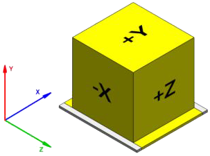
The interface between subsystems is established through vertical pins, allowing electrical connections between the different stacked PCBs. A distinction must be made between the Payload pins and those of the subsystems.
- Subsystem stack: The vertical connections between different PCBs will be established using vertical connectors, allowing the pins to pass through all the PCBs until they reach the required one. Each subsystem features 4 vertical connectors, each with 10 pins, providing a total of 40 pins for distributing various signals, sensors, and others components.
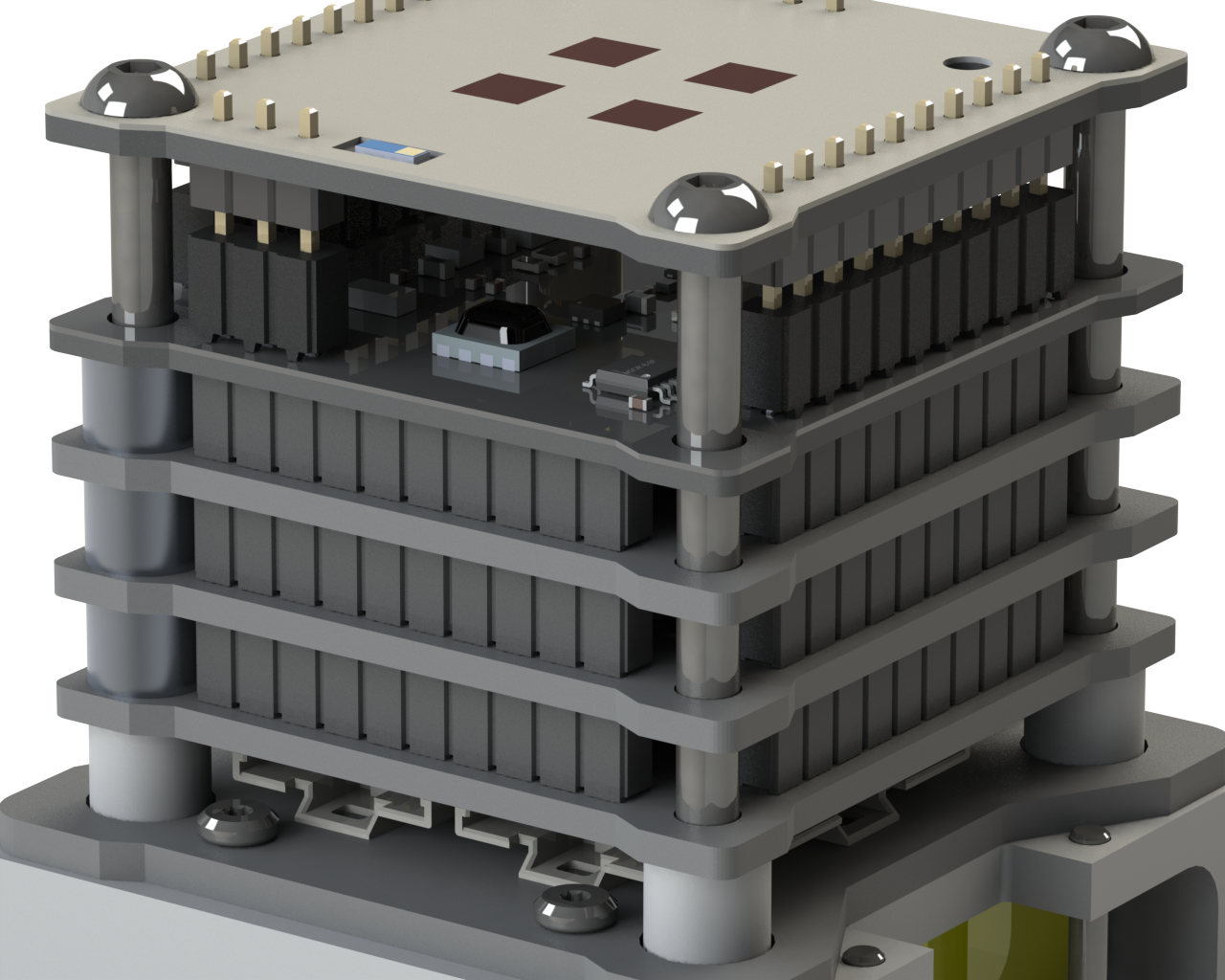
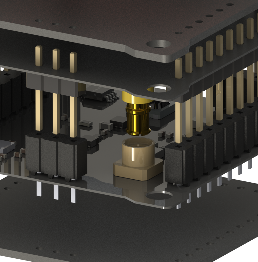
- Payload: there are three different types of vertical connectors. The PCB connecting the payload to the OBCCOMMS uses the same connector as the rest of the subsystem stack, while different connectors are used on the RF Front-End Top PCB. Another vertical connector, an SMP connector, is used in the payload to carry the RF signal from one level to another. In figure below the three types of connectors can be observed.
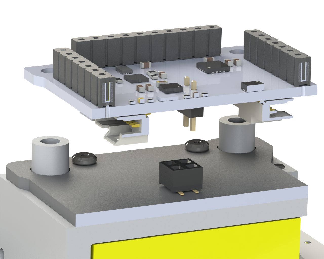
- Mag +Y: It is also important to highlight the connection between the magnetorquer and the ADCS, as this is also done with vertical pins. If we section the satellite in half, these pins would look as below:
Mass budget and moments of inertia
| Component | Manufacturer / Supplier | Mass (g) | Source |
| Screws | |||
| M2x6 Torx ISO14580 | FIXNVIS | 0,2 | Measured |
| M2x20 Torx ISO14580 | FIXNVIS | 0,5 | Measured |
| M2x5 Torx ISO14580 | FIXNVIS | 0,2 | Measured |
| M3x35 Hex ISO7380 | FIXNVIS | 1,7 | Measured |
| Spacers | |||
| M3x4 Spacer | RAF Electronic Hardware / MOUSER | 0,2 | Datasheet |
| M3x0.5 Spacer | TORRAS | 0,1 | Measured |
| M2x5 Spacer | Bivar / MOUSER | <0.1 | Datasheet |
| Power Energy | |||
| Solar Cell | Lightricity | 1,4 | Datasheet |
| LiPo Battery | DNK | 34 | Measured |
| Subsystem and outer PCBs | |||
| Bottom PCB with components | In-house | 16,6 | Measured |
| Sliding Plate | In-house | 8,4 | Measured |
| Lateral PCB with component | In-house | 11,1 | Measured |
| Y+ Mag PCB with components | In-house | 6,6 | Measured |
| AOCS PCB with components | In-house | 10,2 | Measured |
| EPS PCB with components | In-house | 9,3 | Measured |
| OCB-COMMS PCB with components | In-house | 9,2 | Measured |
| Structure | |||
| Bottom structure | PCBWay | 30 | Measured |
| Payload: K-band | |||
| K-band antenna | PCBWay | 0,7 | Measured |
| Support FR-4 PCB | PCBWay | 7,6 | Measured |
| RF top PCB with components | PCBWay | ||
| Top structure | PCBWay | 24,3 | Measured |
| RF bottom PCB with components | PCBWay | 9,2 | Measured |
| Interface PCB with components | PCBWay | ||
| Flat Wires | |||
| 3 pin PicoBlade - PicoClasp | Molex / MOUSER | 0,3 | Measured |
| 10 pin PicoBlade - PicoClasp | Molex / MOUSER | 1,2 | Measured |
| 15 pin PicoBlade - PicoClasp | Molex / MOUSER | 1,8 | Measured |
- The total weight of the Payload KBand is 41.8 g.
- The combined weight of the subsystems PCBs (no PL) is 28.7 g.
- The outer boards with solar cells, the total weight amounts to 76.4 g.
- The weight of all screws used in the satellite is 12.52 g.
- The total weight of spacers used in the satellite is 3.6 g.
- The Bottom structure, including the internal battery, weighs 64.0 g.
- The total weight of the flat wires is 6.9 g.
The total weight of the satellite is 234 g. A mass below 250 g, thus meeting the mass requirement specified in the PocketQube standard.
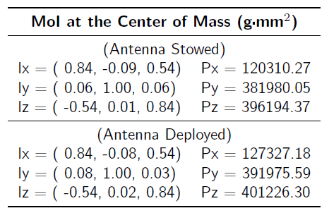
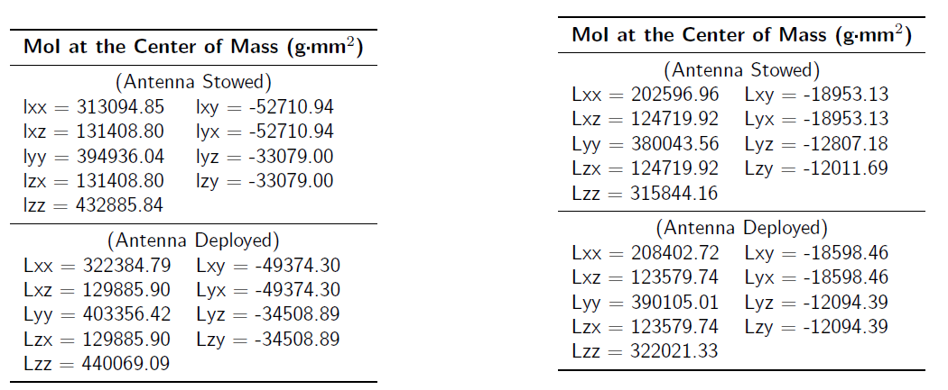
Considering possible variations such as varying solder amounts on PCBs, cable lengths for flat wires and the Helicoils (though their weight is negligible), a tolerance of ±15 g is added to the final weight of the satellite. Regarding the Center of Mass (CoM) in relation to spacecraft geometry , Moments of Inertia (MoI) relative to the CoM , and with respect to both the CoM and spacecraft coordinate frame, the following results have been obtained:

Pin description from the OBC perspective
| Pin Name | Connector | Pin Number | Type | Description |
| SDA1 | J1 | 1 | I2C | I2C1 data bus |
| SCL1 | J1 | 2 | I2C | I2C1 clock bus |
| UART_RX | J1 | 3 | UART | UART RX bus |
| KILLSWITCH+ | J1 | 4 | Digital | Killswitch positive terminal. |
| PFO | J1 | 5 | Digital Input | Battery fail status pin |
| BATT- | J1 | 6 | Power | Negative terminal of the battery |
| NC | J1 | 7 | Not connected | Free pin for testing & debugging. |
| UART_TX | J1 | 8 | UART | UART TX bus |
| GND | J1 | 9 | Power | Ground pin |
| VCC | J1 | 10 | Power | General Power line: 3.3V |
| STM32_PA15 | J2 | 1 | GPIO | Pin connected to STM32 PA15 pin, user defined |
| SWO | J2 | 2 | Serial-Wire Data P | STM32 debug pin |
| BATT_NTC | J2 | 3 | Analog | Battery temperature NTC sensor |
| SOLAR_Y | J2 | 4 | Power | Solar panel output voltage, Y axis |
| SEL_PH2 | J2 | 5 | Digital Output | Selector for the photodiode multiplexer |
| SEL_PH1 | J2 | 6 | Digital Output | Selector for the photodiode multiplexer |
| GND | J2 | 7 | Power | Ground pin |
| HEATER_PWR | J2 | 8 | Power | Power line that goes to the heater |
| BURNCOMMS | J2 | 9 | Digital Output | COMMS antenna thermal knife enable |
| GND | J2 | 10 | Power | Ground pin |
| SOLAR_Z | J3 | 1 | Power | Solar panel output voltage, Z axis |
| STM32_PB0 | J3 | 2 | GPIO | Pin connected to STM32 PB0 pin, user defined |
| ADCS_POWER | J3 | 3 | Power | ADCS Power line: 3.3V |
| RST_DRIVERS | J3 | 4 | Digital Input | Active low ADCS current driver reset |
| ADC_PH | J3 | 5 | Analog Input | Photodiode array output |
| P/L_POWER | J3 | 6 | Power | Payload Power line: 3.3V |
| SEL_PH0 | J3 | 7 | Digital Output | Selector for the photodiode multiplexer |
| VCC_UMBILICAL | J3 | 8 | Power | Umbilical power line |
| FAULT | J3 | 9 | Digital Input | Battery charging fault status pin |
| CHRG | J3 | 10 | Digital Input | Battery charging monitoring pin |
| SOLAR_X | J4 | 1 | Power | Solar panel output voltage, X axis |
| CHRGOFF | J4 | 2 | Digital Output | Battery charging enable pin |
| CLPROG | J4 | 3 | Analog Input | MPPT output current monitoring pin |
| SDA3 | J4 | 4 | I2C | I2C3 data bus |
| NRST | J4 | 5 | NRST | STM32 NRST signal |
| SWDIO | J4 | 6 | Serial-Wire Data I/O | STM32 debug port |
| SWCLK | J4 | 7 | Serial-Wire Clock | STM32 debug port |
| DAC_PL | J4 | 8 | Analog Output | STM32 DAC output for payload |
| ADC_PL | J4 | 9 | Analog Input | STM32 ADC input for payload |
| SCL3 | J4 | 10 | I2C | I2C3 clock bus |
I2C map
| Device | Bus | Address | Board | Description |
| TMP112 | I2C1-3.3 V | 1001000 | P/L3 frontend top | Temperature sensor for payload 3 |
| TCN75-P/L2 | I2C1-3.3V | 1001000 | P/L2 frontend bot | Temperature sensor for payload 2 |
| TCN75-Lat +X | I2C3-3.3 V | 1001001 | Lateral +X | Temperature sensor for PQ +X face |
| TCN75-Lat +Z | I2C3-3.3 V | 1001010 | Lateral +Z | Temperature sensor for PQ +Z face |
| TCN75-Lat -X | I2C3-3.3 V | 1001011 | Lateral -X | Temperature sensor for PQ -X face |
| TCN75-Lat -Z | I2C3-3.3 V | 1001100 | Lateral -Z | Temperature sensor for PQ +Z face |
| TCN75-Top +Y | I2C3-3.3 V | 1001101 | Top +Y | Temperature sensor for PQ +Y face |
| TCN75-Bot -Y | I2C3-3.3 V | 1001110 | Bottom -Y | Temperature sensor for PQ -Y face |
| TCN75-ADCS | I2C3-3.3 V | 1001111 | ADCS | Temperature sensor for the magnetorquer drivers |
| BD2606MVV | I2C3-3.3 V | 1100110 | ADCS | Magnetorquer driver |
| MMC5983MA | I2C3-3.3V | 0110000 | ADCS | Magnetometer |
| IIM-42652 | I2C3-3.3 V | 1101000 | ADCS | Inertial Momentum Unit |
| DS2782 | I2C3-3.3 V | 0110100 | EPS | Battery sensor |

No Comments