Antenna Design
INTRODUCTION
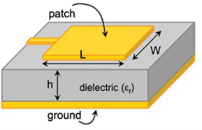
The goal of PoCat payload 3 is to identify Radio Frequency Interference (RFI) in the lower Ka-band (24-25 GHz). A patch antenna is chosen as the resonant element for its lightweight, 2D design, and reduced size due to the inverse frequency-wavelength relationship. A basic Microstrip Patch antenna consists of a conductive patch on one side of a dielectric substrate, with a ground plane on the other, emitting radiation through fringing fields at the patch edge.
Requirements and specifications

The design process is split in two main tasks. First, the single element design, includes choosing the appropriate substrate material, determine the patch antenna dimensions and the feedline that will match the patch with the rest of the array, and secondly, the design of the feeding network and the patches’ distribution.
SINGLE ELEMENT: MICROSTRIP PATCH ANTENNA
SUBSTRATE
To optimize antenna performance, the choice of substrate is crucial. A low dielectric constant (𝜀r) is preferred for minimal losses, improved efficiency, broader bandwidth, and better radiation. Increasing substrate height or reducing permittivity can also increase the bandwidth, but it may introduce undesired radiation and coupling to other components due to surface waves in the substrate. The loss tangent (tan(𝛿) or Df) is another main parameter affecting losses, with higher values indicating more dielectric absorption and losses. Rogers-5880, with a Df value of 0.0009 at 10GHz, is a suitable choice due to its low loss characteristics.
SINGLE ELEMENT DIMENSIONS
The initial patch dimensions are given by the following equation, which gives a patch side of ~4 mm using the Rogers-5880 substrate at a 24.5 GHz frequency.
The length of the patches may be changed to shift the resonances of the centre fundamental frequency of the individual patch elements. The resonant input resistance of a single patch can be decreased by increasing the width of the patch. This is acceptable if the relation between the patch width and patch length (W/L) does not exceed 2 since the aperture efficiency of a single patch begins to drop, as W/L increases beyond this value.
Patch antenna main parameters:
PATCH ANTENNA MATCHING
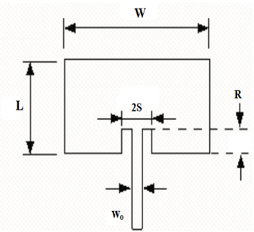
In this project, the chosen method is to use a microstrip line attached at the edge of the patch, combined with adding an inset into the patch itself as shown in the following figure.
The longitude of the inset R can be calculated with the following equation where Zin(R) is the matching impedance and Zin(0) is the impedance at the edge of the patch (if the patch was fed in the end).
Hence, by feeding the patch antenna as shown, the input impedance can be decreased to tune it at the desired value. The spacing S is a more challenging parameter to estimate, and it requires the simulation software to define it.
2X2 PATCH ANTENNA ARRAY
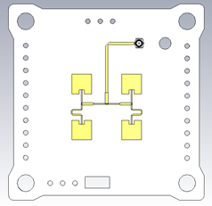
The last step in the design process of a 2x2 patch antenna is to design the entire feeding network and the patches distribution. Knowing this field has been exhaustively studied, some made designs were considered at the beginning of this project, and researching about this technology, a design of a 24 GHz lineally polarized patch antenna, with the inset impedance matching technique, was found in an online repository from Zhengyu Peng, Ph.D. (Texas Tech University). In this manner, a reverse engineering study has been carried out to understand this design and then adapt it further to our requirements.
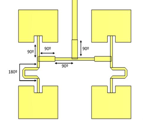
Array model and electrical lengths of the feeding network:
By adding an extra 180º length to access the patches from the bottom of the structure, the waves from the two resonant elements are adding up to each other. In addition, the corner mitering technique has been used as well.
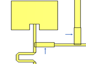
Mitred bend:
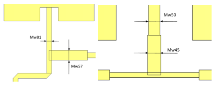
A 90º bend in a transmission line adds a small amount of capacitance to the transmission line, which causes a mismatch. A mitred bend as shown in the previous figure reduces some of that capacitance, restoring the line back to its original characteristic impedance. On the other hand, the whole structure impedance matching is done by two quarter-wave impedance transformers, adjusting the trace’s width to obtain the desired characteristic impedance that sets 50 Ω at the output of the network.
λ/4 impedance transformers:
The λ/4 impedance transformer design equation is included below, where Z0 is the characteristic impedance of the line, Zin the input impedance and ZL the impedance of the load.
Each line has been designed to match this equation according to the required input and output impedance:
- Mw45: 45 (Ω)
- Mw50: 50 (Ω)
- Mw57: 57 (Ω)
- Mw81: 81 (Ω)
CONNECTOR
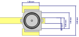
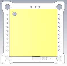
The antenna will be positioned on the upper side of the satellite. Therefore, the dimensions of the substrate layer are determined by the PoCat's own dimensions, which measure 40x40 mm². To enable the assembly of the entire structure, the payload's board includes holes for pins and screws. Additionally, a HIROSE C.FL connector is attached to the top section of the structure, where it connects to the 50 Ω feeding line. This allows easy access for the coaxial cable to connect to the upper layer from below, requiring the incorporation of a hole into the substrate and ground plane, placed at the farthest point compatible with elements from payload 2.
Connector mounting pattern following HIROSE’s recommendation:
FINAL 2X2 PATCH ANTENNA ARRAY MODEL





No Comments