Subsystem Verification (SSV)
DOCUMENT SCOPE
The aim of this document is to explain the subsystem verification tests to carry out on Attitude Determination & Control Subsystem, in order to obtain/discard any anomaly that the subsystem could suffer during the performance of these test.
TEST 1: Electrical check
Test Description and Objectives
The aim of this test is to verify that none of the components or connections were damaged during assembly, ensuring the integrity and reliability of the board. This involves checking for any physical defects or misalignments that could impact performance, as well as measuring electrical parameters to ensure that the components operate efficiently. Conducting this test helps to identify any potential issues that could lead to failure in the field, thereby ensuring the overall functionality and longevity of the assembled device.
Requirements Verification
| Requirement ID | Description |
|---|---|
| ADCS - SSV - 00 | All external physical aspects, such as scratches, soldering, or joint issues, of the PCB must be inspected. |
| ADCS - SSV - 01 | Each lateral pin must establish a secure connection. |
| ADCS -SSV - 02 | All active components must be ensured to operate correctly, with no short circuits or open connections, and each pin, must meet the specified value. |
| ADCS -SSV - 03 | The positioning and fitment of each component mounted on the PCB must be verified. |
Test Set-Up
- ADCS payload full soldered
- Microscope
- Power Supply
- Wires
- Soldering machine
- Tin
- Flux
- Multimeter
- Calculator, pen and paper
- Laptop
Pass/Fail Criteria
In order to pass the test all the requirements must be met.
Test Plan
| **Step ID** | **Description** |
| Test1 - 10 | With the help of the microscope, look at the PCB looking for any outer physical parameters, such as scratches, soldering or joint issues. If any anomaly is detected, re-solder or fix the encountered error. |
| Test1 - 20 | Check the correct connection with the corresponding component of the 40 pins (10 in each lateral side) with the multi-meter. |
| Test1 - 30 | Check the value with the multi-meter of all the passive components and compare it to the one in the schematic. |
| Test1 - 40 | Verify the active components, checking one by one all the pins with the multi-meter in order to find shorts, open ends, and correct connections among the various pins. |
| Test1 - 50 | Check the connections between all of the components and pins of the PCB. |
Test Results
The test for the ADCS PCB has been done during the 09/03/2023.
The test passed the visual inspection since the outer physical checking was successful.
The pins', passive and active components' connectivity were successfully accomplished considering that there were no open ends or shorts, and the component values were correct.
The in-circuit testing was passed since the connections between all of the components and pins of the PCB were verified.
Anomalies
Power Supply problems
Problem encountered: When putting the 3.3V into the 3.3_PERM pin of the PCB, the voltage measured in the pin is not 3.3V. Follow these steps:
- Check the board again with the multimeter searching for any short circuit
- Check the schematic to see if there is any mistake
- If not anomalies are detected, resolder the PCB
Solution:
Once the first two points were made and since the problem was no resolved it became necessary to desolder certain blocks of the PCB, with the operational amplifiers being the first among them. After removing the amplifiers the voltage was tested using a multimeter, marking the needed 3.3V.
Conclusions
The PCB passed the electrical test and is ready to do more complex tests.
TEST 2: GYROSCOPE
Test Description and Objectives
The purpose of this test is to validate that the gyroscope integrated into the PCB operates in accordance with the specified requirements and successfully communicates with the computer using the I2C protocol. This includes assessing the gyroscope's performance metrics and ensuring reliable data transmission between the gyroscope and the computer.
Requirements Verification
| Requirement ID | Description |
|---|---|
| ADCS - SSV - 10 | The gyroscope must be tested using a reliable tool capable of reproducing constant angular velocities accurately. |
| ADCS - SSV - 11 | The gyroscope must be able to switch between specific full scale ranges of angular velocities. |
| ADCS - SSV - 12 | The gyroscope produced bits, must be translated in degrees per second or radians per second. |
| ADCS - SSV - 13 | The data from the gyroscope must closely match the theoretical value corresponding to the rotation of the rotary platform. |
Test Set-Up
- ADCS PCB
- STM32L476RG nucleo board
- Power Supply
- Wires
- Multimeter
- Oscilloscope
- Calculator, pen and paper
- Reliable tool capable of reporducing constant angular velocities. In example a rotating platform with motor.
- Power supply.
- Chronometer, you can use a mobile application
- Desired programming software used, in this test STM32CubeIDE is used
Pass/Fail Criteria
The gyroscope will be verified if the requirements mentioned before are fulfilled. If in one of them it is detected any anomaly it will have to be corrected, otherwise the board can not pass to the other tests.
Test Plan
| **Step ID** | **Description** |
| Test2 - 10 | Connect the power supply to the STM32 nucleoboard. |
| Test2 - 20 | Open the STM32CubeIDE program. |
| Test2 - 30 | Prepare a code that can read from the gyroscope using I2C. |
| Test2 - 40 | Connect the nucleoboard to the ADCS PCB correctly. |
| Test2 - 50 | Run the code into the nucleoboard in the debug mode checking step by step if the connection with the ADCS board is working correctly. |
| Test2 - 60 | Connect the rotating platform with motor to the power supply, inject the voltage and intensity needed for the proper operation of the engine. |
| Test2 - 70 | Place the gyroscope in the rotation platform and run the code. Write down the values of the data. |
| Test2 - 80 | Measure with the chronometer how long the platform takes in rotating 360 degrees, then compute how many degrees per second it is equivalent to. |
| Test2 - 90 | If the values of the gyroscope and the computed value corresponds with the values computed before, the gyroscope is working correctly. |
3.5.1 I2C communication and registers
The device address of the IIM-42652 is AD = 0b1101000X where the last bit "X" is chosen depending in what function we are conducting in the chip register, reading X=1 or writing X=0.
The registers modified and used in the code are the following ones:
| **REGISTER NAME** | **ADDRESS** | **FUNCTION** |
| SENSOR\_CONFIG0 | 0x03 | Disables and enables the gyroscope axis. |
| PWR\_MGMT0 | 0x4E | Enables and disables all sensors of the chip. We are only enabling the temperature sensor and the gyroscope. |
| GYRO\_CONFIG\_STATIC2 | 0x0B | Disables and enables Anti-Aliasing/low pass filter and notch filter. In our case we are using only the Anti-aliasing and low pass filter. |
| GYRO\_CONFIG0 | 0x4F | Configuration register for the gyroscope, the full scale range and the ODR frequency can be modified. We are using the default frequency of the ODR and a full scale range that fluctuates depending on the situation (this can't be configurated via registers, it has to be coded). |
| GYRO\_DATA\_X1/X0 | 0x25/0x26 | X1: Upper byte of Gyro X-axis data. X0: Lower byte of Gyro X-axis data. |
| GYRO\_DATA\_Y1/X0 | 0x27/0x28 | X1: Upper byte of Gyro Y-axis data. X0: Lower byte of Gyro Y-axis data. |
| GYRO\_DATA\_Z1/X0 | 0x29/0x2A | X1: Upper byte of Gyro Z-axis data. X0: Lower byte of Gyro Z-axis data. |
| TEMP\_DATA1/0 | 0x1D/0x1E | X1: Upper byte of temperature data. X0: Lower byte of temperature data. |
For more information about I2C and registers read the datasheet of the IIIM-42652.
An implementation of a register reading:
    /*Device address*/
    uint8_t IIM_GYRO_ADR = 0x68;
    /*Device actions*/
    uint8_t IIM_GYRO_READ = (0x68 <<1)|0x1
    uint8_t IIM_GYRO_WRITE = (0x68 <<1)
    /*Registers addresses*/
    uint8_t GYRO_DATA_X1_UI = 0x25;
    /*Data buffer declaration*/
    uint8_t buflenght =6;
	uint8_t buf[buflenght];
    /*Config register of the chip*/
    buf[0]=GYRO_DATA_X1_UI;
    /*I2C Transmision*/
    HAL_I2C_Master_Transmit(status.i2c_h, IIM_GYRO_WRITE, buf,1,HAL_MAX_DELAY );
    /*I2C Reception*/
    HAL_I2C_Master_Receive(status.i2c_h /*I2C pointer*/ ,IIM_GYRO_READ,buf,1,HAL_MAX_DELAY);
An implementation of a register writing:
    /*Device address*/
    uint8_t IIM_GYRO_ADR = 0x68;
    /*Device actions*/
    uint8_t IIM_GYRO_READ = (0x68 <<1)|0x1
    uint8_t IIM_GYRO_WRITE = (0x68 <<1)
    /*Registers addresses*/
    uint8_t PWR_MGMT0 = 0x4E;
    /*Register modifications*/
    uint8_t SET_GYRO_LOWNOISE_MODE = 0x0C;
    /*Data buffer declaration*/
    uint8_t buflenght =6;
	uint8_t buf[buflenght];
    /*Bits to modify in the register*/
    buf[0]=PWR_MGMT0;
    buf[1]=SET_GYRO_LOWNOISE_MODE;
   /*I2C Transmision*/
  HAL_I2C_Master_Transmit(status.i2c_h/*I2C pointer*/, IIM_GYRO_WRITE, buf,2,HAL_MAX_DELAY);
3.5.2 Data acquisition
The output of the gyroscope only give us an integer of 16 bites. In order to convert the integer into data, you have to divide the integer, where you have stored the data of the axis, by the sensitivity scale factor corresponding to the full-scale range that is used to measure the current data. The result will be the gyroscope rotation in degrees/second.
Test Results
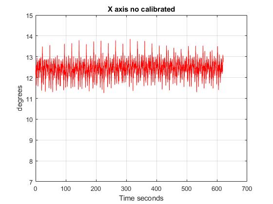
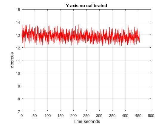
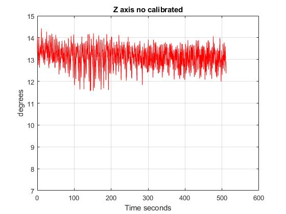
The following data has been obtained in each axis of the gyroscope:
The obtained data is not calibrated, therefore, a calibration test has been made.
Conclusions
With all requirements met, the gyroscope has successfully passed the test, and the ADCS PCB is now prepared for further testing.
TEST 3: Magnetometer
Test Description and Objectives
The purpose of this test is to validate that the Magnetometer integrated into the PCB operates in accordance with the specified requirements and successfully communicates with the computer using the I2C protocol. This includes assessing the Magnetometer's performance metrics and ensuring reliable data transmission between the Magnetometer and the computer.
Requirements Verification
| Requirement ID | Description |
|---|---|
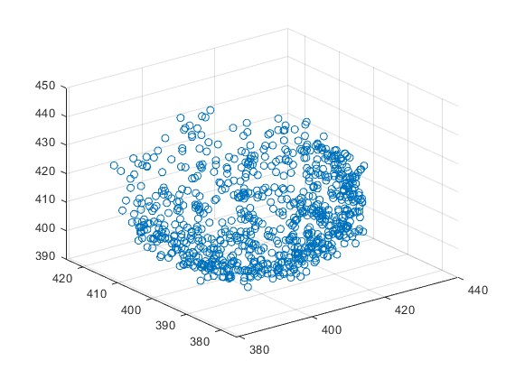
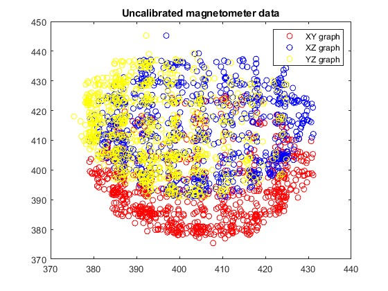
| ADCS - SSV - 20 | The magnetometer data for each axis should display an elliptical shape. |
| ADCS - SSV - 21 | Test measurements should be conducted in an area free from any potential magnetic sources. |
Test Set-Up
- ADCS PCB
- STM32L476RG nucleoboard
- Power Suppply
- Wires
- Multimeter
- Oscilloscope
- Calculator, pen and paper
- Laptop
- Magnet
Pass/Fail Criteria
The magnetometer will be verified if the requirements mentioned before are fulfilled. If in one of them it is detected any anomaly it will have to be corrected, otherwise the board can not pass to the other tests.
Test Plan
| **Step ID** | **Description** |
| Test3 - 10 | Prepare the power supply with 3.3V and 800mA. |
| Test3 - 20 | Connect the power supply to the PCB. |
| Test3 - 30 | With the help of the multimeter, check that the VCC inputs pins has the correct value. |
| Test3 - 40 | Disconnect the power supply and turn it off. |
| Test3 - 50 | Turn on the computer and open the STM32CubeIDE program. |
| Test3 - 60 | Prepare a code that can read from the magnetometer using I2C. |
| Test3 - 70 | Connect the nucleoboard to the ADCS PCB using SCL and SDA pins. |
| Test3 - 80 | Run the code into the nucleoboard and look in the memory register to see if the communication between the nucleo and the PCB has been done. |
| Test3 - 90 | Run again the code and conduct measurements of the magnetometer being rotated randomly to all directions. |
4.5.1 I2C communication and registers
The device address of the MMC5983MA chip is the AD=0b0110000. The following registers are modified and used in the code:
| **REGISTER NAME** | **ADDRESS** | **FUNCTION** |
| Internal Control 0 | 0x09 | This register is mainly used for initiating a measurement event of the magnetic field or the temperature. Among other things. |
| Status | 0x08 | This register is used for checking if the measurement event of the magnetic field or the emperature, is completed. |
| Xout0, Yout0, Zout0 | 0x00, 0x02, 0x04 | X,Y,Z-axis output in unsigned format. Bits \[17:10\] |
| Xout1, Yout1, Zout1 | 0x01, 0x03, 0x05 | X,Y,Z-axis output in unsigned format. Bits \[9:2\] |
| XYZout2 | 0x06 | X,Y,Z-axis output in unsigned format. Bits \[1:0\] |
For more information about I2C and registers read the datasheet of the MMC5983MA .
4.5.2 Data acquisition
The registers will provide a 18 bits number. This
3.5.2 I2C Problem
5. Posible errors
If the error is in the Start Flag of the I2C communication, check if you are using the correct hi2c Pointer to a I2C_HandleTypeDef structure that contains the configuration information for the specified I2C.
If the error is in the Stop Flag of the I2C communication, the ADCS board is not responding, follow the steps of the section
Test Results
The obtained data is not calibrated, therefore, a calibration test has been made.
Anomalies
With the electrical test complete and all hardware functioning properly, if measurements remain unchanged or varely do not change. Try exciting the magnetometer with a magnet. Bring the magnet close to the magnetometer chip and rotate the PCB randomly. This should resolve the issue.
Conclusions
With all requirements met, the gyroscope has successfully passed the test, and the ADCS PCB is now prepared for further testing.
TEST 4: Photodiode and Operational Amplifiers
Test Description and Objectives
The purpose of this test is to validate that the Photodiodes integrated into the lateral boards operate in accordance with the specified requirements. The Photodiodes block include the Operational amplifiers and also the photodiode multiplexer. The test involves evaluating the performance metrics of the photodiode and ensuring dependable data transmission between the magnetometer and the computer.
Requirements Verification
| Requirement ID | Description |
|---|---|
| ADCS - SSV - 30 | The photodiodes must only generate current proportional to the exposed light source. If there is no light source the photodiode must not generate any current. |
| ADCS - SSV - 31 | The operational amplifiers must convert the provided intensity of the photodiodes into voltage and amplify the signal. |
| ADCS - SSV - 32 | The analog to digital converter of the STM32 must convert the output of the operational amplifiers into bits. |
Test Set-Up
- ADCS PCB
- Photodiodes
- Multimeter, alligator clips ,cables and jumpers for the connection between the photodiodes and the ADCS board.
- Power supply
- A computer
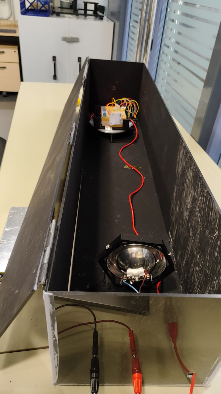
- Black coated box.
- An halogen bulb with its correct power source.
- Rotating platform.
Test Plan
| **Step ID** | **Description** |
| Test4 - 10 | Prepare the black coated box with the halogen bulb inside in one side of the box. |
| Test4 - 20 | On the other side prepare the photodiode on the rotating platform pinting towards the halogen bulb. |
| Test4 - 30 | Turn on the bulb and measure the output value with the help of a multimeter. |
| Test4 - 40 | Connect the photodiode to the operational amplifier and repeat stem 3. |
| Test4 - 50 | Connect the rotating platform to a power supply and do a complete round measuring the data and storing it in the computer. You can use the Analogic inputs from the STM32 board. |
| Test4 - 60 | Repeat the previous step, but in this case with the platform rotating in the opposite direction. |
| Test4 - 70 | Repeat step 4. and 5. rotating the photodiode 90 degrees. |
| Test4 - 80 | Plot the results. |
Connection schematic
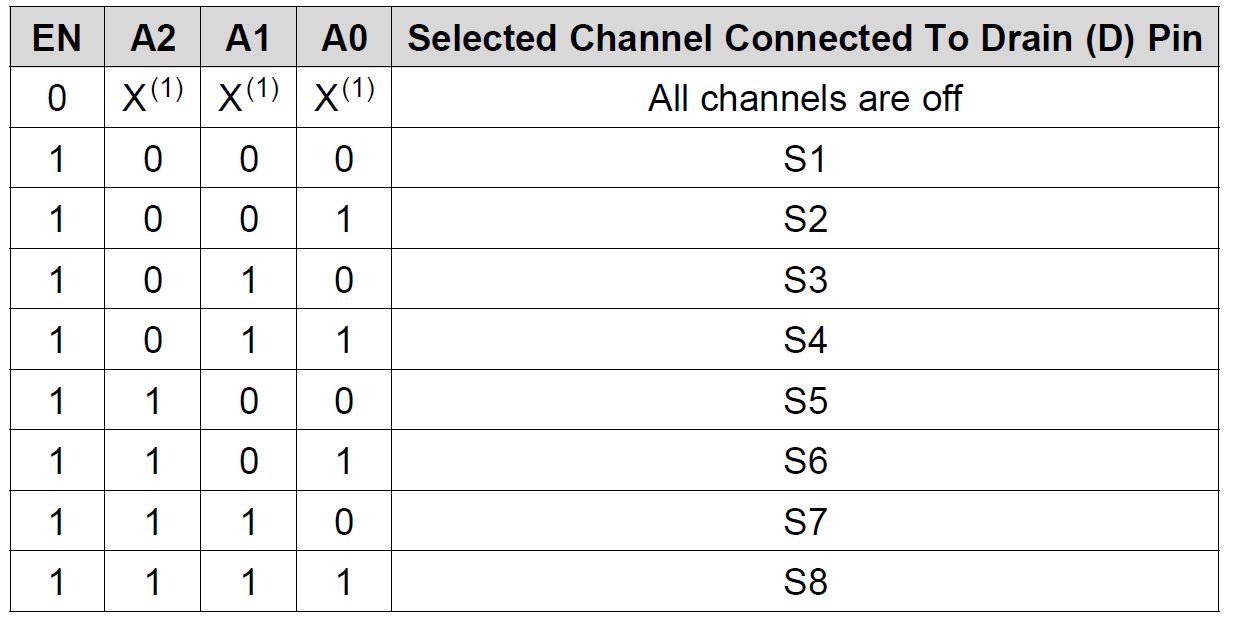
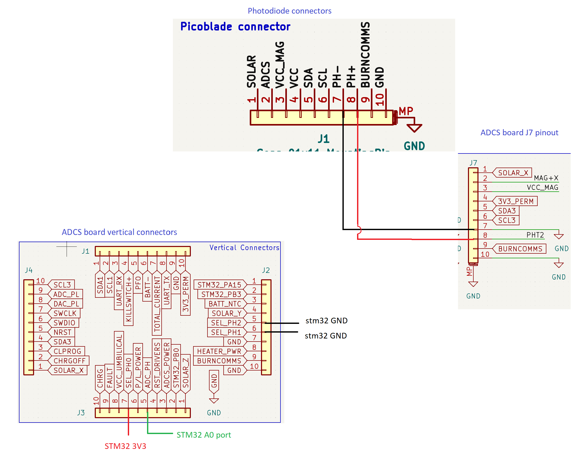
The schematic is simple, the pinouts SEL_PH from the vertial connectors of the ADCS board control the photodiode multiplexer. In the following picture you will have the truth table of the photodiode multiplexer used:
Pin A0 corresponds to SEL_PH0, A1 to SEL_PH1, and A2 to SEL_PH2. For this test, the output required is S2.
Test Results
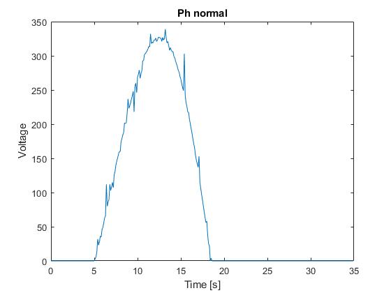
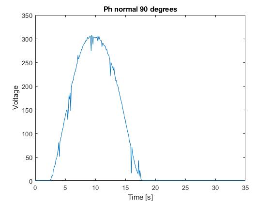
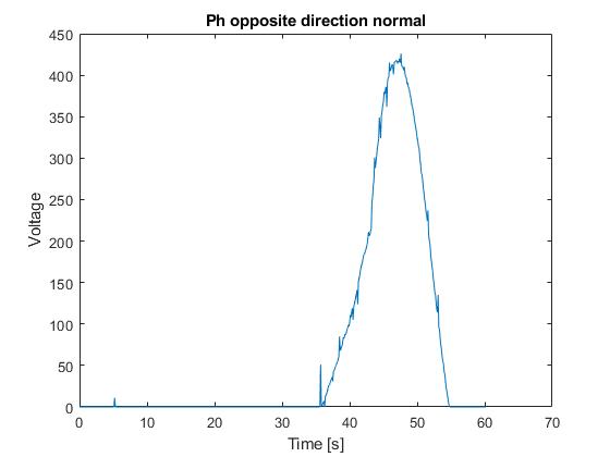
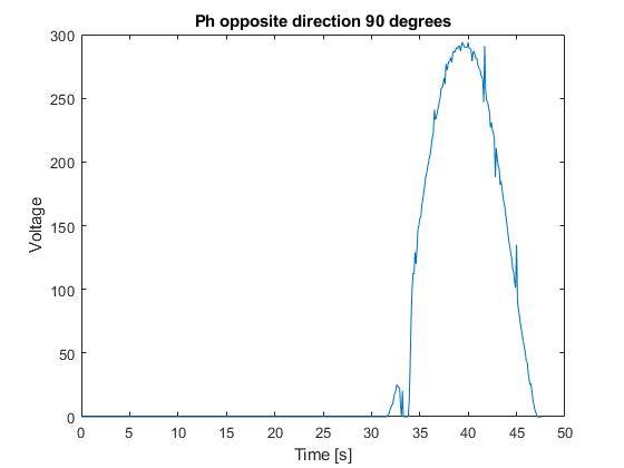
In this test, data was measured with a sampling frequency of 100 milliseconds, and the power supply for the rotating platform was set to 2.4 volts. The Y-axis represents the voltage levels recorded and quantified by the STM32, while the X-axis indicates time in seconds.
Regarding the plots, it can be observed that the photodiodes generally measure similar maximum power gains. However, in the bottom left plot, where the photodiode is oriented in the opposite direction of rotation at 0 degrees, the maximum power detected is significantly higher than in the other cases.
Anomalies
INo anomalies has been found in the test.
Conclusions
The photodiode and operational amplifier have fullfilled all the requirements so that, the test has been completed.
TEST 5: Magnetorquer actuator
Test Description and Objectives
The aim of this test is to verify that when the computer communicates with the magnetorquer actuator, specifying a current and the output pin, the output value of this block generates a constant current flow with the value and in the output pin what it was specified.
Requirements Verification
| Requirement ID | Description |
|---|---|
| ADCS - 31 | Sensor correctly supplied with 3.3V |
| ADCS - 32 | The device need to establish a connection with the computer using I2C |
| ADCS - 33 | The output values of the magnetorquer actuator block must be a constant current, with the specified value |
Test Set-Up
- ADCS payload
- STM32L476RG nucleoboard
- Protoboard
- Resistances of 10K, 20K and 30K Ohm
- Power Suppply
- Wires
- Multimeter
- Oscilloscope
- Mobile Phone
- Calculator, pen and paper
- Laptop with STM32CubeIde and Ki-Cad installed
Pass/Fail Criteria
The magnetorquer actuator block will be verified if the requirements mentioned before are fulfilled. If in one of them it is detected any anomaly it will have to be corrected, otherwise the board can not pass to the other tests.
Test Plan
| **Step ID** | **Description** |
| Test5 - 10 | Prepare the power supply with 3.3V and 800mA. |
| Test5 - 20 | Connect the power supply to the PCB using the ADCS\_POWER input. |
| Test5 - 30 | With the help of the multimeter, check that the VCC inputs pins has the correct value. |
| Test5 - 40 | Disconnect the power supply and turn it off. |
| Test5 - 50 | Turn on the computer and open the STM32CubeIDE program. |
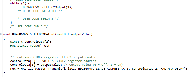
| Test5 - 60 | Prepare a code that can configure the output values and pins of the BD2606MVV. |
| Test5 - 70 | Connect the nucleoboard to the ADCS PCB using SCL and SDA pins. |
| Test5 - 80 | Run the code into the nucleoboard and look that the write and read functions return a "HAL\_OK" value, confirming the correct communication. |
| Test5 - 90 | Disconnect the nucleo board. |
| Test5 - 100 | Connect a protoboard to the output LEDA1 and to the 10K Ohms resistance. |
| Test5 - 110 | Prepare the code in order to configure the output with 1 mA and to the output LEDA1. |
| Test5 - 120 | Connect the nucleo board and run the code. |
| Test5 - 130 | With the help of the multimeter validate that the current is 1 mA. |
| Test5 - 140 | Disconnect the nucleo board and change the resistance to the 20 Ohms one. |
| Test5 - 150 | Connect the nucleo board and run the code. |
| Test5 - 160 | With the help of the multimeter validate that the current is still 1mA. |
| Test5 - 170 | Repeat the same process with the 30 Ohms resistance. |
| Test5 - 180 | Repeat the steps from 9 to 17 with the 6 outputs and for current valors of 10 mA, 20 mA and 35 mA. |
3.5.1 Code
The first thing that it is necessary to look at is the device address of BD2606MVV. This address can be found in page 7 of its datasheet or in the I2C address map from the nanosatlab wiki. This address is the "1100110". In the register map on page 8 of the datasheet it can be seen the memory register address for the configuration of the output pins:
LEDA1: 0x03, Data: D0 LEDB1: 0x03, Data: D2 LEDC1: 0x03, Data: D4
LEDA2": 0x03, Data: D1 LEDB2": 0x03, Data: D3 LEDC2": 0x03, Data: D5
In the same page it can be seen the address for the current settings of the leds output:
Lastly, on page 9 of the datasheet it is shown a with the address to configure the current value.
The protocol that it is followed by the device is the basic protocol on the I2C communications :
A possible code implementation is the following one:
3.5.2 I2C Problem
There is a problem with the I2C communication that makes the code fail. To solve this problem the next tests has been done:
1. Verify the connections
All the I2C connections are well connected with the corresponding PINS
2. Check the components
The components connected are the corresponding ones and in the correct positions according to the Ki Cad schematic. Furthermore no component has any short circuit.
3. Verify the addresses of the device
The device address is the correct one. It can be seen in the I2C Addresses document of the nanosatlab wiki or in the datasheet of the device
4. Check step by step that all the connections are working fine
- Disconnect the intern pull up / pull down resistances of the nucleoboard and connect it in a protoboard with a value of 20K ohms. Check now the SCL transmission with an oscilloscope
- The SCL signal was correctly seen in the oscilloscope
- Check now the SDA transmission and check that it is transmitting the correct address of the sensor device
- The transmission of the SDA line, send by the nucleo board, is correct.
- Connect now the PCB, if it do not have its own pull up resistance connect it using the protoboard and the 20Kohms resistances.
- With the oscilloscope check if the device is responding The device is not responding with the expected ACK
Test Results
Anomalies
The anomalies detected during this test is the I2C problem, that are explained in detail in 3.5.2
Conclusions
This test remains to be redone with a more deeply debug proce

