Hardware Tests as Run
DOCUMENT SCOPE
The aim of this document is to clearly explain the tests performed during the delevolpment of the subsystem.
This document is based on current but also previous versions both of hardware and software and as such be followed with care.
ANTENNA MATCHING TEST
Test Description and Objectives
Antenna impedance matching is a crucial aspect in the design and operation of radio frequency systems. Impedance matching involves adjusting the impedance of the antenna to match the impedance of the transmission line or the RF source to which it is connected. The objective of the test will be to determine the length of the quarter wavelength monopole antenna for the satellite.
Requirements Verification
| Requirement ID | Description |
|---|---|
| AMT - 01 | The antenna should exhibit impedance values closely matching the specified target impedance across the defined frequency range (868 MHz). |
| AMT - 02 | Return loss values should be high, indicating a low amount of power reflected back towards the source and efficient power transfer. |
| AMT - 03 | The antenna should demonstrate acceptable impedance matching and performance across the specified bandwidth(125kHz). |
Test Set-Up
Materials:
- Vector Network Analyzer (VNA)
- Coaxial Cables
- Antenna
- Computer
Setup
- Prepare the Testing Environment
- Connect the Vector Network Analyzer (VNA)
- Calibrate the VNA
- Connect Coaxial Cables
- Position and Orient the Antenna
Pass/Fail Criteria
| Parameter | Pass Criteria | Fail Criteria |
|---|---|---|
| Return Loss | Return Loss < -10 dB (lower values are better) | Return Loss > -10 dB (indicating poor matching) |
| Standing Wave Ratio (SWR) | SWR < 2:1 (lower values are better) | SWR > 2:1 (indicating poor impedance matching) |
| Impedance Matching | Impedance matched to system requirements | Significant deviation from desired impedance |
| Radiation Pattern (optional) | Symmetrical and aligned with specifications | Irregular pattern, beam tilting, or distortions |
Test Plan
| Step - ID | Description |
| AMT\_S-01 | Prepare the Testing Environment:
|
| AMT\_S-02 | Calibrate the Vector Network Analyzer:
|
| AMT\_S-03 | Connect the Antenna:
|
| AMT\_S-04 | Measure the Antenna Impedance:
|
| AMT\_S-05 | Analyze Measurement Results:
|
| AMT\_S-06 | Optimize and Fine-Tune (if needed):
|
| AMT\_S-07 | Save and Store Data:
|
Test Results
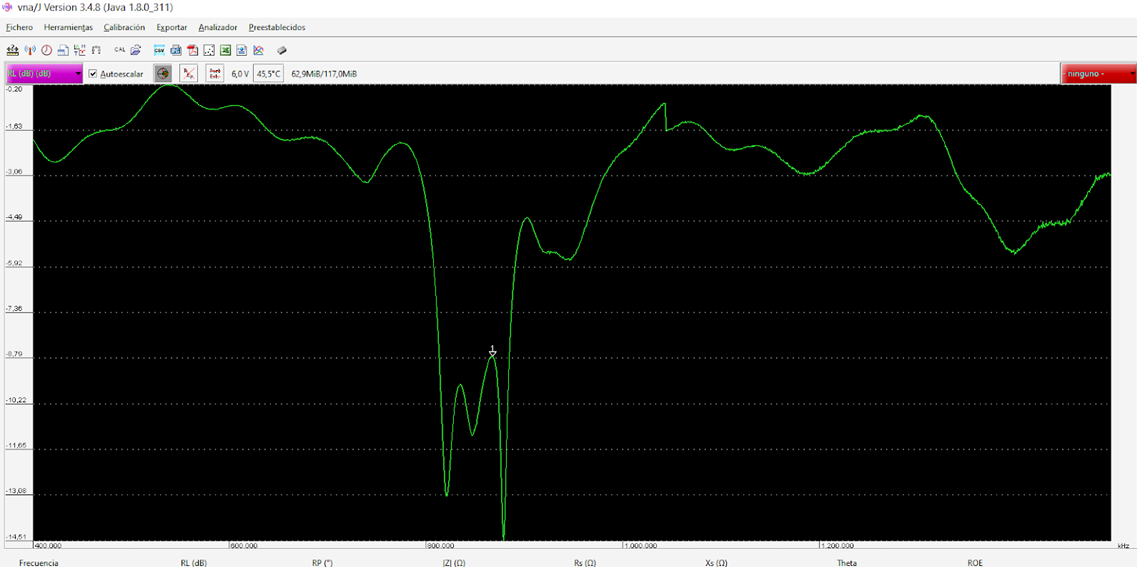
The test was conducted in the autumn of 2022, and the outcomes are as follows:
As can be seen in the figure above, the final antenna had RL(dB) = -10 for the operating frequency. Moreover, the bandwidth of the antenna is approximately 15 MHz.
The result obtained from this test, however, is quite surprising: the antenna length must be 3.5 cm, which is much lower than what was theoretically calculated (8.64 cm). The reason behind this result could be the non-ideal ground plane of the monopole.
Anomalies
Obtained antenna lenght is 3.5 cm, lower than what was theoretically calculated (8.64 cm).
Conclusions
Test should be redone with the final version of the PocketQube.
OBC-COMMS BOARD TEST
Test Description and Objectives
The objective of this test is to validate the correct operations of the COMMS layout in the PocketQube with the OBC&COMMS board.
Requirements Verification
| Requirement ID | Description |
|---|---|
| OCBT - 01 | Be able to see MISO, MOSI, SCK, SX1262-NSS, SX1262-NRST and SX1262-BUSY signals. |
| OCBT - 02 | Be able to decodify MISO, MOSI and SCK |
| OCBT - 03 | MISO, MOSI and SCK decodification must match expected results of the datasheet. |
Test Set-Up
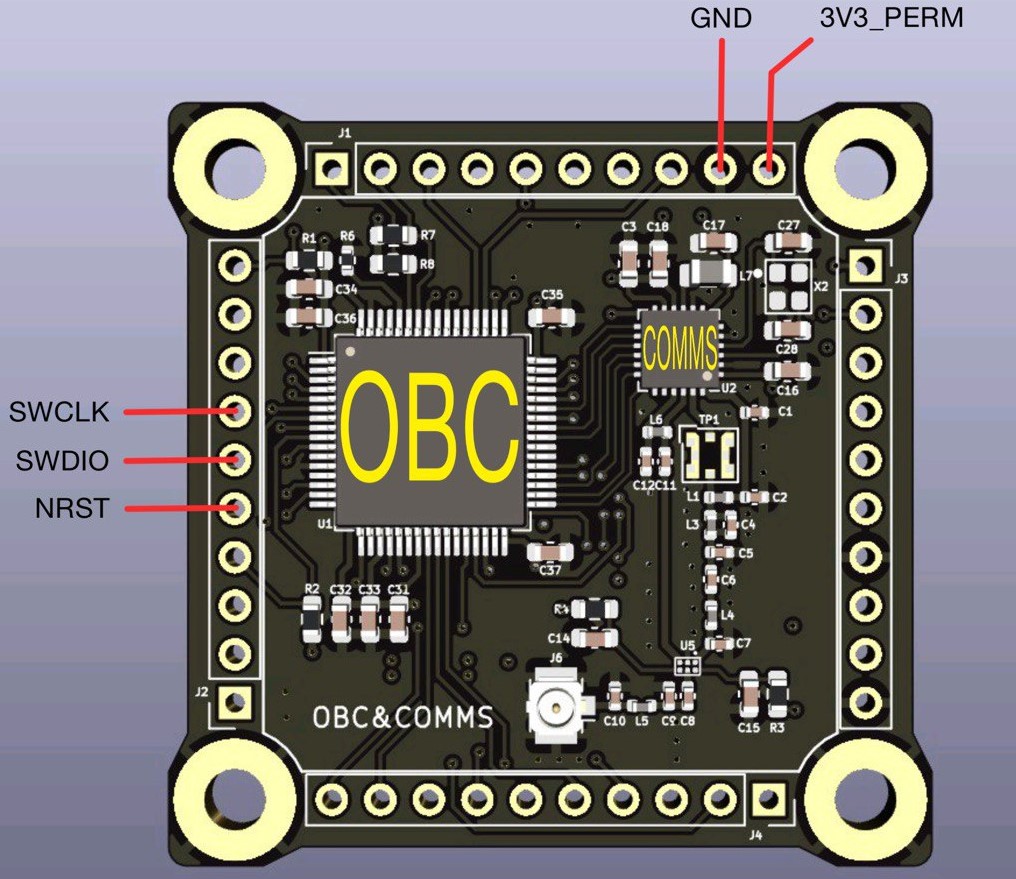
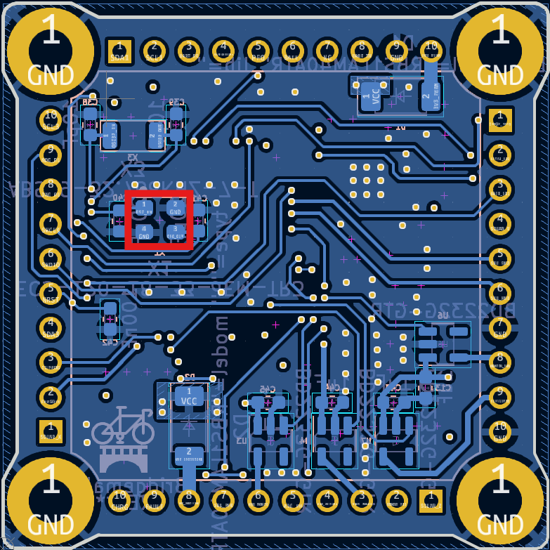
OBC&COMMS with only used pinouts:
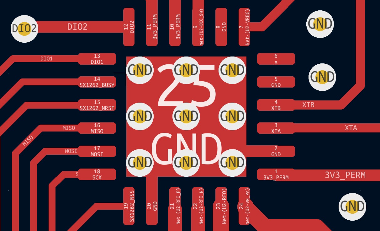
If we zoom into the COMMS chip we get the following:
We'll measure the following pins: MISO, MOSI, SCK, SX1262_NSS. These are the only ones available for comparison with the expected values outlined in the datasheet.
Materials:
- OBC&COMMS board
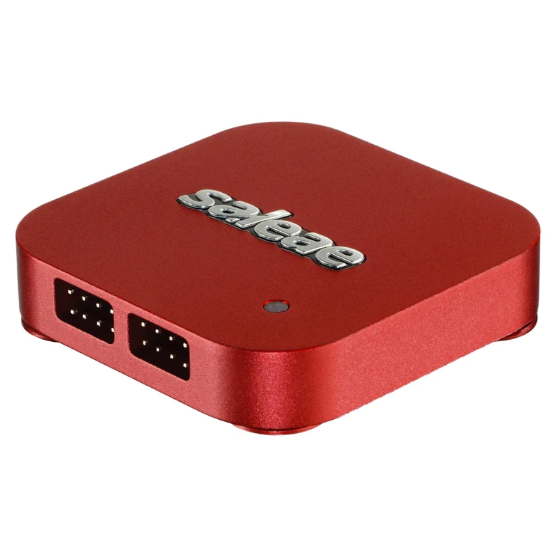
- Spectrum Analyzer (we used Saleae)
- Multiple Cable Jumpers
- PC with STM32Cube IDE installed
- Two 4.7K Ohms pull-up resistors
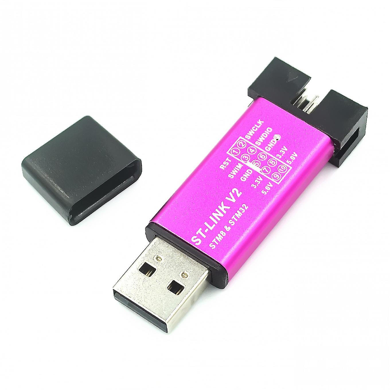
- ST-LINK v2
Setup
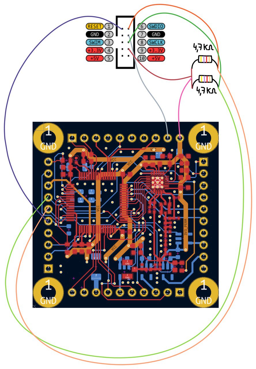
We will connect the ST-LINK v2 to a PC for flashing code. The SWDIO, SWCLK, and 3.3V ports of the ST-LINK v2 will link to pull-up resistors shown in the following image before connecting them to their respective pins. Meanwhile, the other ports (GND and RESET) will be directly linked to the board.
Pass/Fail Criteria
To verify the functionality of the COMMS chip, we'll compare the obtained results with the expected specifications outlined in the SX1262IMLTRT datasheet.
The test will be deemed successful if our obtained results align with those specified in the datasheet. If they don't correspond, the test will be considered unsuccessful.
Test Plan
| Step ID | Description | Pass/Fail Criteria | Actual | Passed(Y or N) |
| CS - 01 | Prepare the setup explained in the previous step | Flashing must be successful, a "successful message" must appear | We encountered a lot of issues when flashing due to poor connections, after many attemps we successfully flashed | Sometimes, had to repeat multiple times until it worked |
| CS - 02 | Flash code, we used the main program (Project>>Build All + Run>>Debug As>>1STM32C...) | |||
| CS - 03 | Using Saleae, check all pins of the SX1262 chip, especially MISO, MOSI, SCK and SX1262-NSS | Just after flashing we must see signals in all these pins | Only MISO had a visible signal, the others had not | No, no signal was spotted in MOSI, SCK and SX1262-NSS. |
| CS - 04 | Once we have simultaniously captured MISO, MOSI and SCK, decodify the signal | Comparing with the SX1262 datasheet, the decodification must be the one we expected | Since we only obtained the MISO signal, it has been impossible for us to decode | No |
Test Results
We encountered several issues while working on the project. Firstly, we faced weak connections between the board and the computer for CS-01 and CS-02, which resulted in several days of troubleshooting. We had to solder connectors to establish a stable connection, but the board remained fragile, and we couldn’t touch it much.
Moving on to CS-03, we encountered three major issues. The first issue was with the tool we used for decodification. We needed three ports to capture all three signals (MISO, MOSI, and SCK) simultaneously, so we had to switch from PicoScope to a Saleae device. The second issue was the small size of the chip and connections, which made it extremely difficult (if not impossible) to capture all signals simultaneously. We recommend adding testing pins to the board in future versions. Finally, the third issue was with the decodification process itself. We could only observe MISO, SX1262_NRST, SX1262_NSS, XTA, and XTB signals. Since we also needed MOSI and SCK signals to decode the signal, we were unable to do so. We also checked the power pins going to the SX1262 and found no issues.
As for CS-04, we were unable to compare it with the datasheet since we couldn’t decode it.
Anomalies
During the project, we faced several issues. As previously mentioned, we encountered anomalies during the test, including fragile connections, small pins on the chip that made it difficult to check all signals simultaneously, and no signal for MOSI and SCK. Unfortunately, we were unable to decode the signal.
Conclusions
As the COMMS subsystem relies heavily on this crucial test, essential for communication testing, we've opted to temporarily skip it. Instead, we will use a spectrum analyzer to verify if the chip is transmitting signals. If successful, it confirms effective communication between the OBC and COMMS chips. However, if no signals are detected, the issue may lie in the connections/design of the board.
RX-TX TEST
Test Description and Objectives
Due to the outcomes of the OBC-COMMS board test, an alternative method is required to validate ongoing communication between the OBC and COMMS chips. To achieve this, we plan to establish communication between a TinyGS and the OBC-COMMS board, effectively simulating the connection between a ground station and our satellite. Furthermore, attenuations will be introduced later in the process to mimic the conditions present in space.
Requirements Verification
| Requirement ID | Description |
|---|---|
| RXTX - 01 | Be able to transmit using a TinyGS. |
| RXTX - 02 | Be able to receive the transmitted data using the SX1262. |
| RXTX - 03 | Possess the capability to respond to specific telecommands by transmitting a reply. |
| RXTX - 04 | Have the capability to initiate communication between the TinyGS and the OBC-COMMS while incorporating attenuations. |
| RXTX - 05 | Possess the capability to process telecommands and provide responses while incorporating attenuations. |
Test Set-Up
Materials
- Computer with VisualStudio Code (with extension PlatformIO) and STM32CubeIDE
- STM-32 nucleo board
- LoRa module SX1262
- OBC-COMMS board
- TinyGS (868-915MHz LILYGO LoRa 32 v2)
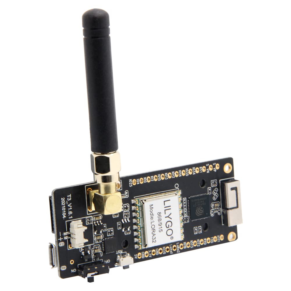
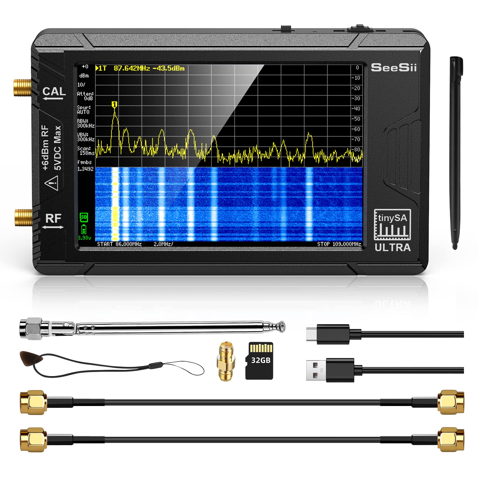
- TinySA Spectrum Analyser
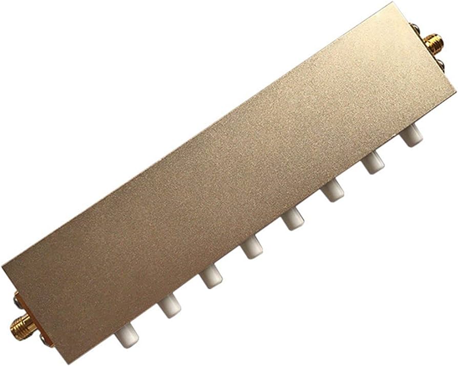
- BECEN SMA Female to Female 50 ohm Push-Button Step attenuator,Key-Press Attenuator,DC to 2.5GHz (90db)
Setup
For the initial and fundamental phase of our test, the setup is as follows:
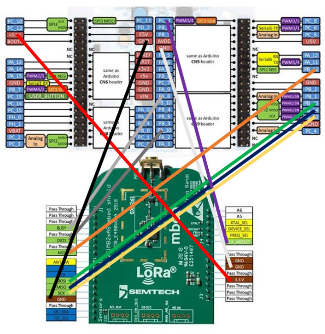
One computer will be connected to a TinyGS, while the other computer will have a Nucleo+LoRa module connected to it. This configuration allows us to verify the transmission capability of the TinyGS and the responsiveness of the board (initially represented by an STM32 Nucleo + LoRa module).
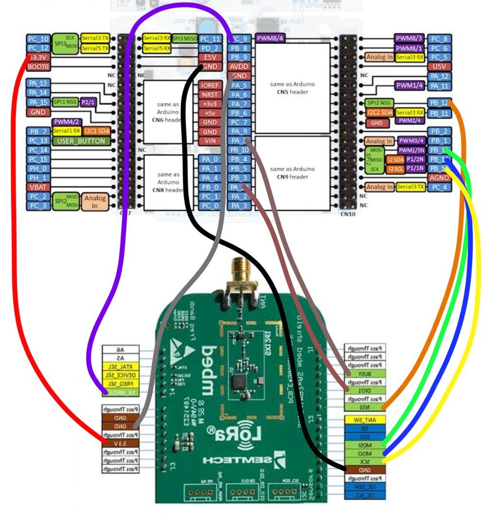
The setup for the STM32 Nucleo + LoRa module is the following:
After successfully testing this setup, the next configuration is as follows:
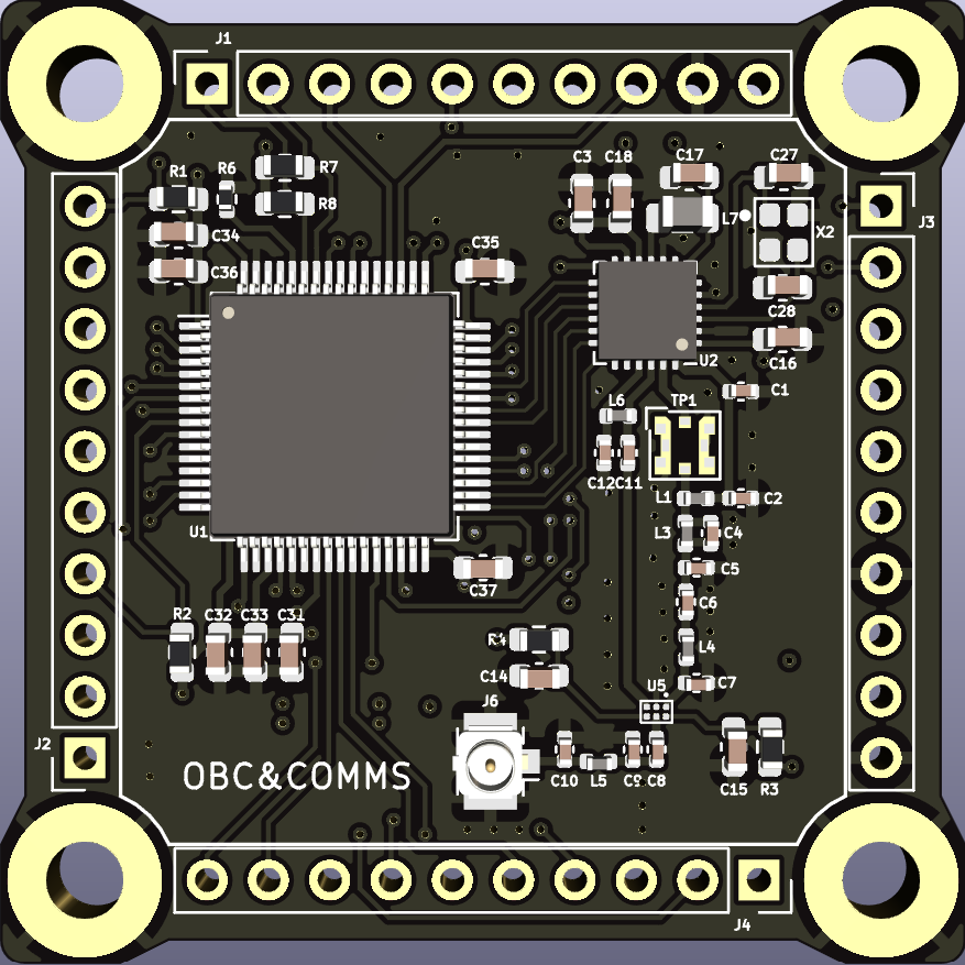
Instead of the Nucleo+LoRa, we will integrate the OBC-COMMS board from the OBC-COMMS board test.
As we advance in the testing process, we will introduce a variable attenuator in either reception or transmission.
Throughout the experiment, a spectrum analyzer will be employed to detect the signals transmitted, while the TinyGS console will be utilized to monitor both sent and received data.
Pass/Fail Criteria
The experiment will be deemed successful if the specified requirements are fulfilled, signifying our ability to transmit effectively using the TinyGS, and the OBC-COMMS board responds as anticipated, both in the presence and absence of attenuation.
Test Plan
Step 1: TinyGS configuration
The initial phase of this test involves configuring and preparing a TinyGS station. Since a similar station has been utilized in previous tests, please refer to the instructions provided in the "ᴾᵒCat Testing >> ᴾᵒCat SSVs >> COMMS Software SSV" section for guidance.
Step 2a: TinyGS transmission
Once our TinyGS is configured we can test its transmission capabilities by sending one of the telecommands shown in the TinyGS console. For checking the correct transmission we will used a spectrum analyser. 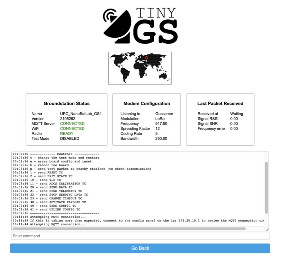
Step 2b (optional): TinyGS to TinyGS
If encountering transmission difficulties, we can attempt communication between two TinyGS units. This approach allows us to showcase the capability of our TinyGS in both sending and receiving data. The necessary steps involve configuring a second TinyGS (just like we did with the first one) and issuing a telecommand, with the option to utilize the "p" command for sending a test packet.
Step 3: STM32 + LoRa
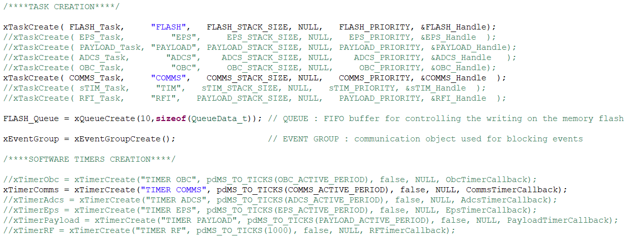
Upon confirming the proper functionality of the TinyGS, the next step is to connect the STM32 Nucleo + LoRa module to the computer. Subsequently, we will flash our code into it to activate the reception mode of the SX1262 (LoRa module). Finally, we will initiate transmission using the TinyGS and observe if the STM32+LoRa module responds. For this test we will only take into account the "FLASH" and "COMMS" tasks.
Step 4: Board
After confirming the correct functionality of the code on the STM32 Nucleo + LoRa module, we can proceed to the next stage of utilizing the board. If the preceding tests yield success, but this phase encounters issues, we can confidently conclude that the issue lies in the hardware rather than the software, thereby narrowing down the potential sources of errors.
Step 5: Attenuations
If all the preceding steps are successful, the next phase involves experimenting with attenuators to simulate the conditions our system will encounter in space. Common attenuators and a variable attenuator will be employed for this purpose. The objective of this step is to assess the feasibility of transmission under various influencing factors such as distance, speed, angle of the antennas, and other relevant parameters.
Test Results
Step 1:
The configuration of the TinyGS for transmission and reception at 868MHz was completed successfully.
Step 2a/2b:
The TinyGS exhibits the ability to both transmit and receive data, as exemplified by the successful demonstration using two TinyGS units. In the event of possessing only one TinyGS, we can showcase the effective operation of the ground station by employing a spectrum analyzer and receiving signals from satellites that are using the TinyGS network.
Step 3:
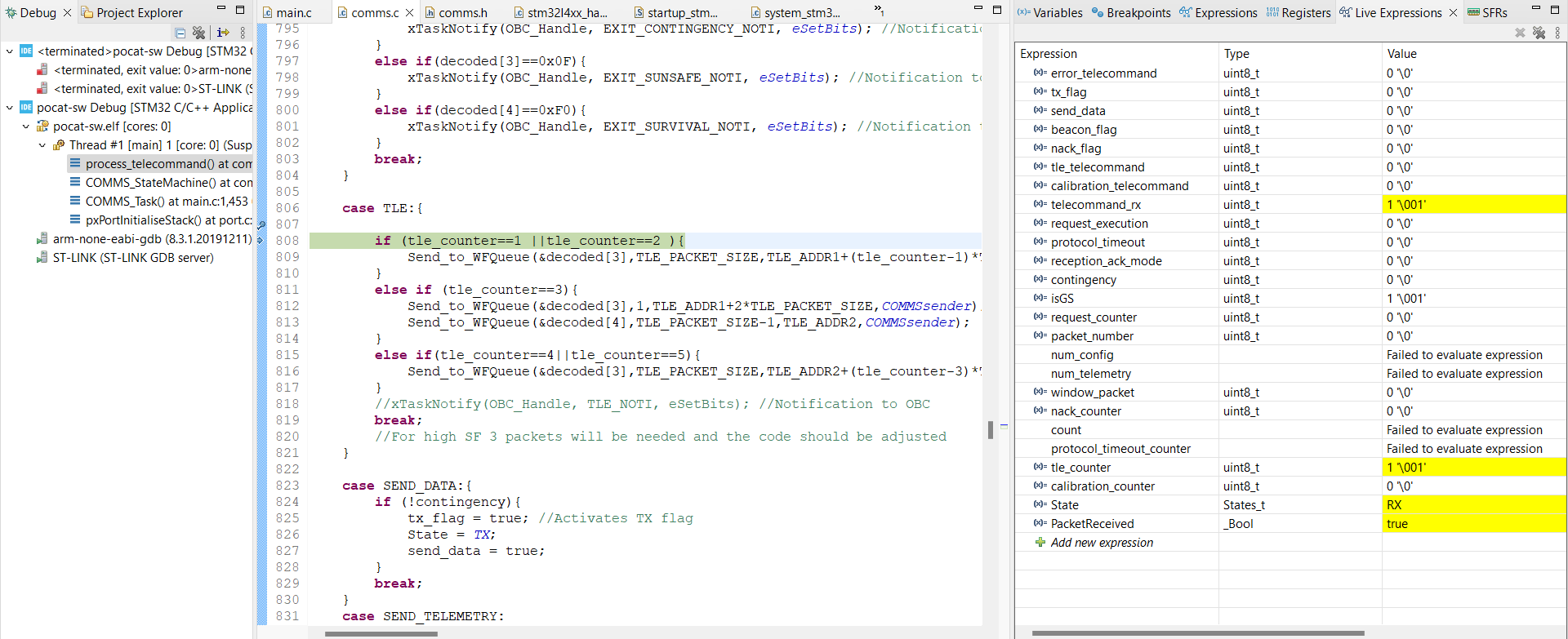
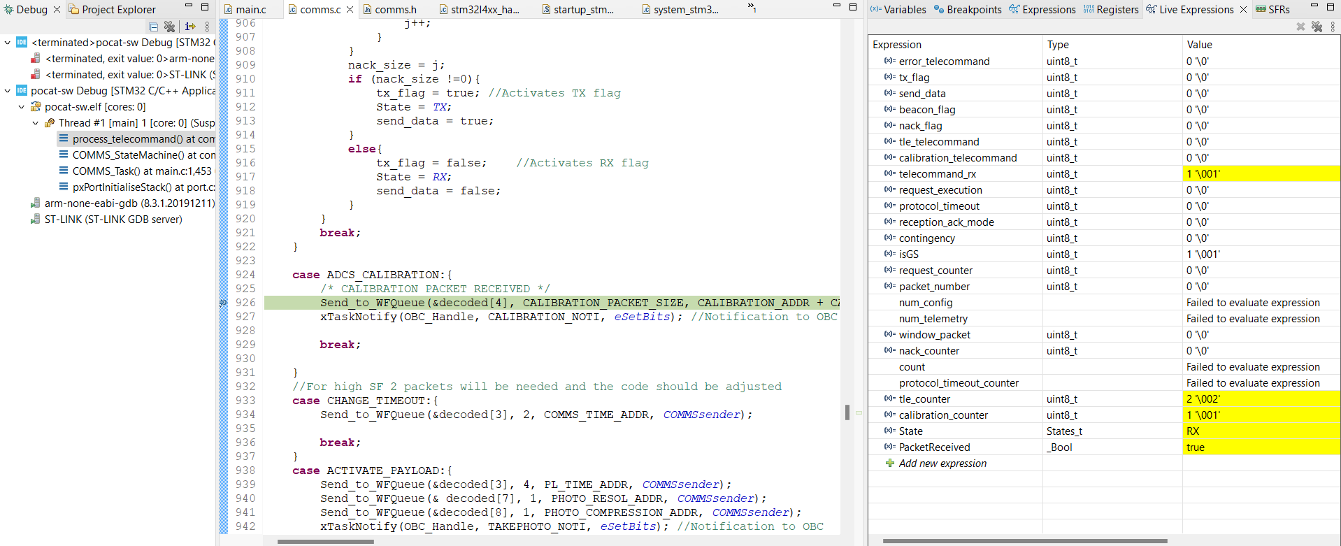
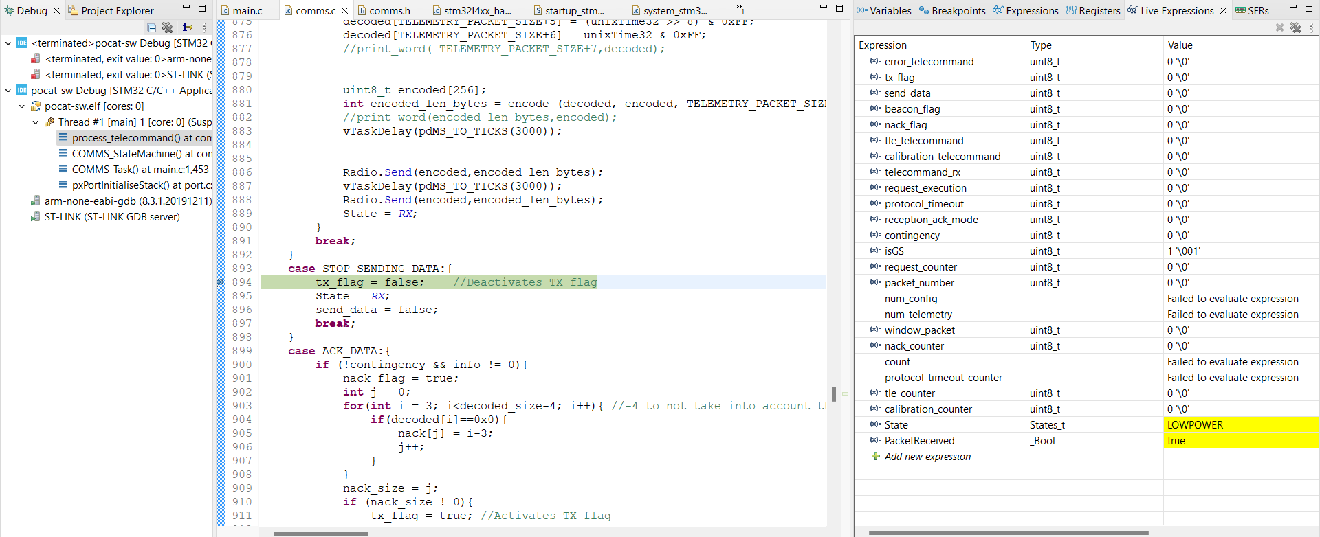
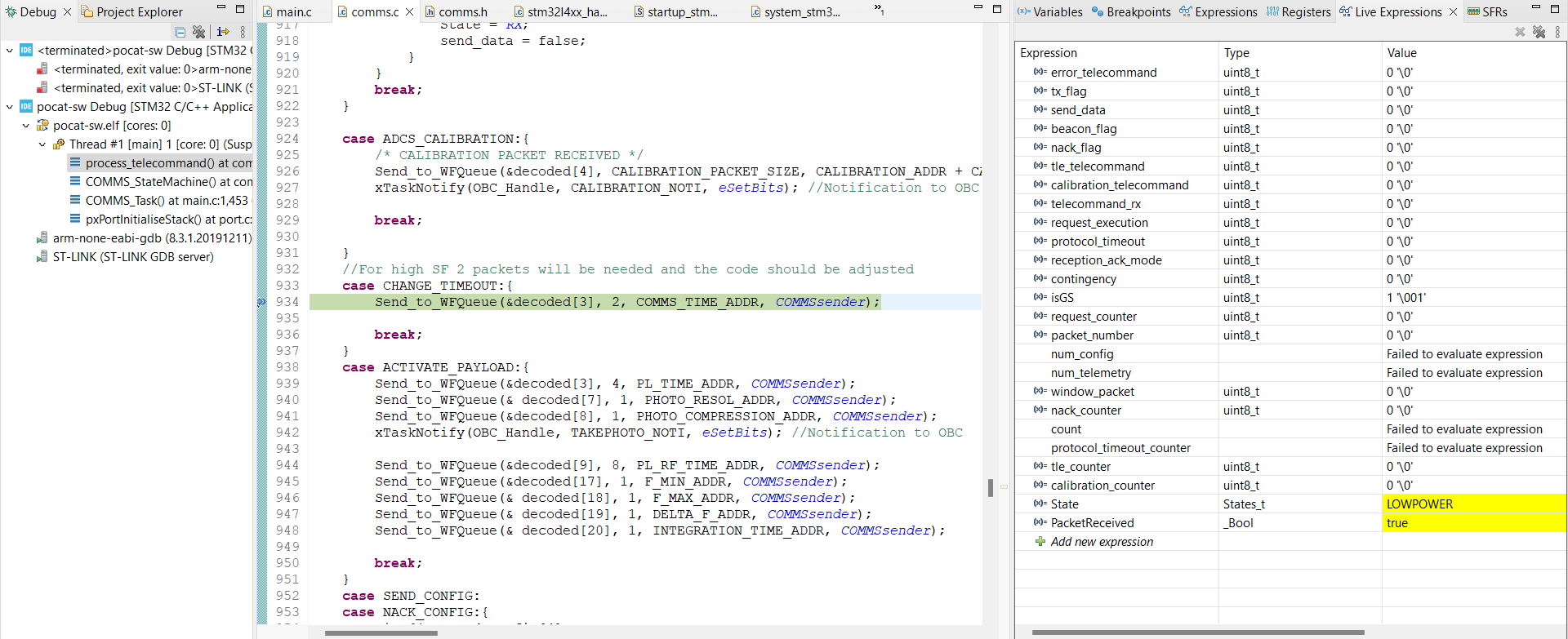
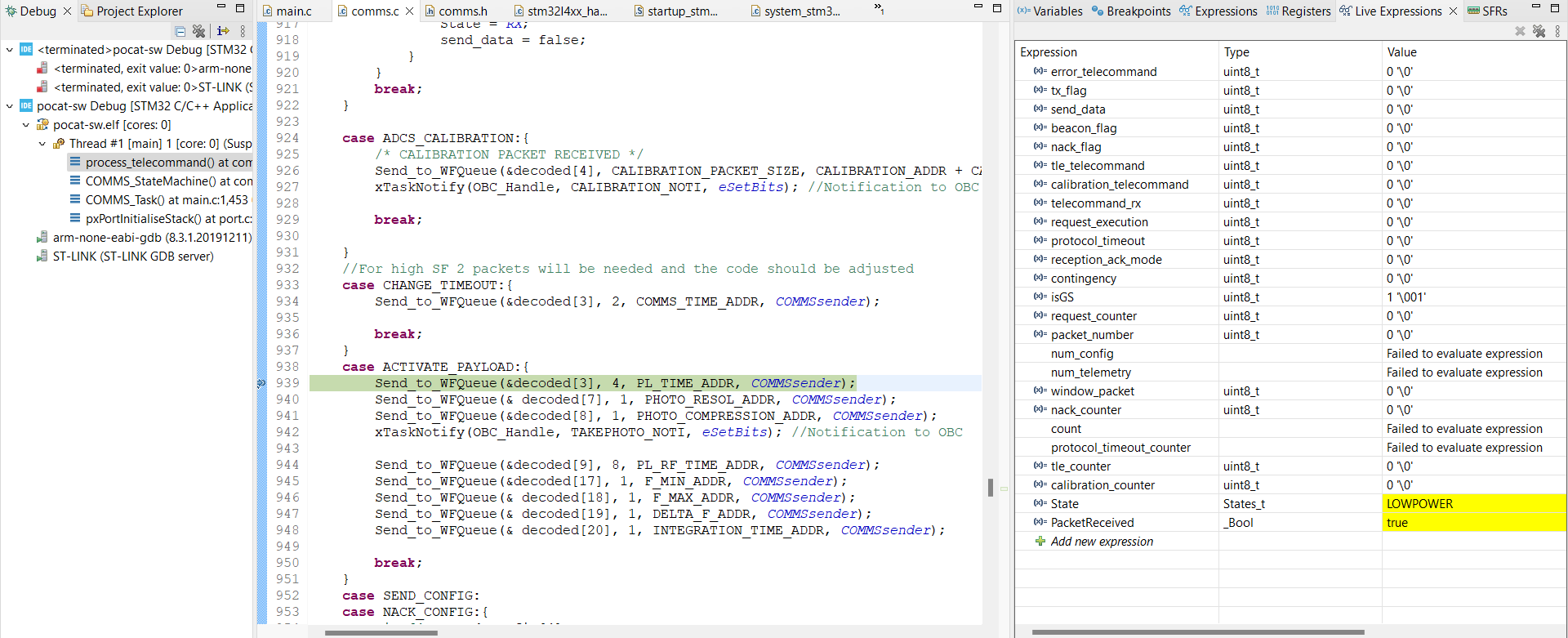
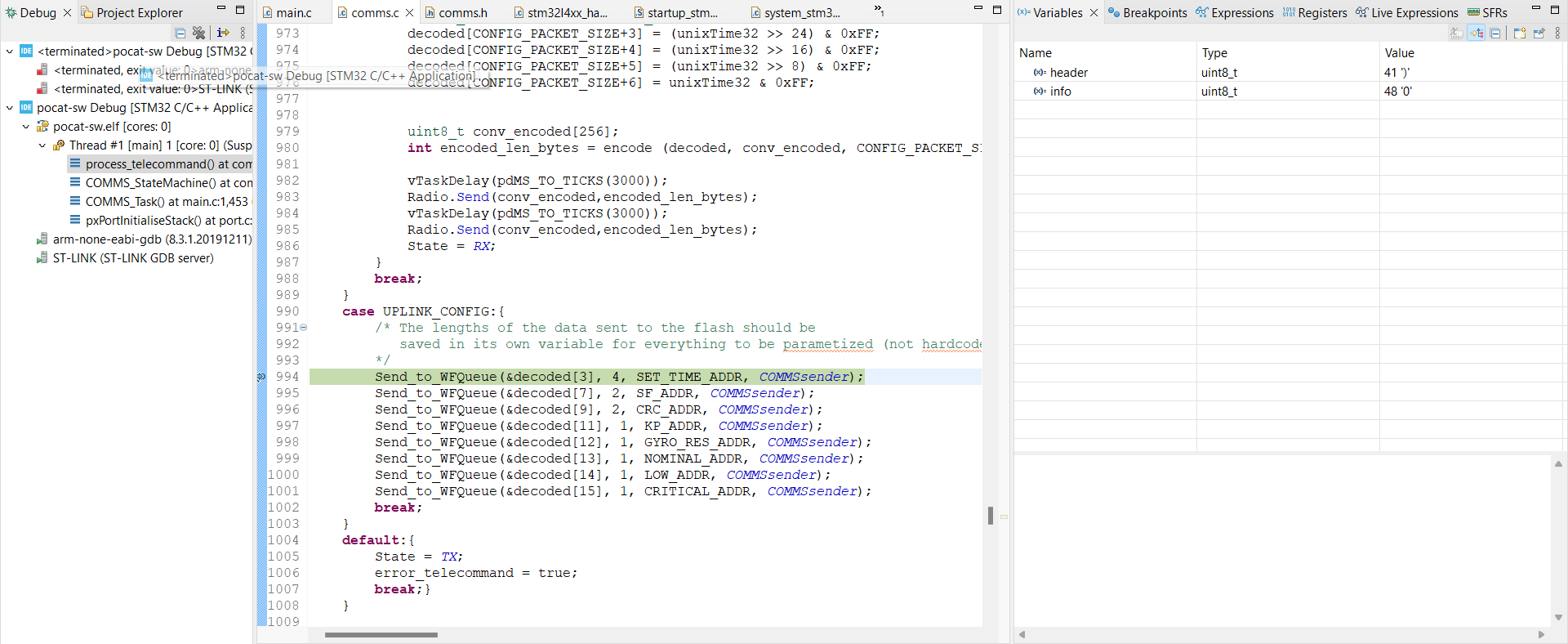
Upon flashing our code into the Nucleo and transmitting diverse telecommands with TinyGS, we discovered that the LoRa module failed to transmit responses to the telecommands as expected. Following a thorough and extensive investigation, we identified the root cause of the issue: during reception, the reception buffer requires slightly more time before decoding to effectively process the incoming packets. To address this issue, we implemented a solution by incorporating a small delay. Following this adjustment, we have successfully achieved the reception and response to telecommands sent by TinyGS, as demonstrated in here:
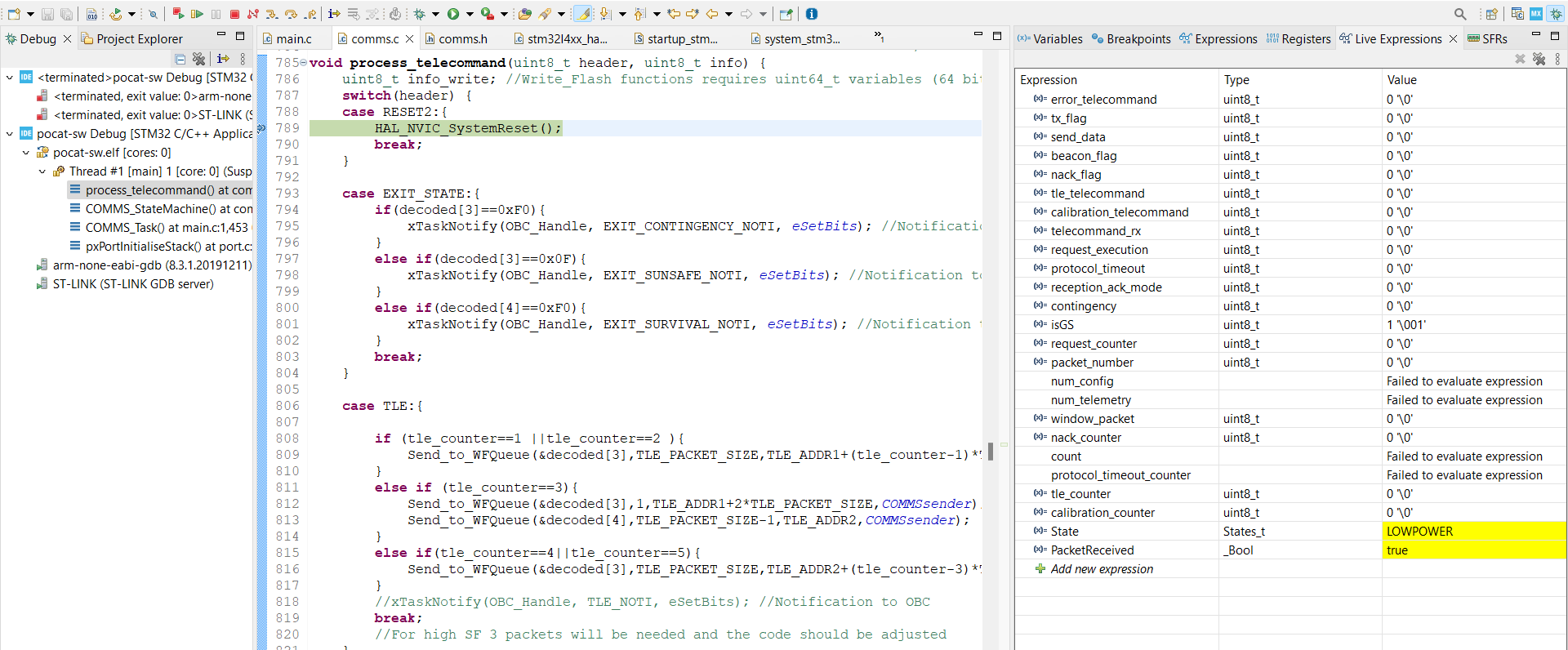
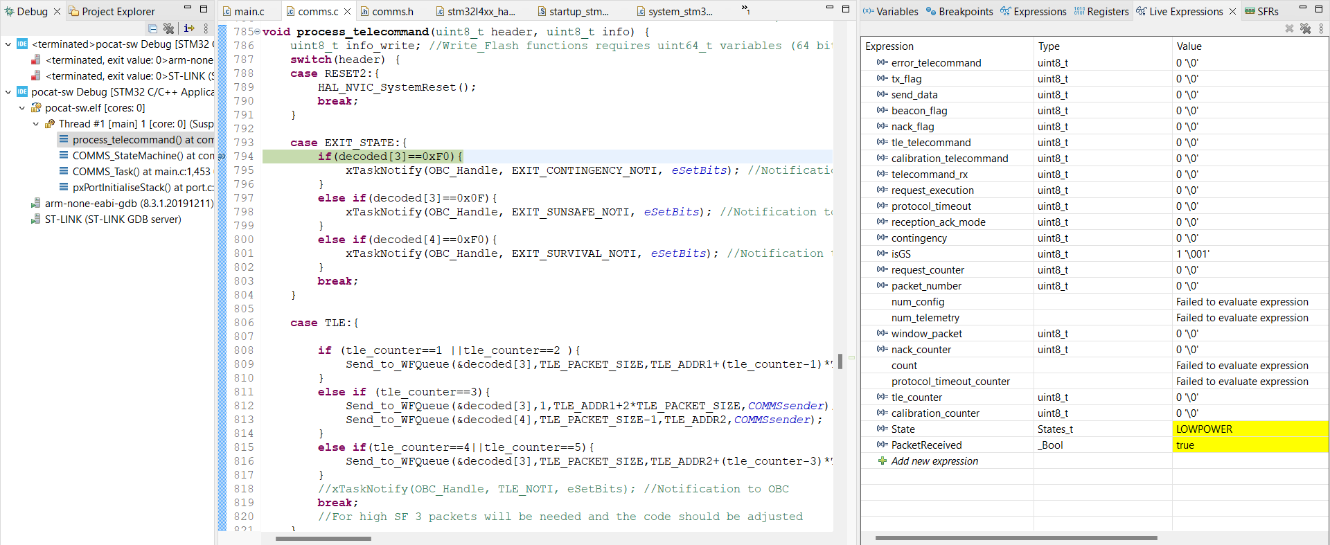
We will commence with telecommands that do not necessitate a response from the PocketQube. To verify proper functionality, we will insert breakpoints within each of these states for testing.
RESET
EXIT STATE
TLE
ADCS CALIBRATION
STOP SENDING DATA
CHANGE TIMEOUT
ACTIVATE PAYLOAD
UPLINK CONFIG
Subsequently, we will perform tests on all telecommands that necessitate a response from the satellite. To test these telecommands, we can choose to either insert breakpoints or examine the responses from the TinyGS terminal.
SEND DATA
SEND TELEMETRY
SEND CONFIG
We can affirm that all telecommands have been successfully transmitted by TinyGS, processed by the Nucleo+LoRa, and appropriately answered when required.
Step 4:
Following the success of the previous step, we proceeded to integrate the actual OBC-COMMS board. However, the experiment deviated from the plan due to several issues:
- The COMMS subsystem remained in LOWPOWER mode instead of transitioning to RX.
- The antenna seemingly received packets from unknown sources (likely interferences), leading to buffer overload.
- The subsystem failed to switch to TX when required.
While we initially anticipated hardware-related problems, a careful examination of variable values (such as the COMMS state or PacketReceived) suggests a potential issue with the OBC and task management rather than the hardware.
To address these issues, several actions were taken:
- COMMS Subsystem Stuck in LOWPOWER Mode: To tackle the problem of the COMMS subsystem not transitioning from LOWPOWER mode, we temporarily deactivated other tasks, as done in the previous step. This suggests a potential issue with the other tasks, likely originating from the OBC.
- Reception of Unknown Packets: To resolve the reception of multiple packets from unidentified sources, attempts were made to isolate the board and TinyGS in a homemade anechoic chamber. Despite these efforts, packets from unknown sources persisted. The next step involves replicating the experiment in a genuine anechoic chamber to determine if the issue can be resolved under controlled conditions.
- State Machine Not Transitioning to TX: Regarding the state machine's failure to transition to TX, it is believed to be a consequence of the previous issue. The satellite's inability to receive useful packets results in a fully occupied buffer, leading to the observed behavior.
UPDATE: Errors were detected on the OBC-COMMS board
1) Mirroring error in one of the OBC crystal oscillator:
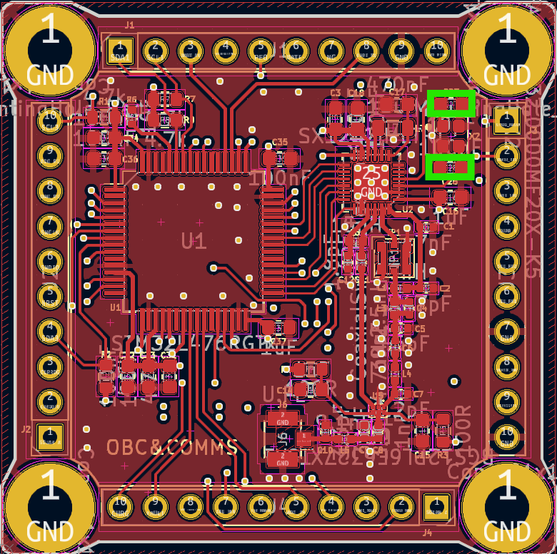
The error has already been corrected in the newest OBC-COMMS PCB design. The clock was removed from the board for this test as
2) Issue with the transceiver clock capacitors. Both transceiver crystal oscillators were removed as per the transceiver datasheet: "The SX1261/2 does not require the user to set external foot capacitors on the XTAL supplying the 32 MHz clock. Indeed, the device is fitted with internal programmable capacitors connected independently to the pins XTA and XTB of the device. Each capacitor can be set independently, balanced or unbalanced to each other, by 0.47 pF typical steps."
Both capacitors were removed.
After implementing the commented modifications to the board, the testing was resumed:
Step 5:
TBD.
Anomalies
As we've been reviewing the test results, several issues were encountered during the process:
During step 3, an issue arose during the reception process, which was successfully resolved by introducing a slight delay. The issue caused the system to "ignore" the sent telecommands.
In step 4, the COMMS subsystem persisted in LOWPOWER mode, necessitating the removal of tasks to facilitate the test. This indicates an ongoing challenge with the OBC subsystem task.
Another issue in step 4 involved the reception of numerous packets from unidentified sources. To address this, further solutions are needed, and the possibility of conducting tests within an anechoic chamber is being considered for better-controlled testing conditions
Conclusions
The issue pertaining to OBC task management must be tackled, as it seems to be the primary cause of the anomalies we discussed.
Furthermore, we must also tackle the problem of receiving numerous packets, as it hinders the reception of the genuinely important ones.
At the very least, we can affirm that the COMMS code is functioning correctly, and the OBC-COMMS board, equipped with the quarter-wavelength antenna, is capable of successfully receiving packets.
DYNEEMA TEST
Test description and objectives
This test aims to evaluate the chosen Dyneema for the antenna deployment. It involves measuring the time taken for the material to melt under atmospheric conditions.
Requirements Verification
- Dyneema must melt using 3.3V and 450mA in a timespan of 5-15 secs.
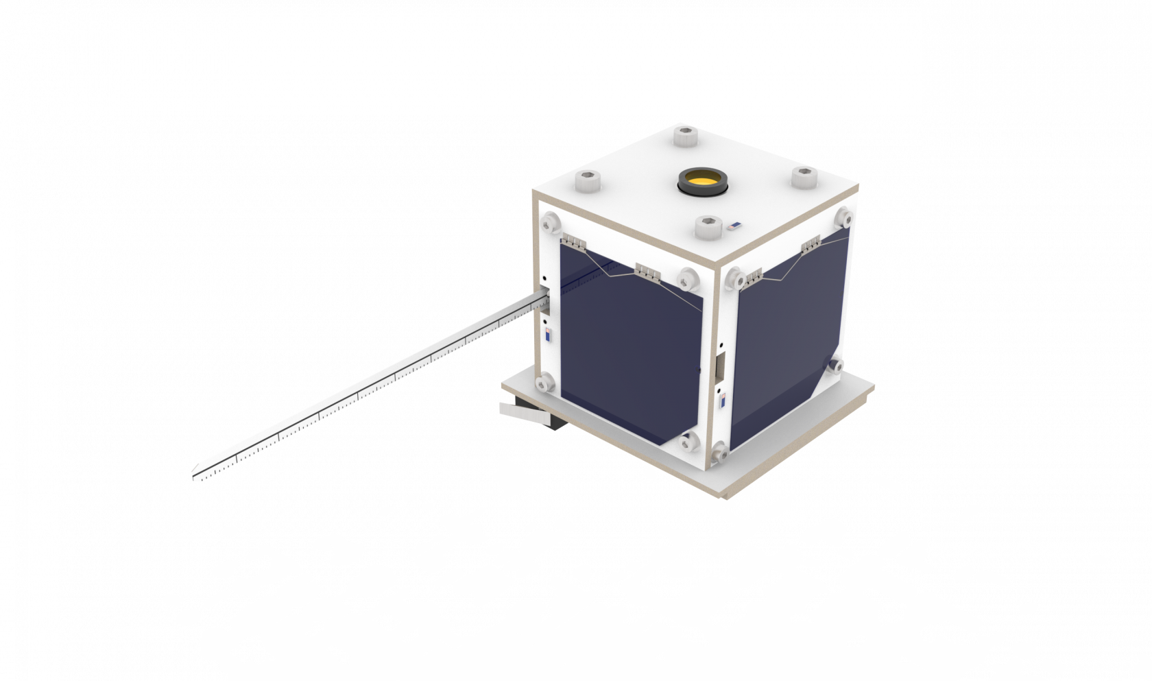
- Antenna must deploy correctly as shown in the render
Test Set-Up
Materials:
- Dyneema bought from Decathlon (UHMPE 0.35mm diameter, 26 kg)
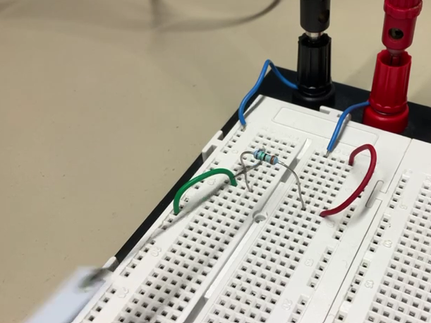
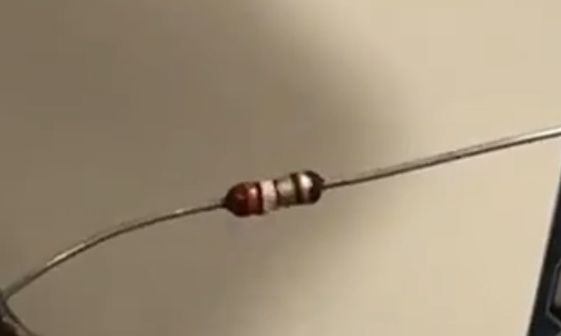
- 7.5 Ohm resistor (color code(5 bands): Violet, Green, Black, Silver, Brown)
- Voltage and current source
- Timer
Setup:
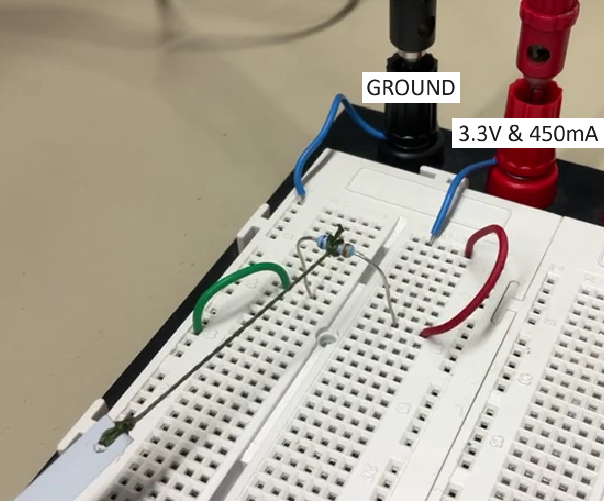
- Prepare the source at 3.3V and 450mA.
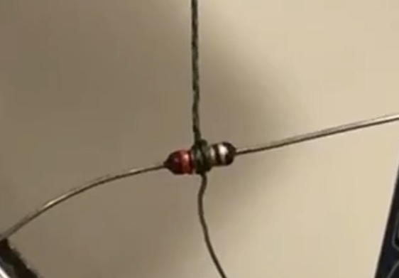
- Prepare a crossbow knot (explained in ᴾᵒCat Assembly and Integration >> Antenna >> Antenna Refurbishment) on the 7.5 Ohm resistor.
- Add a small weight in the other side of the rope to simulate the pressure experienced by the antenna when not deployed.
Pass/Fail Criteria
If Dyneema melts within the range of 10 to 15 seconds at 3.3V and 450mA, the test can be deemed successful. However, if it takes longer or fails to melt, the test will be considered unsuccessful.
Test plan
- Connect the resistor with the knot to the power source.
- Activate the power source and start the timer.
Test Results (1)
- t = 0s
The knot is connected to the resistor and the power source is connected. We used the weight of the lateral board with the antenna to simulate some pressure.
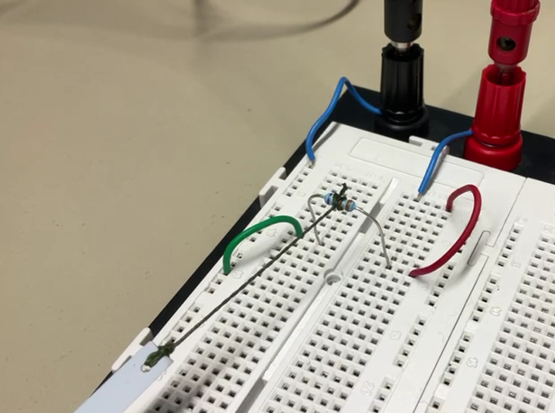
- t = 11s
The knot starts showing signs of degradation as the temperature of the resistor increases.
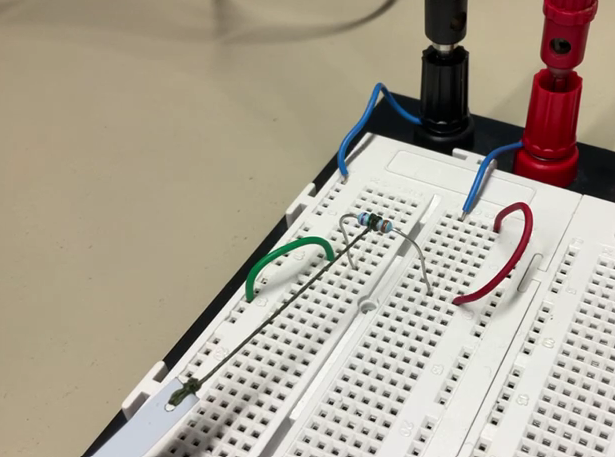
- t = 14s
The knot melts and the pressure provoques the antenna to deploy.
Some calculations:
Power (W) = Voltage (V) * Current (A) = 3.3 * 0.45 = 1.485 W
Energy consumed (J) = Power (W) * Time (s) = 1.485 * 14 = 20.79 J
Anomalies (1)
None. After repeating this test, it was determined that it needed to be redone as the dyneema did not burn, but melted instead.
Test Results (2)
- t = 0s
- t = 12s
Anomalies (2)
Possible problems with the EPS. Redo the test.
Conclusions
This experiment will undergo repetition within a vacuum chamber due to the differing thermal properties in such conditions. Dyneema is expected to exhibit a significantly faster melting rate as heat transfer with the absence of air in space is not a factor.
ANTENNA DEPLOYMENT TEST
Test Description and Objectives
The primary goal of this test is to validate the satellite's antenna deployment. This step is mission-critical as its proper function is pivotal for the transmission and reception of data by the satellite.
This test might (if possible) also test the comunications with the deployed antenna.
Requirements Verification
| Requirement ID | Description |
|---|---|
| ADTR - 01 | Dyneema must melt in less than 15 seconds in vacUum conditions. |
| ADTR - 02 | The antenna must deploy correctly, meaning that it should remain nearly completely straight after deployment. |
| ADTR - 03 | The spacecraft must be able to communicate with the ground station after antenna deployment |
Test Set-Up
Materials:
- PocketQube structure with the OBC-COMMS board and an EPS.
- Lateral board with an antenna and low impedance resistor (7.5 Ohms (color code(5 bands): Violet, Green, Black, Silver, Brown))
- Dyneema bought from Decathlon (UHMPE 0.35mm diameter, 26 kg)
- Computer
- Clean room for low contamination
- Vaccum chamber
- Clean room garment
Setup:
- Prepare the computer and a code to activate the "thermal knife" pin
- Refurbish the antenna as explained here
- Add the PocketQube in the vaccum chamber and prepare all connections
- Prepare vaccum (should take a time)
Pass/Fail Criteria
If the Dyneema melts in under 15 seconds in vacuum conditions and the antenna remains straight post-deployment, we will deem the antenna deployment test successful.
Test Plan
Step 1: Antenna deployment
Prior to conducting a test in the vacuum chamber, it is imperative to meticulously examine the feasibility of the test in atmospheric conditions. While the results may vary, the ultimate conclusion remains the same: if the dyneema melts in atmospheric conditions, it will likewise experience the same outcome in vacuum conditions.
To carry out this preliminary test, a PocketQube with, at a minimum, the OBC-COMMS and EPS subsystems is required. The EPS can be powered either by a direct power source or a battery. The activation of the thermal knife will be done using cables activating the BURNCOMMS pins from the OBC-COMMS board.
Step 2: Installation
The initial phase involves preparing the entire test setup, a critical step that will determine the feasibility of conducting the test under vacuum conditions. For this we will follow the Thermal Vacuum Chamber Operations Manual.
In our specific scenario, the test chamber will accommodate a PocketQube containing, at a minimum, the OBC-COMMS and EPS subsystems. The EPS will include a battery, serving as the power source for the thermal knife.
To activate the thermal knife, control over the OBC-COMMS board will be facilitated through cables.
Step 3: Antenna deployment in vaccum
After placing the PocketQube in vacuum conditions, we can initiate the antenna deployment test. To do this, we will activate the BURNCOMMS pin on the OBC-COMMS board. This pin is connected to a low-impedance resistor, which, in turn, is linked to the dyneema for the antenna deployment.
What we will do once we activate the pin is mesure the time it takes for the dyneema to test. We can later calculate the power consumed and perform adjustments if necessary.
Step 4: Transmission
This step is considered optional due to uncertainties regarding its feasibility in our small vacuum chamber. The objective is as follows: utilizing an additional antenna within the vacuum chamber, potentially a TinyGS, we aim to test the deployed antenna by establishing direct communication between the PocketQube and the auxiliary antenna, simulating a Ground Station. Attenuators may be employed to replicate challenging space conditions. The primary goal is to transmit telecommands and assess whether the satellite can respond as anticipated.

