Hardware Design
Design Choices
Up next is provided a table including the most important components of the EPS. In the following sections is found information about each one of them as well as the overall design of the system.
Quick Facts Table
| Component | Model |
|---|---|
| Solar Cell | Lightricity S3040_CIC |
| Battery | 3.7v 1400 mAh |
| MPPT | SPV1040TTR |
| Power Management | LTC4040 |
| Battery Sensor | DS2782E+ |
| Voltage Regulator | ISL9120IRTNZ |
| MOSFET | SIR424DP-T1-GE3 |
Table 1: EPS main components.
Solar Cells
The selected model is the S3040_CIC from Lightricity, a 30% Triple Junction Gallium Arsenide and Ultra High-Efficiency solar cell. Note that due to a recent shortage of supplies from the solar cell provider, it was necessary to seek alternatives and switch to a new provider and model. Consequently, certain values, parameters, and renders are still being defined and are in the process of being updated. The cells were chosen due to their availability as well as their capability to meet al requirements established.
Figure 1: Lightricity S3040CIC (Solar array)
The following tables show the main specifications of S3040_CIC solar arrays and their physical dimensions:
| Lightricity S3040CIC | |
|---|---|
| Integration | CIC (Coverglass Interconnected Cells) |
| Size (mm) | 40.15 × 30.35 × 0.30 |
| PV active area | 12cm² |
| Voltage output (AM0) | ~ 2.5V |
| Power Output (AM0) | ~ 0.5W |
Table 2: Solar array main specifications.
Note that the array has Coverglass Interconnected Cells (CIC), a specific type of solar cell assembly used in space-grade solar panels. The term refers to a system in which individual solar cells are interconnected and covered with a thin protective glass layer.
Also notice that both voltage output and power output is presented at AM0, which indicates the measures are given at Air Mass Zero, outside the Earth's atmosphere, therefore without it's filtering.
PV active area indicates the area of the array in which the photovoltaic efect is produced.
The solar array dimensions and physical properties are provided in Table 3:
| Dimensions | |
|---|---|
| Max. length L (mm) | 40.15 |
| Max. width W (mm) | 30.35 |
| Total thickness (µm) | 300 |
| Coverglass thickness (µm) | 100 |
| Interconnector (Ag) thickness (µm) | 25 |
| Total cell area (cm²) | 12 |
| Total weight (mg/cm²) | <120 |
Table 3: Solar array dimensions
In the next tables the electrical parameters are presented, both at the Beginning of Life (BOL) and at End of Life (EOL). Then an explanation is given of each one.
| Main electrical parameters | BOL | EOL (10^15 e.cm^-2) |
|---|---|---|
| Voc (V) | 2.74 | 2.48 |
| Jsc (mA.cm^-2) | 17.2 | 16.7 |
| Vmp (V) | 2.45 | 2.26 |
| Jmp (mA.cm^-2) | 16.4 | 15.4 |
| Efficiency (%) | >30.0 | 25.7 |
Table 4: Solar cells main electrical parameters
| Thermal coefficients | BOL | EOL (10^15 e.cm^-2) |
|---|---|---|
| dVoc / dT (mV.°C^-1) | -5.9 | -6.2 |
| dJsc / dT (µA.cm^-2.°C^-1) | 14.8 | 14.6 |
| dVmp / dT (mV.°C^-1) | -6.5 | -6.9 |
| dJmp / dT (µA.cm^-2.°C^-1) | 9.9 | 10.1 |
Table 5: Solar cells thermal coeficients
Voc (Open-circuit voltage) indicates the maximum voltage produced by the cell when exposed to sunlight but not connected to a load, this parameter presents a variation of around -6 mV for each increase of a temperature degree. Jsc (Short-circuit current density) corresponds to the maximum current density produced by the cell when shortcurcuited, with a variation of around -15 µA/cm^2 for each degree incease.
Vmp and Jmp indicate the maximum value of these parameters when power is at its maximum. Both have a variation of the same order as the aforementioned corresponding ones.
Lateral & Bottom Boards
The lateral boards have an area of 23 cm^2, while the solar cells have an active area of 12 cm^2. Thus, 52% of the lateral board area is occupied by the solar cells. Regarding the bottom PCB, its area is 33.3 cm^2, and the solar cells occupy 36% of this area. The payload section has a surface area of approximately 20.1 cm^2, but it does not contain any solar cells.
In conclusion, solar cells cover 41% of the total exterior surface area of the PocketQube. Each solar cell 3.52 has four pins: two on the top, one in the corner, and the last one on the entire backside. When mounted on the lateral board, the solar cell will be soldered by its back pin and the three top pins. The attachment of the solar cells to the PCB will rely on these solder joints, especially as the backside of the solar cell is a large pad, providing sufficient soldering area to secure the cell properly.
Figure 2: Image of the solar cell pins
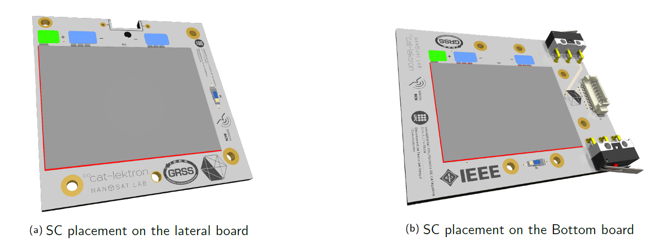
Each lateral board and bottom board has one solar cell each. The cells are soldered to the PCBs in such a way that they remain securely attached without the need for adhesives or additional supports. In the following Figures 3 and 4, we can see that there are four soldering pads: two blue pads representing the negative pads, and the red pad covering the entire back of the solar cell, which corresponded to the positive pad. Additionally, the green pad located in the upper left corner is associated with the By-Pass diode.
Figure 3: Solar Cells Placement
The By-Pass diode in solar cells is essential for series connections, ensuring that if one cell fails, the others remain unaffected. However, in our spacecraft, parallel connections are used, making the By-Pass diode unnecessary. If required, connecting the negative pad to the diode pad would suffice, as shown in Figure 4.
Figure 4: Solar Cell By-Pass diode placement and connection
Battery
When selecting a battery for the satelite, it is essential to choose one with the highest possible capacity that can still fit within the space constraints.
The battery selected is a 3.7 V 1400 mAh LiPo battery, with a size of 42 x 35 x 10 mm and a weight of 23.4g , and was chosen for the following reasons:
- Energy Efficiency: The battery operates between 3.7V and 4.2V. Since the system runs at 3.3V, reducing the voltage to 3.3V is more efficient than stepping it up.
- Temperature Tolerance: LiPo batteries can handle extreme temperature fluctuations, which is crucial for space environments. However, charging is restricted to temperatures above 0 ◦C, and operation is limited to certain ranges. If not regulated, improper temperatures can lead to battery failure. However, the EPS’s integrated circuit will help manage this to prevent potential failures.
- PocketQube Compliance: The selected battery adheres to the PocketQube standard in terms of both size and weight, making it an ideal option.
- Depth of Discharge: For a mission lifespan of 2.7 years (approximately 15,100 cycles, given a 94-minute orbital period), the battery’s discharge rate per cycle is a key factor. Ensuring proper discharge control is crucial for longevity.
In the next table the electrical parameters of the battery are presented:
| Parameters | Value |
|---|---|
| Part Number | LP 103438 |
| Nominal Voltage | 3.7V |
| Nominal Capacity | 1400mAh |
| Internal Impedance | <60mΩ |
| Charge Voltage | 4.2V |
| Recommended Charge Current | 0.2C |
| Allowed Max Charge Current | 0.5C |
| Output Voltage Range | 2.5V - 4.2V |
| Recommend Discharge Current | 0.2C |
| Max Continuous Discharge Current | 1C |
| Pulse Discharge Current | 3C (10ms) |
| Discharge Cut-off Voltage | 2.5 ± 0.05V |
| Cycle Life to 80% Health | 500 (0.2C, 25 °C) |
Table 6: Battery electrical parameters
The battery will be enclosed within a PTFE structure, ensuring it is well-secured and protected from potential impacts during satellite operation. The enclosure is designed not only to secure the battery but also to minimize the risk of fragment release in the event of a battery explosion. It provides a containment barrier, preventing fragments from escaping and damaging other satellite components.
Figure 5: Battery PTFE structure
Also in case the battery swells due to overheating, this structure allows for slight expansion while preventing excessive swelling.
The battery also includes several features designed to prevent damage to both the battery, and to the satellite. It incorporates an IC (G3R) and a MOSFET (CJ8810) on an internal board, which provide this protection. If the voltage drops to 3.0 V, the battery will automatically disconnect protecting against overdischarge. Similarly, if the charging voltage reaches 4.28 V, it will automatically disconnect to protect against overcharging. Additionally, thanks to these components, it also offers protection against short circuits and overcurrents by temporarily cutting off the output, preventing damage to both the battery, and to the satellite
MPPT
The MPPTs are responsible for maximizing the power generated by the solar cells. The STMicroelectronics SPV1040 was chosen due to it being able supports a parallel connection between the multiple solar array axes and having great efficiency. Another reason was because the manufacturer also provides simulation tools (eDesignSuite) that can be used for both dimensioning the biasing elements, as well as obtaining characteristics describing the current application. This greatly simplifies the development process and avoids potential design incompatibilities or errors.
The SPV1040 has an efficiency of up to 95% which minimizes energy losses from the solar cells, providing an output from the Energy Harvest Block between 0.3 and 5.5 V. This is critical due to the present power constraints.
Further information on the MPPT's can be found in their correspondant datasheet:
Power Management IC
The power management IC chosen was the Analog Devices LTC4040. This component was chosen because it offers control over the battery operation and is interfaceable with the On-Board Computer through basic logic pins. Moreover, the chip also offers a few safety features, in order to prevent damage that can be inflicted by over-currents, over-voltages and temperatures exceeding our established limits.
Some other notable feautures that made the decision clear are:
- Automatic switch from the solar power operation to battery operation, with the option of manual operation
- Battery-only power-up of the chip
- NTC Battery temperature monitoring and operation control
- Adjustable output current limiter
- Adjustable charging current (depending on the output current demand)
- Buck regulator for the battery charger
- Boost regulator for the battery discharger
- Faults and status output flags
Battery Sensor
The battery sensor chosen is the Analog Devices DS2782E+ it was selected due to its capacity to measure voltage, temperature and current, and estimate available capacity for rechargeable lithium-ion polymer batteries.
EPS Voltage Regulator
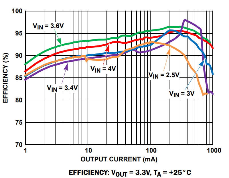
The voltage regulator chosen is the ISL9120IRTNZ, with up to 98% efficiency, it provides a constant output voltage of 3.3 V with a maximum current of 800mA. Since the battery produces between 3.7 V and 4.2 V, the regulator will reduce the voltage to 3.3 V, which is more energy-efficient than increasing the voltage.
A factor in the decision of selecting this part was the efficiency of the devide under the current conditions requiered by the PocketQube. The next figure ilustrates the effecinecy dependancy on consumption:
Figure 6: Voltage regulator efficiency
This regulator is also designed to prevent errors in any subsystem from impacting the battery and vice versa. It includes features such as over-temperature protection and undervoltage lockout. The over-temperature protection mechanism disables the device if the chip temperature exceeds 150°C, automatically reactivating it once the temperature falls to 115°C. Meanwhile, the undervoltage lockout function prevents the regulator from operating when the input voltage is too low, thereby ensuring the system functions correctly and safeguarding both the circuit and the battery.
Umbilical Voltage Regulator
The umbilical connector allows for battery charging, ans so this process is to be controlled and regulated by Texas Instruments TPS7A7002 a high-performance, positivevoltage, low-dropout (LDO) regulator. The devide was chosen due to its featuring of ultra-low dropout, useful as the input voltage through the connector is close to the charging voltage of the battery.
Schematic Design
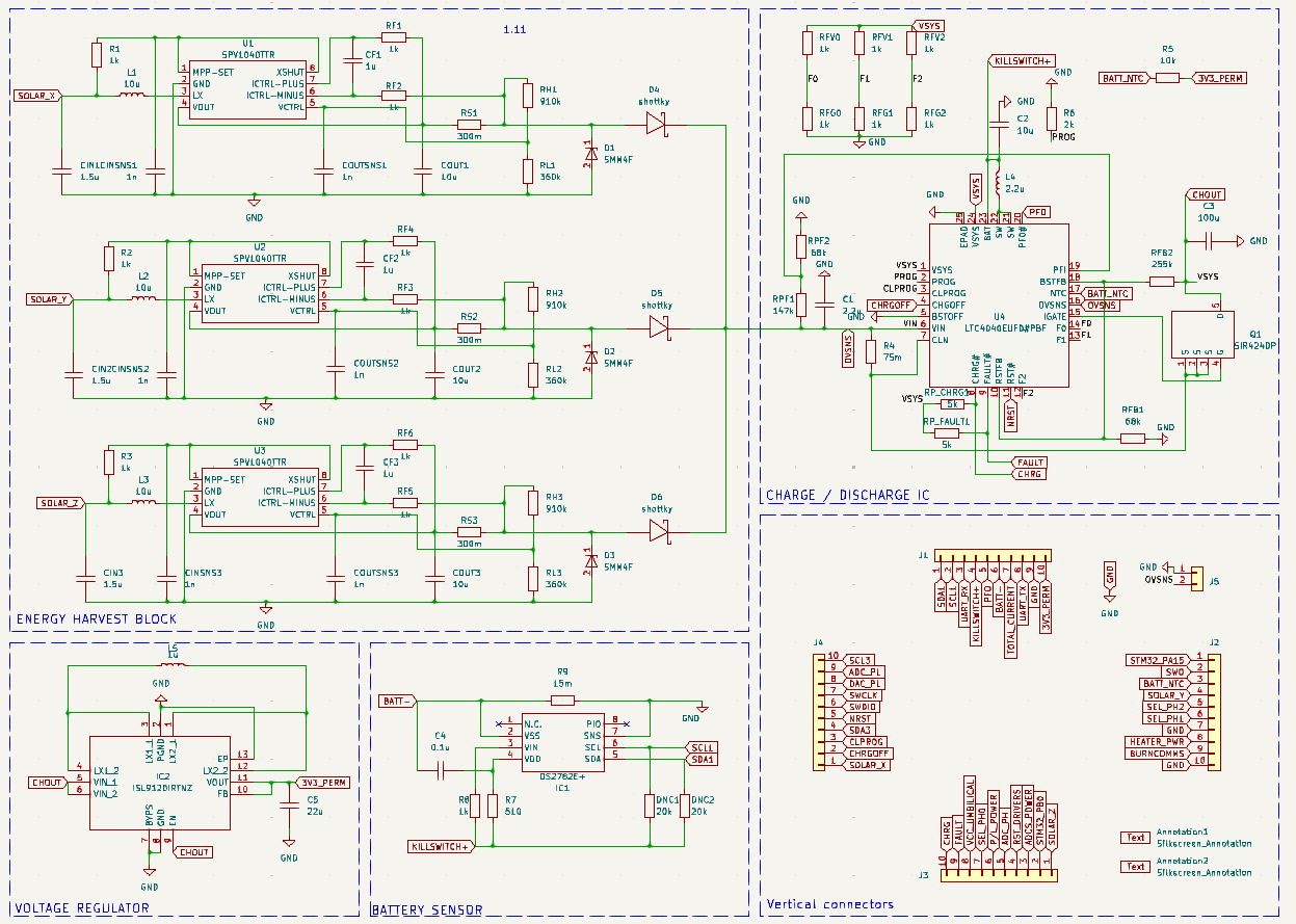
The hardware schematic represents the subsystem connections between components as well as all the inputs and outputs in a clear, easy to work with, manner. This section will begin with the schematic of the different blocks and components of the EPS, ending with a general view of the whole design.
Energy Harvest Block
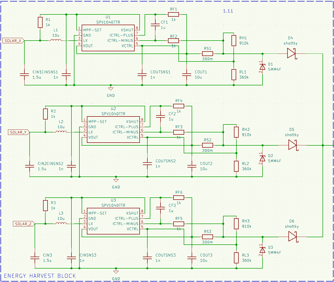
The energy harvest block main compontents are the solar cells as well as the MPPTs, providing an efficient power generation block, and, to ensure the integrity and safety of these components, a Schottky diode, avoid potential power returns to the block. The MPPT connections and components schematic was generated by eDesignSuite. The next figure is the block schematic:
Figure 7: Energy Harvest Block Schematic.
Note that there is a difference bewtween the generated design and the one used. This is the change of the 6x4.7uF capacitors at the input of the MPPTs in exchange for a single 1.5uF. Observe that the only inputs are the solar panels powers and the output is the regulated voltage at around 4.4V (the battery charges at 4.2V).
Power Management IC **
The charging/discharging operations of the battery are managed and performed by the power management IC, the central piece of this subsystem block. To understand the schematic it is convenient to have clear how the main IC works:
If there is a high enough voltage (programmable) at its input, then it will output the input, while charging the battery from the same power. As the current demand on the load increases, the chip automatically decreases the battery charging current. The battery is charged through a buck regulator to step down the voltage to the selected battery charging voltage. The charging voltage can be selected using the F0,F1 and F2 pins as such:
Table 7: PM IC Control Voltages
As the satellite enters the eclipse and the voltage output by the MPPTs decreases, the chip will automatically switch to discharging the battery.
The design followed corresponds to the reference application provided by the manufacturer but set up for our necessities. The schematic is presented in the next figure and then explained: 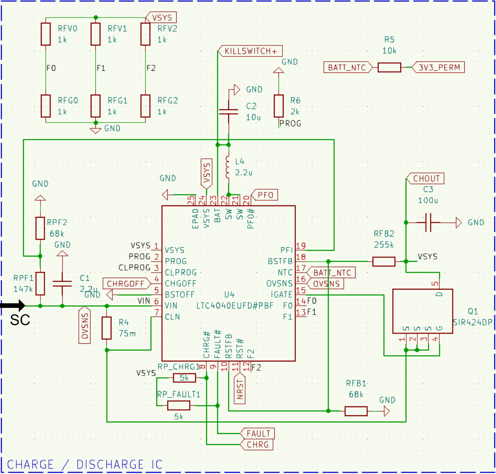
Voltage Regulator
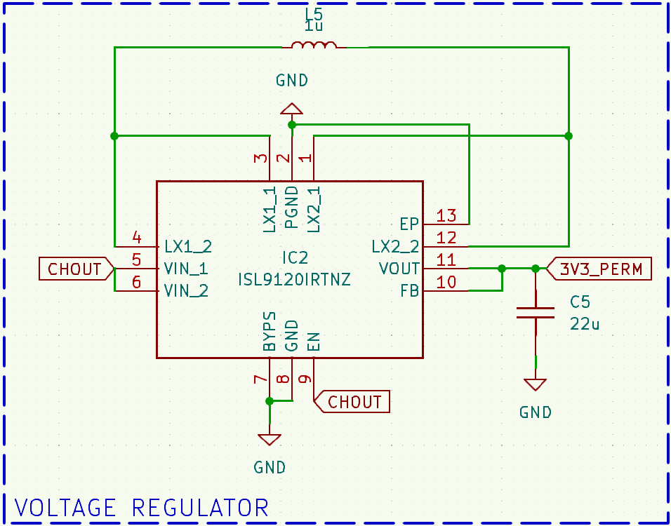
The voltage regulator is a buck-boost switching regulator that, in our case, will take as an input a voltage higher than the one it supplies as an output. The design chosen coincides with the typical design provided by the manufacturer, with the bypass mode deactivated, leaving the buck-boost mode on.
Figure 9: Voltage Regulator schematic
Battery Sensor
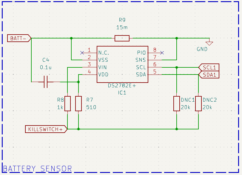
The battery sensor communicates through I2C with the OBC (SCL1,SDA1). It takes as inputs the battery poles and provides measures of it's temperatura, voltage, current and an estimation of capacity. The schematic is provided up next, guided by the manufacturers instructions:
Figure 10: Battery Sensor Schematic
Solar Cell Connections
The Solar Cells are located in the outer boards and interface with the lateral Picoblade connector:
Figure 11: Solar Cell Outer Board Connections Schematic.
Note that this circuit is located in the outer boards.
Killswitches
The killswitches remain pressed when inside the deployer and are only released when the PocketQube is ejected. While only one would be necessary two are chosen for redundancy and symmetry. They are connected to the positive pole of the battery and ensure no power is provided by it when pressed.
The schematic is provided next:
Figure 12: Killswitches Schematic.
Note that this circuit is located in the bottom board.
Charging Protections (Umbilical Voltage Regulator)
The umbilical connector allows for battery charging. This proccess is regulated and protected by the TPS7A7002, and the schematic follows the usual design presented by the manudacturer. It takes as an input the charging power from the connector and yields power to the battery as its only output.
The schematic is provided next:
Figure 13: Umbilical Charge Voltage Regulator Schematic.
Note that this circuit is located in the bottom board.
EPS Schematic Overview
Figure 11: EPS PCB Schematic Overview
PCB Design
EPS Board
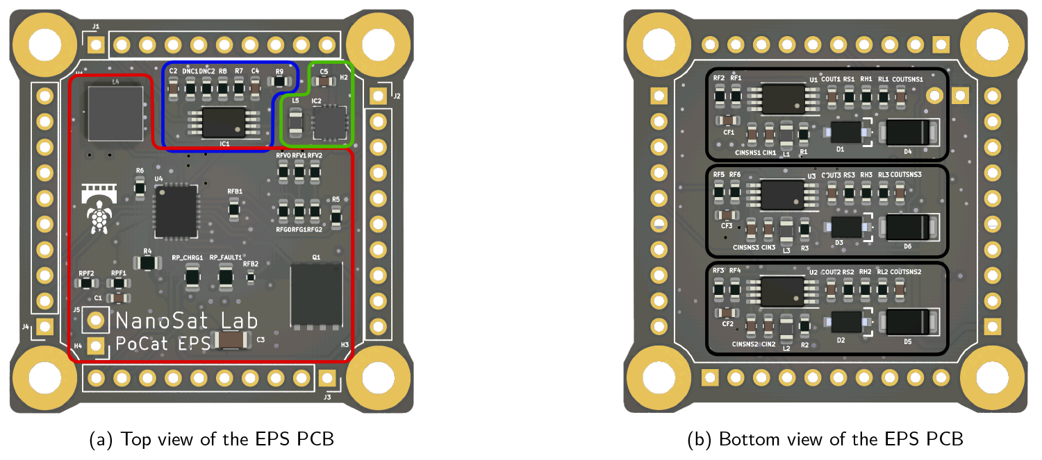
The EPS PCB is structured so that the different blocks are easily identifiable and accessible for maintenance. If we take a look at the PCB, we can see that the back Figure 12 is dedicated to the Energy Harvest Block, which contains only the MPPTs. Here, we can observe that all three MPPTs are connected in parallel, and despite they being identical, it should be easy to identify possible errors during testing. On the front Figure 12, the rest of the components are located. We can see that the part related to the Power Management IC is highlighted in red, the in battery monitor IC in blue , and the Voltage Regulator in green.
Figure 12: Views of the EPS PCB
The Energy Harvest Block is placed on the bottom layer of the PCB. Three identical blocks are placed in parallel receiving the power from the X (2 cells array), Y (2 cells array) and Z (single cell array) solar cells through the vertical connectors. The design tries to maximize compactness and cleanness in order to facilitate testing while making sure a failure in a single solar array does not become critical to the power integrity of the system.
The Power Management IC block has the main IC (LTC4040EUFD#PBF) centered on the top layer of the PCB in order to minimize the distance between the IC and the components it controls, reducing power path resistance and minimizing voltage drops. Placing the IC in the middle also helps with thermal distribution as significant heat is generated through its operation. The rest of the deisng follows standard practices to minime voltage spikes, such as the placement of decoupling capacitors to ground and so on.
The battery monitor IC and the Voltage Regulator are located as close as possible to the vertical connectors and the corner of the PCB. As the voltage regulator can generate significant heat this desicion is intended to help heat dissipation by providing more cooling space. This placement also intends to reduce thermal interference to the power management IC.
Being close to the connectors means being close to entry points of the PCB, avoiding the issues of measuring after distribution in case of the battery monitor, and the issues of power distribution for the voltage regulator.
PCB Layers
The EPS PCB is comprised of the following layers:
Figure 13: EPS PCB Layers


