# ᴾᵒCat: VGA Payload
# Subsystem Description
## Document scope
This document aims to give insight into the design choices taken in the development of the P/L 1, a video graphics array camera (VGA) conceived originally to monitor the deforestation of the Indonesian rainforest, but later repurposed to collect data of ice levels in polar regions as well as take pictures during the deployment of other artificial satellites.
## Camera selection and requirements
### Camera selection
Aligned with the original goal of this payload the camera selected was one which could, first of all, be interfaced with the OBC and offered a resolution higher than 640x480 pixels. Therefore an array of cameras were considered:
| NAME | RESOLUTION >= 640x480 | INTERFACE | CHANGEABLE FOV |
|---|
| GalaxyCore GC0308 | Y | USB 2.0 | Y |
| CMT-0.3MP-MK0806-R016 | Y | USB 2.0 | N |
| SC13MPA | Y | TTL, RS232, RS485 | N |
| SC03MPA (VGA) | Y | TTL, RS232, RS485 | Y |
| PTC06 | Y | TTL, UART | Y\* |
| SCB-1 | Y | TTL, RS232 | N |
Table 1: Camera comparison.
\*Through manual adjustment Highlighted in blue, the selected camera was the PTC06 manufactured by Putai Electronic Technology, Ltd., as it could be interfaced with the OBC, offered the aforementioned resolution and, as a differential factor, it provided serial JPEG compression and data transmission. The datasheet of the PTC06 is provided [here](https://www.mouser.com/datasheet/2/737/adafruit_english%20camera-1217461.pdf), and further information provided by the manufacturer can be found [here.](https://www.putal.com.cn/556/617/32) A rudimental translation can be downloaded here [Translated PTC06](https://wiki.nanosatlab.space/attachments/413). Some relevant specifications are provided in the following table:
| **SPECIFICATION** | **VALUE** |
|---|
| Size | The camera module size is 20x28x9 (not counting the connector height) mm. |
| Resolution (pixels) | VGA (640x480), QVGA (320x240), QQVGA (160x120) but we will preferably use the VGA. |
| FOV Diagonal | 64° |
| Distortion | 0.38% |
| Relative illumination | >53% |
| Operating conditions | The camera will work in the range of -20°C to 85°C. |
| Weight | 3g |
| Operating voltage | The camera can work from 3.3V to 5V. |
| Current consumption | The operation current will be 100mA. |
| Data format | JPEG, stored as an array of HEX bytes. |
Table 2: PTC06 Main Specifications
### Requierements
A list of high-level requirements was elaborated so as to determinate clear guidelines within which the camera payload must operate in order to achieve reliable and quality performance.
- S-CAM-0010: Interface with OBC.
- S-CAM-0020: Minimum #pixels (640 x 480).
- S-CAM-0030: Changeable FOV\*.
- S-CAM-0040: Lens made of glass.
- S-CAM-0050: Temperature range -20 to +60 °C.
- S-CAM-0060: SNR of the images larger than 45dB.
- S-CAM-0070: The resolution should be good enough to notice 100m differences.
- S-CAM-0080: Camera works with 3V3.
- M-CAM-0010: Robustness of the camera in the PCB.
- M-CAM-0020: SNR images larger than 45 dB.
- M-DATA-0010: Acquire 2 images per day.
Due to the selection of the PTC06 some criteria are already successfully meet. The following table provides more insight into the matter:
| **REQUIREMENT** | **STATUS** |
|---|
| S-CAM-0010 | Successfully interfaced through UART |
| S-CAM-0020 | Implemented, further testing required |
| S-CAM-0030\*\* | Small change is achieved, but causes bad focalization, further testing required\*\* |
| S-CAM-0040 | Met |
| S-CAM-0050 | Met, environmental testing required |
| S-CAM-0060 | - |
| S-CAM-0070 | Not meetable |
| S-CAM-0080 | Yes |
| M-CAM-0010 | - |
| M-CAM-0020 | Met |
| M-DATA-0010 | Many more can be acquired although not sent due to the data budget bottleneck |
Table 3: Camera Requirements Status
## Communications protocol
The communication protocol used to transfer data between the camera module and the OBC is UART *(Universal Asynchronous Receiver-Transmitter).* In concordance with its name, there is no clock usage on the protocol, which means that the communication is simplified as a Serial Communication Scheme. A serial communication consists of transmitting all the information only using two cables, RX-TX and TX-RX.
In general, the main characteristics of UART protocol are:
- Due to its simplified structure, it can be easily implemented.
- The protocol does not depend on any clock.
- The protocol uses only two wires.
- As with any serial communication, the information is transmitted between the TX-Transmitter pin to the RX-Receiver pin and vice versa.
#### Interface
The transmitting UART is connected to a controlling data bus that sends data in a parallel form. From this, the data will now be transmitted on the transmission line (wire) serially, bit by bit, to the receiving UART. This, in turn, will convert the serial data into parallel for the receiving device.
The UART lines serve as the communication medium to transmit and receive one data to another. Take note that a UART device has a transmit and receive pin dedicated for either transmitting or receiving.
For UART and most serial communications, the baud rate needs to be set the same on both the transmitting and receiving device. The baud rate is the rate at which information is transferred to a communication channel. In the serial port context, the set baud rate will serve as the maximum number of bits per second to be transferred. The used baud rate in our communications is of 11520 bps.
[](https://wiki.nanosatlab.space/uploads/images/gallery/2024-03/ZqOuart.png)
#### Data transmission
In UART, the mode of transmission is in the form of a packet. The piece that connects the transmitter and receiver includes the creation of serial packets and controls those physical hardware lines. A packet consists of a start bit, data frame, a parity bit, and stop bits.
Our data frame will be of 8 bits, and it'll include a parity bit in order to ensure more reliable communications.
More information about the UART protocol can be found here: [UART.](https://wiki.nanosatlab.space/attachments/412)
## System Description
The OBC is the main transmitter who sends the information from the STM32 to the camera, and the camera responds to this information. The camera is expected to receive a command and will act depending on the command it receives. The camera has different functions:
- Capture image.
- Read image data length.
- Read image data.
- Stop capture.
- Setting image compressibility.
- Setting image resolution.
The commands are different for each function. Here is an example of a communication between the OBC and the camera with the function “Reset”. The OBC sends a command to the camera saying that it wants to use this function, the command that will be sent is: 0x56 0x00 0x26 0x00. If the communication is correct and the camera has received the command properly, it will send another command to answer the OBC that he has done it, and to make sure that it has worked. The command that the camera will send the OBC is: 0x76 0x00 0x26 0x00.
#### Command Protocol (Hex format data)
For each function there are different commands, so in order to understand which is needed to be sent and to be received, a summary is presented in the following table.
| **FUNCTION** | **TRANSMITTED COMMAND** | **RECEIVER TRANSMITTED COMMAND** |
|---|
| Reset | 0x56 0x00 0x26 0x00 | 0x76 0x00 0x26 0x00 |
| Set image compressibility | 0x56 0x00 0x31 0x05 0x01 0x01 0x12 0x04 0xXX (\*) | 0x76 0x00 0x31 0x00 0x00 |
| Set image resolution | 0x56 0x00 0x31 0x05 0x04 0x01 0x00 0x19 0xXX (\*\*) | 0x76 0x00 0x31 0x00 0x00 |
| Capture an image | 0x56 0x00 0x36 0x01 0x00 | 0x76 0x00 0x36 0x00 |
| Read image data length | 0x56 0x00 0x34 0x01 0x00 | 0x76 0x00 0x34 0x00 0x04 0x00 0xXX 0xYY |
| Read image data | 0x56 0x00 0x32 ... 0x0A | 0x76 0x00 0x32 ... 0x00 |
| Stop capture/Clear image cache | 0x56 0x00 0x36 0x01 0x03 | 0x76 0x00 0x36 0x00 0x00 |
Table 4: Command Protocol
(\*) The 0xXX is the value of compression that will be set to the image. The range of values that are available are from 0x60 to 0XFF. The 0x60 refers to the minimum compression, and the 0xFF to the maximum compression.
(\*\*) The 0xXX is the value of resolution that will be set to image. This variable can only take three values: 0X00, 0x11 and 0x22, where 0x00 refers to the highest resolution (VGA) of 640x480p, 0x11 offers a QVGA resolution of 320x240p and 0x22 the minimum possible resolution (QQVGA) of only 160x120p.
The camera offers other functions such as sending its version, modify it's baud rate and others, but due to their relevance and memory constraints it has been decided not to implement them. More information about these functions is found on [Translated PTC06](https://wiki.nanosatlab.space/attachments/413).
[](https://wiki.nanosatlab.space/uploads/images/gallery/2024-11/image-1731570634488.PNG)
Figure 1: PTC06 V3.1 Camera Module
# Hardware Design
The VGA Payload differs from P/L 2 and P/L3 greatly, both in purpose and development. As previously stated the VGA camera itself is a COTS component, meaning no development of the actual instrument is done as a part of the hardware design. Despithe this, in this section will be explained the basic components of the camera module as well as the connections with the PCB it's placed on.
Due to the simplicity of the system the design choices of the only componenty are explained on the subsystem description page.
## Schematic Design
The schematic design of the VGA PCB consists of the vertical connectors that run through the stack as well as the VGA camera itself:
[](https://wiki.nanosatlab.space/uploads/images/gallery/2024-10/scaled-1680-/image-1730143643092.png)
Figure 1: VGA PCB Schematic
## PCB Design
The VGA camera is fitted so that the lens is placed on the middle of the PocketQube. The resulting PCB model representation corresponds to:
[](https://wiki.nanosatlab.space/uploads/images/gallery/2024-10/scaled-1680-/image-1730144013332.PNG)
Figure 2: VGA PCB Render
## Reverse Engineering
The PCB Reverse Engineering task was started with the goal of creating a PCB of the camera that would be inside the PocketQube. After making the first measurements of each element, it was discovered that, to find out some of the connection lines, it was necessary to remove the thin green layer that the camera has. This green layer works as an insulator and makes it difficult to measure properly.
Since it was not possible to measure the connections well, it was decided to remove the camera to see if we could work better that way. However, due to some of the components, such as the lens, being hidden by the manufacturer, there was no access to them, so knowing which pin the camera connected to was not possible.
[](https://wiki.nanosatlab.space/uploads/images/gallery/2024-03/re.jpg)
Figure x: Open VGA
Doing the PCB Reverse Engineering became an unsolvable problem. There was no way to figure out where the connections went because there was no information about the components. So, it was decided not to continue with this process. What will be done is directly connect the device to the PocketQube trying to take as less pace as possible from the device so that it does not cause problems.
# Software Design
## Code structure
- **COMMANDS:** This part specifies the different commands used to transmit the data between the OBC and the Camera. These commands are specified on the datasheet, and are sent using the “Basic” functions. These commands are declared on the camerav2.c file, and a more detailed explanation can be found there.
- **ADDRESSES:** The directions of the camera where the data is stored. It is stored the data itself, the resolution and the compressibility in the memory. Actually and due to the implementation structure, the camerav2.c uses the 0x082000 address, which has been selected by the OBC team.
- **“BASIC'' Functions:** These functions are the ones which directly communicate with the camera and the OBC. These functions are the ones which execute the command directly with the camera, and these functions are used internally inside camerav2.c . One example would be reset, which sends the information directly to the Camera.
- **“COMPOSITE” Functions:** These functions are the main ones, which the OBC will use on the program. These functions are composed of BASIC functions. These functions are InitCam and GetPhoto. These functions, due to its importance, will be explained after.
- **“CORRECTION” Functions:** These functions are used to check if the OBC correctly receives the photo from the camera, and what to do if the error occurs. They are checkACK() and errP(). These functions, due to its importance, will be explained after.
- **“EXTRA” Functions:** These functions are used during the full code, which are used mainly for storeData, either the infoBuffer or the FlashMemory. These functions will be explained later.
Taking into account these summary of the functions, a detailed explanation of each case will be explained.
## Summary of functions
A summary of the functions developed is presented now:
| **FUNCTION** | **TYPE** | **DESCRIPTION** |
|---|
| bool reset(UART\_HandleTypeDef huart) | BASIC | Executes reset command. |
| bool getVersion(UART\_HandleTypeDef huart) | BASIC | Executes getVersion command. |
| bool setResolution(UART\_HandleTypeDef huart) | BASIC | Sets the resolution from the user. |
| bool setCompressibility(UART\_HandleTypeDef huart) | BASIC | Sets compression from the user. |
| bool startCapture(UART\_HandleTypeDef huart) | BASIC | Executes startCapture command |
| bool getDataLength(UART\_HandleTypeDef huart) | BASIC | Obtained the length of an image. |
| bool getData(UART\_HandleTypeDef huart) | BASIC | Obtains an image. |
| bool stopCapture(UART\_HandleTypeDef huart) | BASIC | Executes stopCapture command. |
| bool initCam(UART\_HandleTypeDef huart, uint8\_t res, uint8\_t comp, uint8\_t \*array) | COMPOSITE | Initializes the camera. |
| uint16\_t getPhoto(UART\_HandleTypeDef huart, uint8\_t \*infoarray) | COMPOSITE | Executes the getPhoto structure, obtaining the photo, length and storing the photo inside Flash Memory. |
| uint16\_t storeDataFlash() *might be removed* | EXTRA | Stores the data inside Flash Memory. |
| void storeInfo(uint8\_t info) | EXTRA | Stores info inside array. |
| bool checkACK(UART\_HandleTypeDef huart, uint8\_t c1, uint8\_t c2, uint8\_t c3, uint8\_t c4, uint8\_t c5) | CORRECTION | Checks ACK from camera. |
| bool err(UART\_HandleTypeDef huart) | CORRECTION | Executes error protocol. |
Table 1: Designed Software functions
#### **Basic functions**
As explained before, we have the commands which are sent to the camera, and the commands expected. Anyway, there should be a function which sends that information to the camera using the UART protocol. The STM32 has a native library which implements this (HAL\_UART\_Transmit, HAL\_UART\_Receive). In this case, a specific implementation of this function for each command has been done.
A general view of these functions is presented below:
[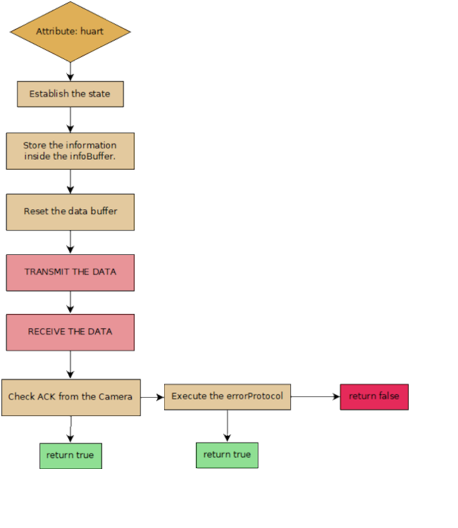](https://wiki.nanosatlab.space/uploads/images/gallery/2024-03/f2usin-titulo.png)
Figure 1: Basic Functions Block Diagram
This scheme can be used for each basic function besides the getData function, at this current point in time., varying the state and the transmit data Buffer and the receive data buffer.
It is known that a general buffer for all the information received can be implemented, but it can also generate numerous problems on the implementation. As it is not necessary to implement and it will complicate the code, different buffers are applied for different data.
The infoBuffer and state variable purpose will be explained in detail in other parts of the documentation.
##### getData
The getData function complexity severely differs from other basic functions due to the implementation of [circular DMA](https://wiki.nanosatlab.space/attachments/416). In contrast to other functions, and due to the structure of the ones used to store data in the flash memory, two relevant buffers have been created in order to store and manage data before flashing. The use of DMA requires callbacks in order to flash data without losing parts of it. In these callbacks, executed when the first buffer is half full and when it is full, will cause an interrupt (not desired but necessary) where the flashing will occur. Here we will make use of an auxiliary buffer in order to copy the second half of the first buffer onto it in order to not cause overlap or flashing of repeated data.
Note that the callbacks are not called when all the data or half is received, they are called in response to the fullness of the buffer (as long as its length coincides with the amount of data specified in the HAL DMA functions). To solve the problem and know how much data shall be received and DMA stopped we make use of the prior fuction, getDataLenght, which will provide us with the total length of the picture. As callbacks are executed, an index will be increased and through comparisons of it, the current callback and the length it'll be determined when to stop the DMA and the execution of the function.
A comprehensive slightly simplified scheme is provided next:
[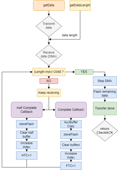](https://wiki.nanosatlab.space/uploads/images/gallery/2024-03/getdata.png)
Figure 2: getData Function Block Diagram
##### **Composite functions**
These functions used different basic functions in order to follow the protocol from the mentioned datasheet.
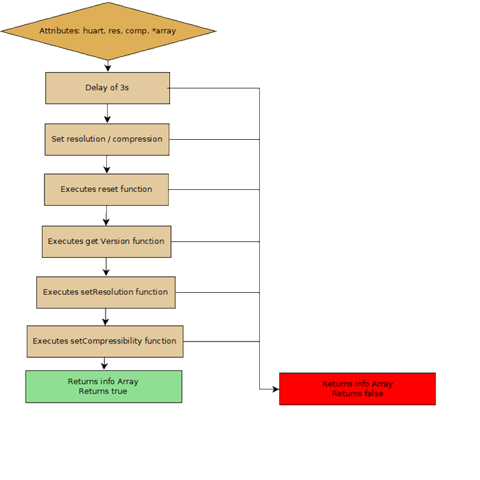
##### initCam
The initCam function initializes the camera with the resolution and the compressibility:
In this case, the initCam is implemented using the huart, the resolution and compressibility needed, and an array in which errors will be stored.
A general scheme of the code is shown below:
[](https://wiki.nanosatlab.space/uploads/images/gallery/2024-03/iAssin-titulo.png)
Figure 3: initCam Block Diagram
##### getPhoto
The getPhoto function is implemented using an UART and an info array attribute. This array is where the buffer of errors will be stored. This function is in charge of executing the order to take the photo, taking it, storing it, and executing the order to stop the camera. A general scheme of the code is shown below:
[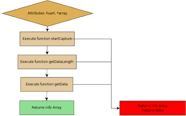](https://wiki.nanosatlab.space/uploads/images/gallery/2024-03/getphoto.png)
Figure 4: getPhoto Block Diagram
# Subsystem Verification
## Camera testing
### How to take and extract an image
In order to take a photo the PTC06 and a STML4, which will be replaced by the OBC-COMMS board in due time, must be connected appropriately. The camera must be provided with a voltage of at least 3.3V to be in working conditions yet it'll work under 5V. A picture of the set-up is provided as well with a diagram which indicates connections to the board.
[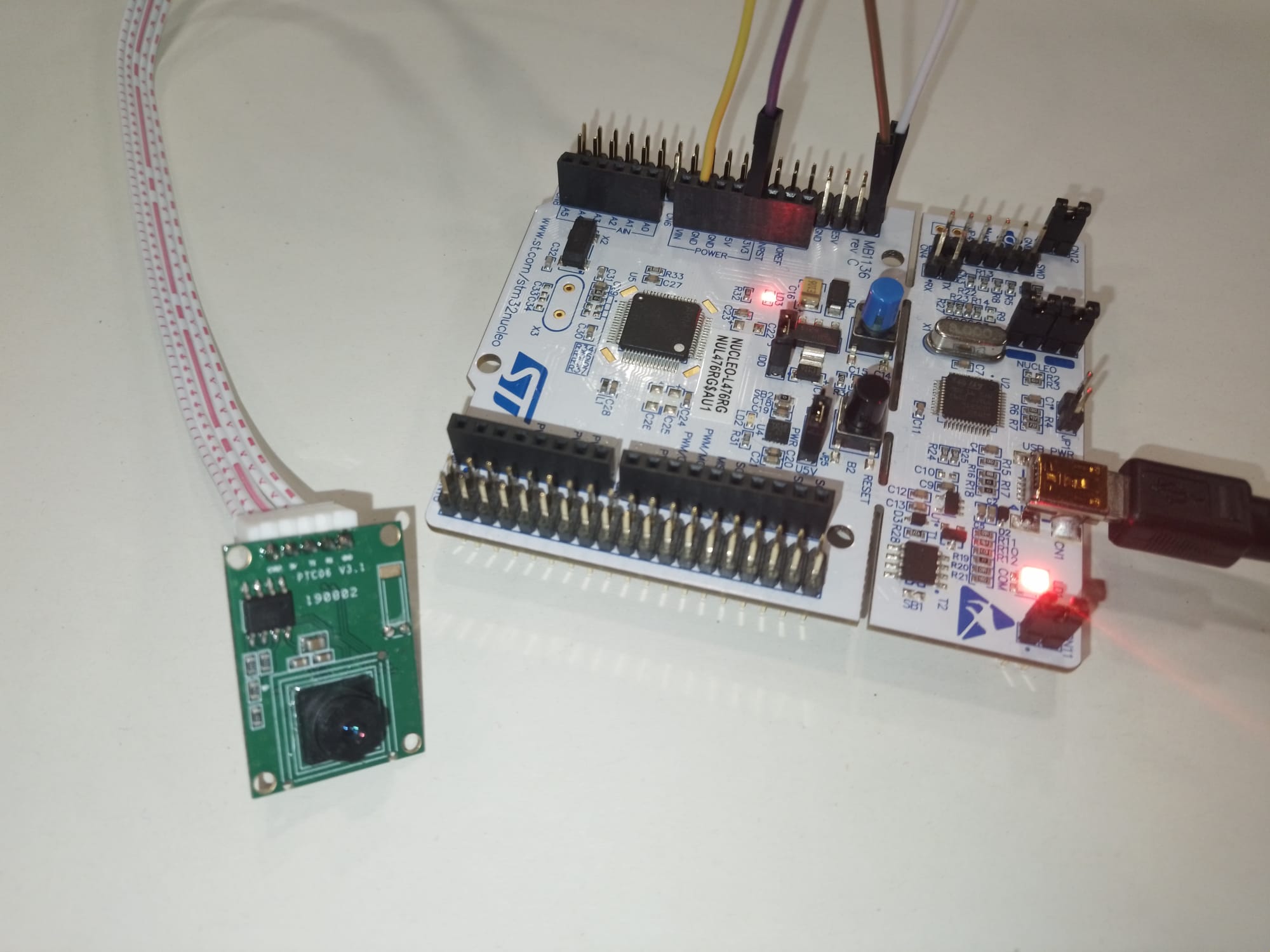](https://wiki.nanosatlab.space/uploads/images/gallery/2024-04/whatsapp-image-2024-04-04-at-10-52-07-am.jpeg)
The following connections must be made between the PTC06 and the STM32:
[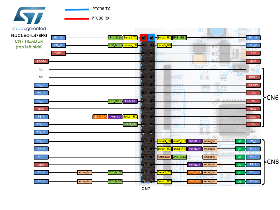](https://wiki.nanosatlab.space/uploads/images/gallery/2024-04/nucleo-l476rg-morpho-left-2017-4-21.png)
[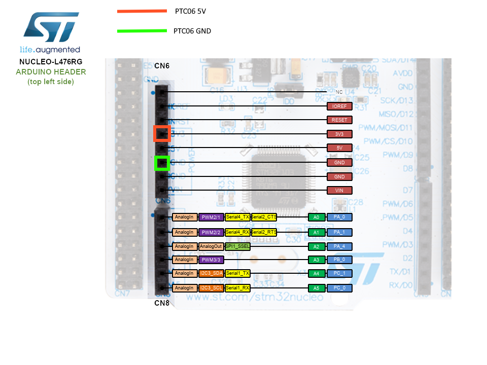](https://wiki.nanosatlab.space/uploads/images/gallery/2024-04/nucleo-l476rg-arduino-left-2017-4-21.png)
Now that the 4 terminals are properly connected the next step is to open the STM32 IDE, and debug the project. Before resuming the debug process it is heavily suggested to check for the variable *'imlenght'* in the expression viewer as well as *'camState'* in the variable expression viewer, so as to know if the process is done.
Resume the debugging and wait until the camera state goes to 'CAM\_STOP\_CAPTURE', now check the hex length of the picture (indicated by the value of the variable *'imlenght'*) and exit the debug session. Now open ST-LINK Utility and enter the address where the pictures is stored (0x08040000, per default in our code) and the size of the picture (should be something along the lines of 0xAAAA). Then connect to the device and save the data as a jpg file. Note that the data should have a D8 byte in the first line and a D9 in the last one.

Obviously this is not an appropriate process to extract pictures from the payload, as it should be done remotely. As of today images can be extracted via COMMS following a Rx-Tx, but this is out of the scope of this document, as taking the picture and storing it appropriately is our only concern for now.
## TEST 1: Image size-quality evaluation
As is to be expected it is necessary to evaluate the trade-off between picture size and quality of an image. So, the goal of this test is to find the most appropriate resolution/compression values considering power and data budget constraints, as we probably won't be able to send full high resolution pictures in a single pass.
Memory size with different values of resolution and compression:
[](https://wiki.nanosatlab.space/uploads/images/gallery/2024-07/untitled-diagram.png)
[](https://wiki.nanosatlab.space/uploads/images/gallery/2024-07/0000.JPG)
[](https://wiki.nanosatlab.space/uploads/images/gallery/2024-07/Puzuntitled-diagram.png)
[](https://wiki.nanosatlab.space/uploads/images/gallery/2024-07/00ff.JPG)
[](https://wiki.nanosatlab.space/uploads/images/gallery/2024-07/Q3Iuntitled-diagram.png)[](https://wiki.nanosatlab.space/uploads/images/gallery/2024-07/0ILe43untitled-diagram.png)
[](https://wiki.nanosatlab.space/uploads/images/gallery/2024-07/11ff.JPG)
[](https://wiki.nanosatlab.space/uploads/images/gallery/2024-07/1100.JPG)[](https://wiki.nanosatlab.space/uploads/images/gallery/2024-07/CCwuntitled-diagram.png)
[](https://wiki.nanosatlab.space/uploads/images/gallery/2024-07/22ff.JPG)

It is complex to assign optimal values to resulution and compression as both can be situational depending on the enviroment that is going to be photographed. Despite this, the trade-off between compression and size is noticeably interesting in higher resolution images. When resolution decreases increasing compression seems to have a less impactful effect, both in image quality and in image size.
It is proposed to adjust both of these parameters according to the situation via telecommands.
## TEST 2: DMA IMAGE TAKING
### Test Description and Objectives
The objective of this test is to verify the implementation of Circular DMA in the data acquisition system of the camera.
### Requirements Verification
| Requirement ID | Description |
|---|
| DIT- 01 | Run the proposed code without errors. |
| DIT- 02 | Take the highest quality image possible by the camera. |
| DIT- 03 | Extract the data successfully from the flash memory of an STM32 Nucleo. |
| Requirement ID | Description |
|---|
| VPN- 01 | All connections are well made, both inside the PCB and to the Nucleo. |
| VPN- 02 | Take an image with the camera. |
| VPN- 03 | Extract the data successfully from the flash memory of an STM32 Nucleo. |
- Nucleo L476RG
- VGA PCB
- PCBite Kit
- Multimeter
| Requirement ID | Description |
|---|
| VOE- 01 | Take an image with the camera. |
| VOE- 02 | Extract the data successfully from the flash memory of the OBC. |
- OBC-COMMS PCB
- VGA PCB
- EGSE (FlatSat)