
| **Component** | **Manufacturer / Supplier** | **Mass (g)** | **Source** |
| **Screws** | |||
| M2x6 Torx ISO14580 | FIXNVIS | 0,2 | Measured |
| M2x20 Torx ISO14580 | FIXNVIS | 0,5 | Measured |
| M2x5 Torx ISO14580 | FIXNVIS | 0,2 | Measured |
| M3x35 Hex ISO7380 | FIXNVIS | 1,7 | Measured |
| **Spacers** | |||
| M3x4 Spacer | RAF Electronic Hardware / MOUSER | 0,2 | Datasheet |
| M3x0.5 Spacer | TORRAS | 0,1 | Measured |
| M2x5 Spacer | Bivar / MOUSER | <0.1 | Datasheet |
| Power Energy | |||
| Solar Cell | Lightricity | 1,4 | Datasheet |
| LiPo Battery | DNK | 34 | Measured |
| **Subsystem and outer PCBs** | |||
| Bottom PCB with components | In-house | 16,6 | Measured |
| Sliding Plate | In-house | 8,4 | Measured |
| Lateral PCB with component | In-house | 11,1 | Measured |
| Y+ Mag PCB with components | In-house | 6,6 | Measured |
| AOCS PCB with components | In-house | 10,2 | Measured |
| EPS PCB with components | In-house | 9,3 | Measured |
| OCB-COMMS PCB with components | In-house | 9,2 | Measured |
| **Structure** | |||
| Bottom structure | PCBWay | 30 | Measured |
| **Payload: K-band** | |||
| K-band antenna | PCBWay | 0,7 | Measured |
| Support FR-4 PCB | PCBWay | 7,6 | Measured |
| RF top PCB with components | PCBWay | ||
| Top structure | PCBWay | 24,3 | Measured |
| RF bottom PCB with components | PCBWay | 9,2 | Measured |
| Interface PCB with components | PCBWay | ||
| **Flat Wires** | |||
| 3 pin PicoBlade - PicoClasp | Molex / MOUSER | 0,3 | Measured |
| 10 pin PicoBlade - PicoClasp | Molex / MOUSER | 1,2 | Measured |
| 15 pin PicoBlade - PicoClasp | Molex / MOUSER | 1,8 | Measured |
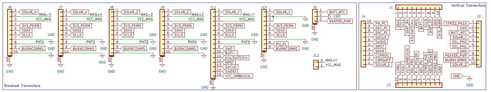
| **Pin Name** | **Connector** | **Pin Number** | **Type** | **Description** |
| SDA1 | J1 | 1 | I2C | I2C1 data bus |
| SCL1 | J1 | 2 | I2C | I2C1 clock bus |
| UART\_RX | J1 | 3 | UART | UART RX bus |
| KILLSWITCH+ | J1 | 4 | Digital | Killswitch positive terminal. |
| PFO | J1 | 5 | Digital Input | Battery fail status pin |
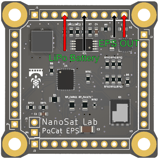
| BATT- | J1 | 6 | Power | Negative terminal of the battery |
| NC | J1 | 7 | Not connected | Free pin for testing & debugging. |
| UART\_TX | J1 | 8 | UART | UART TX bus |
| GND | J1 | 9 | Power | Ground pin |
| VCC | J1 | 10 | Power | General Power line: 3.3V |
| STM32\_PA15 | J2 | 1 | GPIO | Pin connected to STM32 PA15 pin, user defined |
| SWO | J2 | 2 | Serial-Wire Data P | STM32 debug pin |
| BATT\_NTC | J2 | 3 | Analog | Battery temperature NTC sensor |
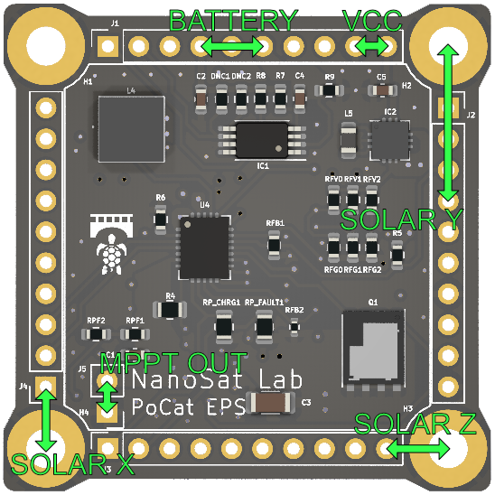
| SOLAR\_Y | J2 | 4 | Power | Solar panel output voltage, Y axis |
| SEL\_PH2 | J2 | 5 | Digital Output | Selector for the photodiode multiplexer |
| SEL\_PH1 | J2 | 6 | Digital Output | Selector for the photodiode multiplexer |
| GND | J2 | 7 | Power | Ground pin |
| HEATER\_PWR | J2 | 8 | Power | Power line that goes to the heater |
| BURNCOMMS | J2 | 9 | Digital Output | COMMS antenna thermal knife enable |
| GND | J2 | 10 | Power | Ground pin |
| SOLAR\_Z | J3 | 1 | Power | Solar panel output voltage, Z axis |
| STM32\_PB0 | J3 | 2 | GPIO | Pin connected to STM32 PB0 pin, user defined |
| ADCS\_POWER | J3 | 3 | Power | ADCS Power line: 3.3V |
| RST\_DRIVERS | J3 | 4 | Digital Input | Active low ADCS current driver reset |
| ADC\_PH | J3 | 5 | Analog Input | Photodiode array output |
| P/L\_POWER | J3 | 6 | Power | Payload Power line: 3.3V |
| SEL\_PH0 | J3 | 7 | Digital Output | Selector for the photodiode multiplexer |
| VCC\_UMBILICAL | J3 | 8 | Power | Umbilical power line |
| FAULT | J3 | 9 | Digital Input | Battery charging fault status pin |
| CHRG | J3 | 10 | Digital Input | Battery charging monitoring pin |
| SOLAR\_X | J4 | 1 | Power | Solar panel output voltage, X axis |
| CHRGOFF | J4 | 2 | Digital Output | Battery charging enable pin |
| CLPROG | J4 | 3 | Analog Input | MPPT output current monitoring pin |
| SDA3 | J4 | 4 | I2C | I2C3 data bus |
| NRST | J4 | 5 | NRST | STM32 NRST signal |
| SWDIO | J4 | 6 | Serial-Wire Data I/O | STM32 debug port |
| SWCLK | J4 | 7 | Serial-Wire Clock | STM32 debug port |
| DAC\_PL | J4 | 8 | Analog Output | STM32 DAC output for payload |
| ADC\_PL | J4 | 9 | Analog Input | STM32 ADC input for payload |
| SCL3 | J4 | 10 | I2C | I2C3 clock bus |
| **Device** | **Bus** | **Address** | **Board** | **Description** |
| TMP112 | I2C1-3.3 V | 1001000 | P/L3 frontend top | Temperature sensor for payload 3 |
| TCN75-P/L2 | I2C1-3.3V | 1001000 | P/L2 frontend bot | Temperature sensor for payload 2 |
| TCN75-Lat +X | I2C3-3.3 V | 1001001 | Lateral +X | Temperature sensor for PQ +X face |
| TCN75-Lat +Z | I2C3-3.3 V | 1001010 | Lateral +Z | Temperature sensor for PQ +Z face |
| TCN75-Lat -X | I2C3-3.3 V | 1001011 | Lateral -X | Temperature sensor for PQ -X face |
| TCN75-Lat -Z | I2C3-3.3 V | 1001100 | Lateral -Z | Temperature sensor for PQ +Z face |
| TCN75-Top +Y | I2C3-3.3 V | 1001101 | Top +Y | Temperature sensor for PQ +Y face |
| TCN75-Bot -Y | I2C3-3.3 V | 1001110 | Bottom -Y | Temperature sensor for PQ -Y face |
| TCN75-ADCS | I2C3-3.3 V | 1001111 | ADCS | Temperature sensor for the magnetorquer drivers |
| BD2606MVV | I2C3-3.3 V | 1100110 | ADCS | Magnetorquer driver |
| MMC5983MA | I2C3-3.3V | 0110000 | ADCS | Magnetometer |
| IIM-42652 | I2C3-3.3 V | 1101000 | ADCS | Inertial Momentum Unit |
| DS2782 | I2C3-3.3 V | 0110100 | EPS | Battery sensor |
In satellite systems, the ADCS is essential to maintain the proper orientation and stability of the spacecraft. This section will initially present the ADCS of the project, presenting some inicial concepts needed for understanding the theory and finishing with some requirements and the physical architecture of the ADCS with other subsystems.
The limited space and power constraints of the PocketQubes pose significant challenges for the design and implementation of subsystems, particularly the ADCS. Thanks to the rapid development of micro-electronics, micro electromechanical systems and integrated circuits, the miniaturization of PQ technology is accelerating.
The ADCS is formed by the attitude determination part, which is the responsible of determine the 3D orientation of the PQ. It uses sensors to obtain information about the environment to determine its orientation. The most common sensors used are magnetometers, Sun sensors, earth sensors, gyroscopes and star trackers. The ADCS that has been developed in this project, is formed by a gyroscope, a magnetometer and photodiodes used as Sun sensors.
Concerning attitude control, it can be achieved passively using magnets located inside the PQ and gravity-gradient stabilization. Additionally, active attitude control can be implemented with actuators such as reaction wheels or magnetorquers. Magnetorquers are the most common actuators used in PQ and will be used in this project. Because of the extremely tight available space, they will be incorporated into the internal layers of the Solar Panels PCBs.
In order to understand this subsystem, some terms must be defined:
It is recommended for the reader to understand a vector as a unique entity in the 3D space. It is essential to distinguish between the vector entity, and the representation of the vector with respect to a frame. The representation of the vector will vary depending.
As an inertial frame, the Earth Centered Inertial frame (ECI) will be used. It is a global cartesian reference frame that has its origin at the center of the Earth.
Figure 1: ECI frame chematic
The body frame will have its origin at the centre of the PocketQube. The axis definition is the following:

Figure 2: Satellite body frame schematic
Quaternions are a mathematical concept equivalent to a rotation matrix. They are used in software for their computational efficiency and to avoid singularities. According to Euler’s Theorem, any rotation is a rotation about a fixed axis, which is represented by the unit vector 𝐞. The angle of rotation is represented by 𝜃. In other words, for any rotation matrix 𝐀, there is a unique 𝐞 and 𝜃 that uniquely define the rotation with respect to the right-hand convention. A quaternion 𝐪 is a four-dimensional vector where the first component is called the scalar part, and the last three components are the vector part. The quaternion is related to the Euler axis-angle in the following manner:

If 𝐴𝑖𝑗 is the element of 𝐀 in its 𝑖-th row and 𝑗-th column, then:


Therefore, a quaternion 𝐪 can be expressed as a function of its rotation matrix 𝐀 using these properties:

Where 𝜀 is the vectorial part of the quaternion. Note that if 𝜃 = 180º, the vector 𝐞 is indeterminate. In such cases, 𝐞 is parallel to any non-zero column of 𝐀. Additionally, it’s crucial to maintain the sign convention.
For any rotation matrix, there exist two corresponding quaternions that differ only in sign. For instance, a rotation of 𝜃 = 180º and another of 𝜃 = 540º are equivalent, but the resulting quaternions are opposite. To uphold the sign convention, it’s necessary to ensure that the scalar part is positive, i.e., to enforce 𝜃 ≦ 180º. This is achieved by changing the sign of the entire quaternion if the scalar part is negative.
There is an essential property for achieving attitude control in the ADCS. If there are two quaternions, q1 and q2, and q1 is conjugated and then multiplied by q2, the resulting quaternion represents the relative rotation between the two quaternions.

In this case qerror would be the quaternion that represents the rotation needed to align q1 to q2. The qerror can also be named error quaternion.
An orbital propagator is used to determine the position and velocity of the satellite at a given instant of time, given by the initial position of the satellite and the velocity at this position. In the satellite we are using the J2 propagator, whose main property is
that it accounts for the Earth’s oblateness while propagating the orbit. Additionally, this propagator is ideally for our PQ because of the balance of memory requirements and complexity fits in the OBC.
There are more precise orbital propagators like the SGP4 model which accounts for atmospheric drag and other secular effects apart from the Earth oblateness, but it is much more complex, and it requires more memory than the one available in our satellite.
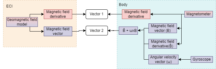
The geomagnetic field model is essential for calculating the Earth’s magnetic field at specific coordinates and dates. This model helps to understand and predict the variations in the Earth’s magnetic field. In this work, the IGRF model is used, but simplified up to order 2 , commonly referred to as the Tilted Dipole model. The Tilted Dipole model approximates the Earth’s magnetic field as a dipole that is tilted relative to the Earth’s rotational axis. Despite its simplicity, this model provides a reasonably accurate representation of the geomagnetic field for many practical purposes. The coefficients for the Tilted Dipole model are derived from the IGRF model, which is updated every five years based on satellite and ground-based observations .

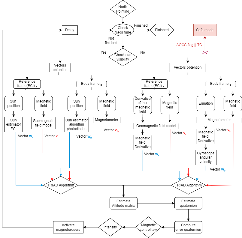
Figure 3: ADCS functional architecture schematic with the rest of the subsystems
The ADCS in the PocketQube serves as an interface between the outer boards and the inner PCBs of the satellite. As shown in [Figure 3], the ADCS is connected to three main structural components: the outer boards, the inner +Y magnetorquer PCB, and the on-board computer (OBC).
On the outer boards, there are magnetorquers used for the ±X, -Y, and ±Z axis, photodiodes, and some temperature sensors. Additionally, the +Y magnetorquer is connected just below the ADCS PCB. This location is chosen due to space constraints within the PocketQube, as it is not optimal to place it on the top board, where the payload will be inserted.
Finally, the ADCS is connected to the OBC, which is responsible for processing all data gathered by the ADCS. The connections between the ADCS and the OBC are not simple power lines each has a specific function:
| SS | ID | DESCRIPTION |
|---|---|---|
| ADCS | ADCS-0000 | The communication between the chips of the ADCS and the OBC must be conducted via I2C. |
| ADCS | ADCS-0010 | The PQ must be able to detumble using the BDOT algorithm. |
| ADCS | ADCS-0020 | The satellite must be able to point the Payload at the nadir angle using the magnetic control law. |
| ADCS | ADCS-0030 | The ADCS must be able to estimate the satellite's position in an inertial reference frame. |
| ADCS | ADCS-0040 | The ADCS must be able to obtain the magnetic field in an inertial reference frame. |
| ADCS | ADCS-0050 | All sensors used in the ADCS must be calibrated and characterized by temperature. |
| ADCS | ADCS-0060 | The magnetorquers must have a reliable current supply to ensure optimal performance. |
| ADCS | ADCS-0070 | The ADCS must have a fail-safe mechanism to enter a safe mode in case of anomalies. |
| ADCS | ADCS-0080 | The ADCS sensor's calibration parameters must be able to be modified via telecommand. |
The hardware of the Attitude Determination and Control System (ADCS) is essential for the satellite’s operation. Without it, the satellite would be unable to gather critical data about its orientation and environment in space, which is necessary for executing various functions. The ADCS hardware enables the satellite to determine its position, control its orientation, and stabilize itself, ensuring that it can carry out mission objectives such as data collection and communication.
The design of the ADCS follows a simple philosophy, all components and sensors are selected for their low power use, good performance, and reasonable cost. The goal was to choose parts that are reliable and fit within the PocketQube’s limited power and budget.
There were several options for implementing an actuator in the PocketQube. As explained in the ADCS introduction section, there are two ways to achieve attitude control: passive control, using a magnet as an actuator, and active control, using reaction wheels or magnetorquers.
The passive option was considered, as it is the primary method used for achieving attitude control. However, one drawback of this approach is the limited control over pointing precision.
For the active option, using reaction wheels was discarded because the size and power consumption requirements of a PocketQube are incompatible with this approach. Thus, the remaining option for active attitude control was the magnetorquers. This technique is relatively new, and this would be one of the first PocketQubes to implement it. Additionally, it offers the pointing accuracy needed to conduct the required measurements. For these reasons, magnetorquers were chosen.
Regarding the sensors, the main objective was to find ones compatible with the I2C protocol.
The I2C protocol is mainly used for enabling communication between multiple integrated circuits on the same board with minimal wiring. It is based on a two-wire serial communication protocol, which uses one line for data, called SDA, and another for the clock signal, called SCL, allowing for simple, low-speed data exchange over short distances.
I2C is used in applications where several peripheral devices (like sensors, memory devices, or display drivers) need to communicate with a central microcontroller or processor. It also has low power consumption, which is crucial in satellite applications.
The magnetometer IC that will be used for the ADCS is the MMC5983MA, developed by MEMSIC, is a high-precision, 3-axis magnetometer known for its small size and low power consumption, making it particularly suitable for small satellite applications like PocketQubes. Datasheet: MMC5983MA
|
Attribute |
Specification |
|---|---|
|
Name |
MMC5983MA |
|
Supplier/Manufacturer |
Mouser, Memsic |
|
Power Consumption |
212.19 μW |
|
Field Range |
± 8 G |
|
Resolution |
0.25 mG per LSB |
|
Operation Bits |
16 bits |
|
Sensitivity |
± 4096 Counts/G |
|
RMS Noise |
0.4 mG |
The Gyroscope IC that will be used for the ADCS is the IIM-42652, manufactured by TDK InvenSense, is a compact, high-performance 6-axis Inertial Measurement Unit (IMU) combining a 3-axis accelerometer and 3-axis gyroscope. Its design and capabilities make it well-suited for small satellites like PocketQubes, which require efficient, low-power, and reliable orientation and motion data for various tasks such as attitude determination, stabilization, and control. Datasheet: IIM-42652
|
Attribute |
Specification |
|---|---|
|
Name |
IIM-42652 |
|
Supplier/Manufacturer |
Mouser, TDK InvenSense |
|
Power Consumption |
1.91 mW |
|
Scale Range |
±15.625 °/s, ±31.25 °/s, ±62.5 °/s, ±125 °/s, ±250 °/s |
|
Operation Bits |
16 bits |
|
Sensitivity Scale Factor |
2097.2 LSB/(°/s), 1048.6 LSB/(°/s), 524.3 LSB/(°/s), 262 LSB/(°/s), ç 131 LSB/(°/s) |
|
RMS Noise |
0.038 °/s-rms |
The temperature sensors that will be used are named TCN75A, createdby Microchip Technology, designed for low-power applications and precise temperature measurement. Its compact size, low power usage, and simplicity make it suitable for use in small satellite platforms like PocketQubes, especially where basic thermal monitoring is needed. Datasheet: TCN75AVOA
|
Attribute |
Specification |
|---|---|
|
Name |
TCN75A |
|
Supplier/Manufacturer |
Mouser, Microchip Technology |
|
Power Consumption |
1.65 mW |
|
Field Range |
-40 °C to 125 °C |
|
Accuracy |
±1 °C |
|
Resolution |
0.0625 °C to 0.5 °C |
|
Operation Bits |
16 bits |

The SLCD-61N8 is a reliable and cost-effective silicon photodiode designed for light sensing and power generation. It provides visible to infrared sensitivity, high efficiency, low capacitance, and excellent durability. The choice of photodiode is flexible, and alternative models with similar wavelength sensitivity to sunlight can also be considered for use. Datasheet: SLCD-61N8
|
Attribute |
Specification |
|---|---|
|
Name |
SLCD-61N8 |
|
Supplier/Manufacturer |
Mouser, Advanced Photonix |
|
Short Circuit Current |
170 μA |
|
Open Circuit Voltage |
0.4 V |
|
Maximum Sensitivity Wavelength |
930 nm |
|
Acceptance Half Angle |
60 deg |

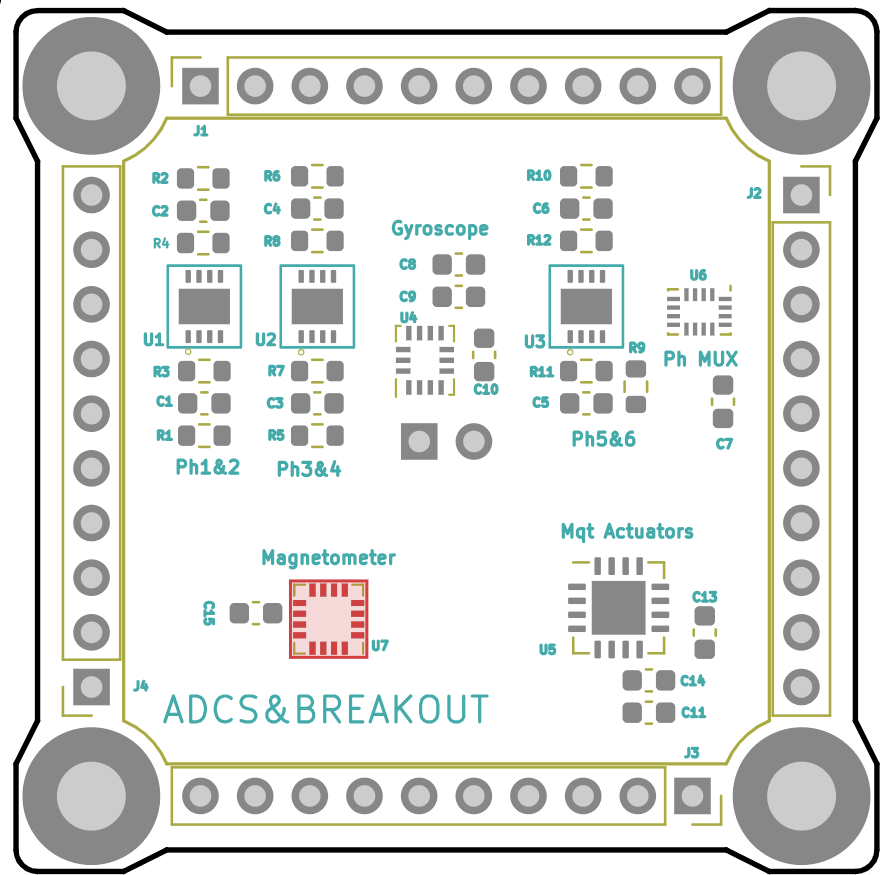
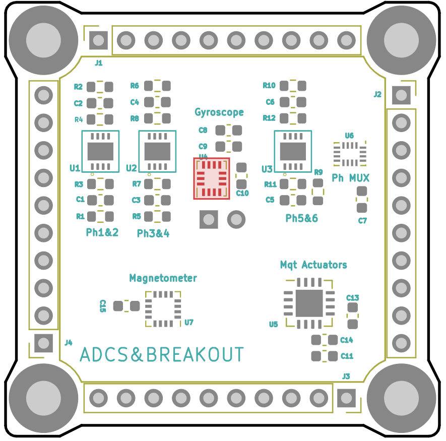
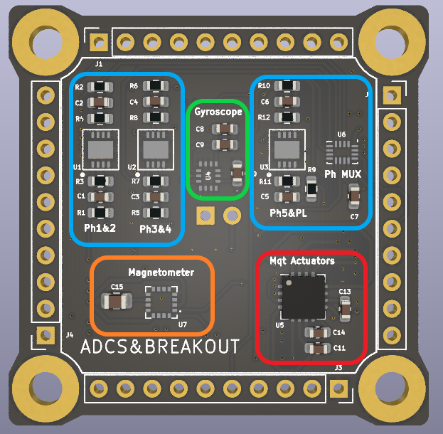
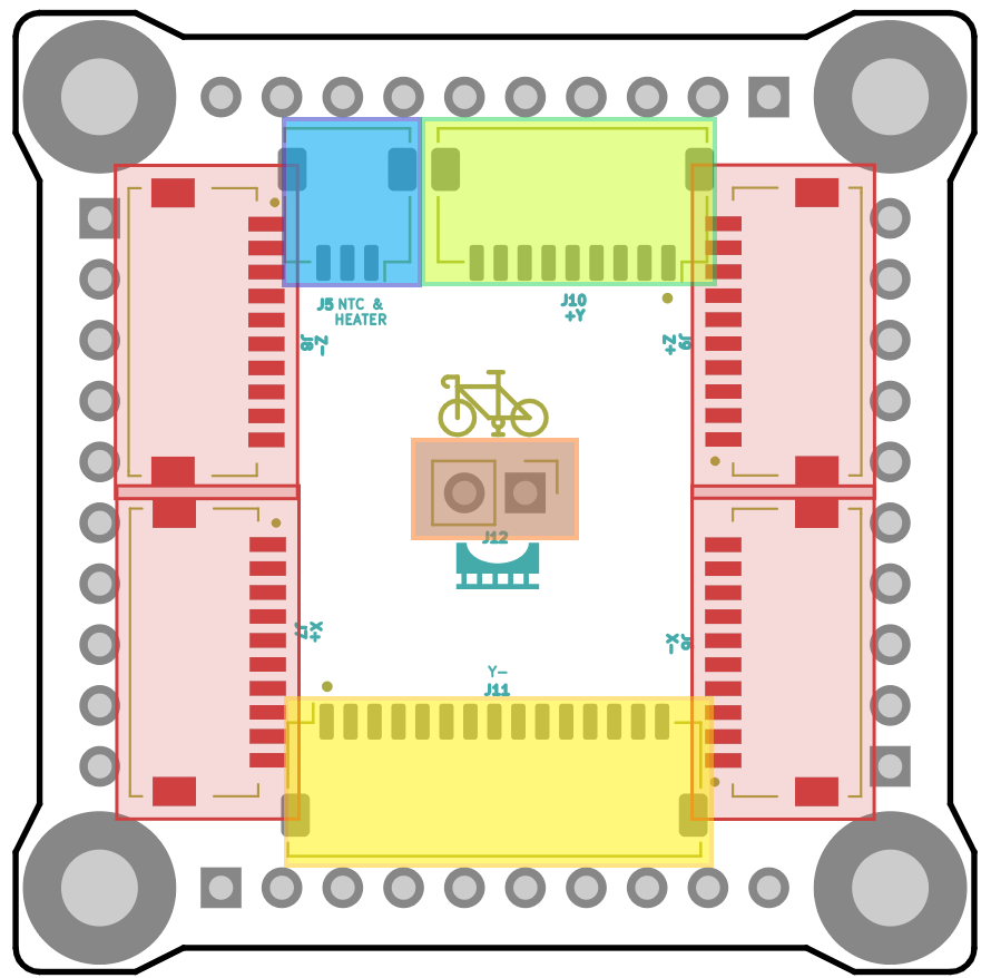
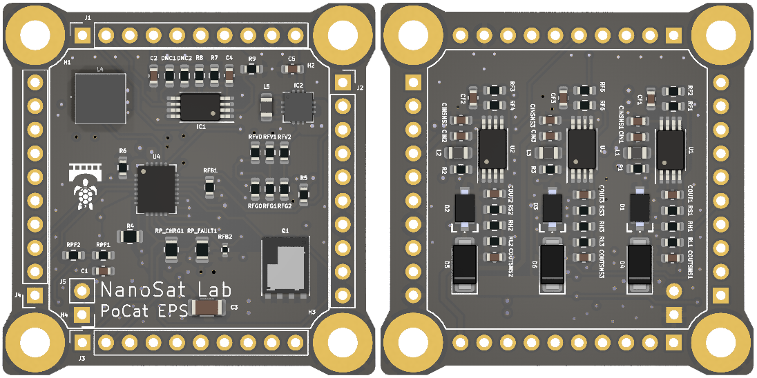
This is the PCB design of the ADCS. The board is also used as an interface between the other subsystems and the outer boards and the battery. It is divided into 5 different blocs.

|
Component |
Type |
Quantity |
Manufacturer number |
|
Component |
Type |
Quantity |
Manufacturer number |
A more detailed information about each vertical PIN and bottom pin is shown in the following picture:
The magnetorquers are responsible for achieving attitude control in the PQ. These devices function as magnetic dipoles and when an electric current is passed through them, they create a magnetic moment. This magnetic moment interacts with the Earth’s magnetic field, generating a torque that adjusts the satellite’s orientation. This interaction can be represented as:
![]()
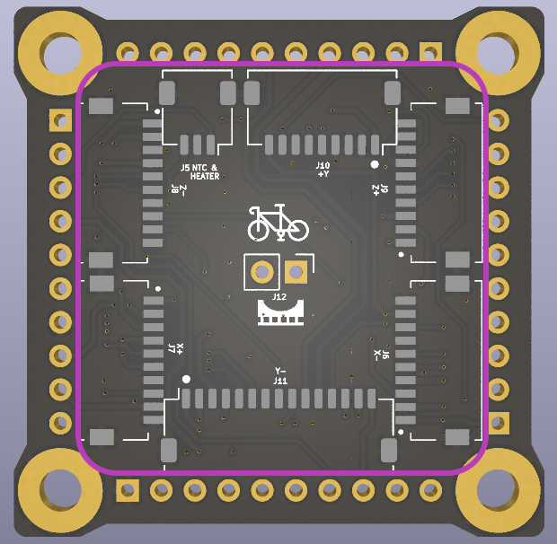
The calculation of the magnetic moment depends on the type of magnetorquer used. In the PocketQube, planar helical coils serve as magnetorquers, embedded in the outer boards along each axis, except for the +Y axis, where they are positioned within the inner layers of the satellite. These coils are distributed across the boards in four layers.

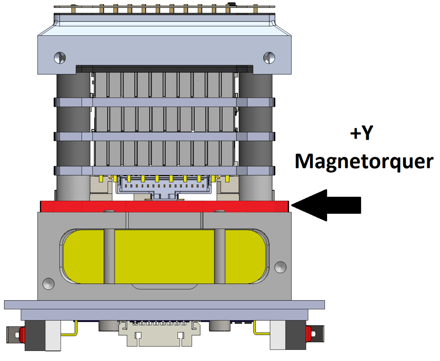
|
|
+Y PCB |
Lateral & Bottom |
|
Separation between turns |
0.2 mm |
0.2 mm |
|
Height |
35 µm |
35 µm |
|
Width of the trail |
0.18 cm |
0.18 cm |
|
Material of the trail |
Copper |
Copper |
|
Dimensions |
28 x 28 mm |
32 x 32 mm |
|
Resistance |
89.91 Ω |
88.3 Ω |
|
Turns per layer |
42 |
38 |
|
Maximum moment |
3.63·E03 a·m^2 |
3.2·E03 a·m^22 |
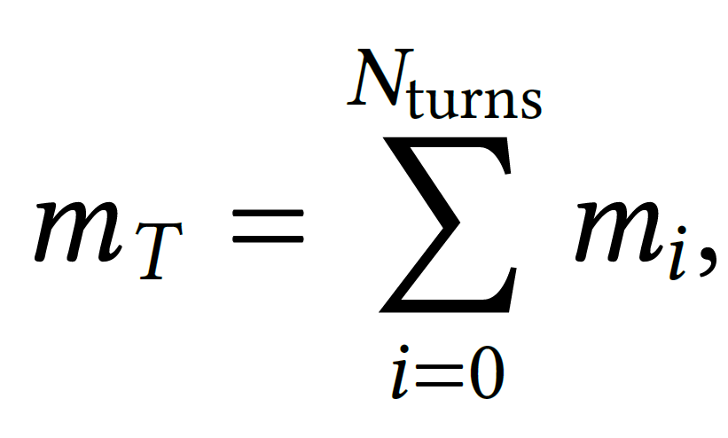
In order to compute the intensity, firstly the total magnetic moment expression shall be derivated. The magnetic moment of a coil is,

As we have a combination of coils the total magnetic moment will be,
To compute the total magnetic moment, the magnetorquer coils will be modeled as square coils, with each turn represented as an individual square coil,

These coils are separated by distances 𝐝outer = 0.2 mm and 𝐝top = 0.18 mm. The label, "outer" refers to the magnetorquers located on the outer boards, and the label "inner" refers to the magnetorquer located inside the satellite.
The total magnetic moment of the magnetorquers will be computed as:
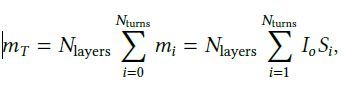
Where 𝐍layers is the number of layers of the magnetorquer, 𝐈o is the required injected intensity, and 𝐒𝐢 the surface ofthe coil with the turn number 𝐢. The expression that calculates the surface of each turn is:
![]()
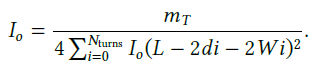
where 𝐋 is the size of the bigger coil and 𝐖𝐢 the amplitude of the conductor of the coil. In addition 𝐝𝐢 and 𝐖𝐢 can be 𝐝𝐢(𝐢𝐧𝐧𝐞𝐫), 𝐝𝐢(𝐭𝐨𝐩), 𝐖𝐢(𝐢𝐧𝐧𝐞𝐫), 𝐖𝐢(𝐭𝐨𝐩). Isolating the required current from the equation we obtain that:
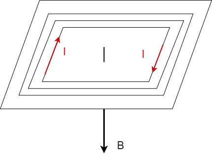
Finally one of the most important things to characterize of the magnetorquers is their polarisation. The polarisation of a coil refers to the direction of the magnetic fiel generated when some intensity is injected throught the coils. The polarisation should follow the right hand rule.
In our case as shown in,
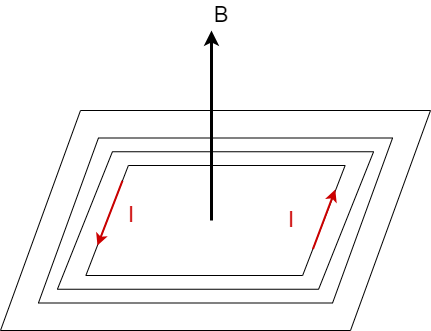
If the current flows clockwise, the magnetic field direction is perpendicular towards the bottom face of the plane formed by the coils of the magnetorquer. Similarly, if the current flows counterclockwise, the magnetic field direction is perpendicular towards the top face of the plane,
The software of the Attitude Determination and Control System (ADCS) is equally essential for the satellite’s operation. Without it, the satellite would lack the intelligence to interpret critical data about its orientation and respond to its environment in space, which is necessary for executing various functions. The ADCS software processes sensor data, executes algorithms to determine the satellite's position, and issues commands to control and stabilize its orientation. This ensures that the satellite can reliably carry out mission objectives such as precise data collection, alignment with targets, and consistent communication.
The attitude of the satellite is represented mathematically as the rotation matrix, which stores the information about the orientation of the satellite. The objective of the ADCS is to calculate that matrix and later conduct some functionalities to achieve the desired orientation.
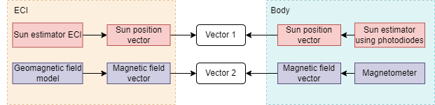
To calculate the rotation matrix, the idea is to obtain two type of vectors, each one of them represented in two different frames, the ECI and the body frame. Once we obtain these vector the following system of equations shall be solved :
 where subscript 1 represents the first vector, subscript 2 represents the second vector, r denotes the reference frame, and b denotes the body frame and the symbol A refers to the rotation matrix. Since this system of equations is undetermined, the rotation matrix cannot be directly computed and must be estimated. In order to estimate it, the TRIAD algorithm will be used.
The TRIAD algorith is based on the assumption that one of the unit vectors is much more accurately determined than the other. It denotes that 𝐛𝟏 is much more accurated than the others. The estimation of the rotation matrix is shown in,
![]()
![]()
The criteria chosed to select the vectors is the following one:
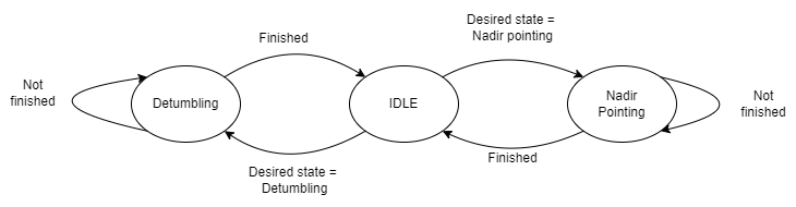
The former AOCS modes of operations available in the PocketQube are the Detumbling mode, Nadir pointing and the IDLE mode. The primary purpose of the ADCS implementation is to prevent unnecessary energy consumption. If no AOCS functions are needed, the task will remain blocked until required, it will be activated by the onboard computer only when necessary.
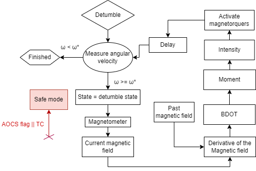
After the deployment from the rocket, the PQ is expected to start rotating at an average rate of 30 degrees per second. In addition, the PQ will be influenced by various external forces during its orbit, causing it to start rotating, and intentional rotations will be applied to the PQ to manage its temperature more efficiently. Because of these factors its necessary a functionality that permits to detumble the satellite. This mode will be used in the following situations:
The detumbling mode uses the BDOT controller. For determining the value of the constant used in the BDOT algorithm, the BDOT law method will be used, which uses the maximum magnetic moment that will be generated by the magnetorquers and the sign of the derivative of the measured magnetic field. This maximum magnetic moment is computed taking into account that the maximum intensity that the magnetorquer driver can provide to the magnetorquers is of 32 mA.
![]()
In order to perform correctly the measurements of the payload antenna, the PQ must be pointing to the Earth. Nadir pointing is the most crucial functionality of the ADCS, because it is the responsible of pointing the satellite to the Earth. For achieving it a magnetic control law is used. It computes the desired magnetic moment using the magnetic field, the angular velocity and the vectorial part of the required quaternion that is needed for rotating the satellite’s quaternion to the required quaternion.
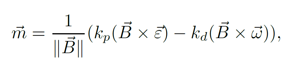
where the constants 𝐤𝐩 and 𝐤𝐫 are obtained from the PID controller, and the 𝜺 represents the vectorial part of the error quaternion.
The IDLE mode is the default mode, this mode is always set whenever the AOCS is not running any functionality. In addition, this is the only mode where the On board computer will be able to block the AOCS task to prevent undesired energy consumption.
In the PocketQube, the geomagnetic field model that is implemented is a simple Tilted dipole model. This is due to memory limitations in the PocketQube. The tilted dipole is a simplified model of the IGRF13 with only two coefficients. However, if additional memory is available, the possibility of adding more coefficients will be considered.
| Inputs | Outputs |
| Geodetic coordinates | Magnetic field in ECI [nT] |
| Decimal year |
The orbital propagator used for the PocketQube is the J2 orbital propagator. The algorithm estimates the orbit in ECI coordinates using the TLE received from the ground station. Due to memory limitations, this propagator is chosen, but using a more accurate one will be considered if memory permits.
| Inputs | Outputs |
| Satellite TLE | Satellite propagated orbit in ECI |
| Desired propagated time [hours] |
In the PocketQube, two different methods are used to determine the sun’s position, one in the ECI frame and another in the body frame. Hence, two algorithms are implemented:
| Inputs | Outputs |
| Date | Sun position ECI |
| Inputs | Outputs |
| Received light from photodiodes | Sun position in body frame |
| Temperature of latera, bottom and top boards |
| Requirement ID | Description |
|---|---|
| ADCS - SSV - 00 | All external physical aspects, such as scratches, soldering, or joint issues, of the PCB must be inspected. |
| ADCS - SSV - 01 | Each lateral pin must establish a secure connection. |
| ADCS -SSV - 02 | All active components must be ensured to operate correctly, with no short circuits or open connections, and each pin, must meet the specified value. |
| ADCS -SSV - 03 | The positioning and fitment of each component mounted on the PCB must be verified. |
| **Step ID** | **Description** |
| Test1 - 10 | With the help of the microscope, look at the PCB looking for any outer physical parameters, such as scratches, soldering or joint issues. If any anomaly is detected, re-solder or fix the encountered error. |
| Test1 - 20 | Check the correct connection with the corresponding component of the 40 pins (10 in each lateral side) with the multi-meter. |
| Test1 - 30 | Check the value with the multi-meter of all the passive components and compare it to the one in the schematic. |
| Test1 - 40 | Verify the active components, checking one by one all the pins with the multi-meter in order to find shorts, open ends, and correct connections among the various pins. |
| Test1 - 50 | Check the connections between all of the components and pins of the PCB. |
| Requirement ID | Description |
|---|---|
| ADCS - SSV - 10 | The gyroscope must be tested using a reliable tool capable of reproducing constant angular velocities accurately. |
| ADCS - SSV - 11 | The gyroscope must be able to switch between specific full scale ranges of angular velocities. |
| ADCS - SSV - 12 | The gyroscope produced bits, must be translated in degrees per second or radians per second. |
| ADCS - SSV - 13 | The data from the gyroscope must closely match the theoretical value corresponding to the rotation of the rotary platform. |
| **Step ID** | **Description** |
| Test2 - 10 | Connect the power supply to the STM32 nucleoboard. |
| Test2 - 20 | Open the STM32CubeIDE program. |
| Test2 - 30 | Prepare a code that can read from the gyroscope using I2C. |
| Test2 - 40 | Connect the nucleoboard to the ADCS PCB correctly. |
| Test2 - 50 | Run the code into the nucleoboard in the debug mode checking step by step if the connection with the ADCS board is working correctly. |
| Test2 - 60 | Connect the rotating platform with motor to the power supply, inject the voltage and intensity needed for the proper operation of the engine. |
| Test2 - 70 | Place the gyroscope in the rotation platform and run the code. Write down the values of the data. |
| Test2 - 80 | Measure with the chronometer how long the platform takes in rotating 360 degrees, then compute how many degrees per second it is equivalent to. |
| Test2 - 90 | If the values of the gyroscope and the computed value corresponds with the values computed before, the gyroscope is working correctly. |
| **REGISTER NAME** | **ADDRESS** | **FUNCTION** |
| SENSOR\_CONFIG0 | 0x03 | Disables and enables the gyroscope axis. |
| PWR\_MGMT0 | 0x4E | Enables and disables all sensors of the chip. We are only enabling the temperature sensor and the gyroscope. |
| GYRO\_CONFIG\_STATIC2 | 0x0B | Disables and enables Anti-Aliasing/low pass filter and notch filter. In our case we are using only the Anti-aliasing and low pass filter. |
| GYRO\_CONFIG0 | 0x4F | Configuration register for the gyroscope, the full scale range and the ODR frequency can be modified. We are using the default frequency of the ODR and a full scale range that fluctuates depending on the situation (this can't be configurated via registers, it has to be coded). |
| GYRO\_DATA\_X1/X0 | 0x25/0x26 | X1: Upper byte of Gyro X-axis data. X0: Lower byte of Gyro X-axis data. |
| GYRO\_DATA\_Y1/X0 | 0x27/0x28 | X1: Upper byte of Gyro Y-axis data. X0: Lower byte of Gyro Y-axis data. |
| GYRO\_DATA\_Z1/X0 | 0x29/0x2A | X1: Upper byte of Gyro Z-axis data. X0: Lower byte of Gyro Z-axis data. |
| TEMP\_DATA1/0 | 0x1D/0x1E | X1: Upper byte of temperature data. X0: Lower byte of temperature data. |
The obtained data is not calibrated, therefore, a calibration test has been made.
### Conclusions With all requirements met, the gyroscope has successfully passed the test, and the ADCS PCB is now prepared for further testing. --- ## TEST 3: Magnetometer ### Test Description and Objectives The purpose of this test is to validate that the Magnetometer integrated into the PCB operates in accordance with the specified requirements and successfully communicates with the computer using the I2C protocol. This includes assessing the Magnetometer's performance metrics and ensuring reliable data transmission between the Magnetometer and the computer. ### Requirements Verification| Requirement ID | Description |
|---|---|
| ADCS - SSV - 20 | The magnetometer data for each axis should display an elliptical shape. |
| ADCS - SSV - 21 | Test measurements should be conducted in an area free from any potential magnetic sources. |
| **Step ID** | **Description** |
| Test3 - 10 | Prepare the power supply with 3.3V and 800mA. |
| Test3 - 20 | Connect the power supply to the PCB. |
| Test3 - 30 | With the help of the multimeter, check that the VCC inputs pins has the correct value. |
| Test3 - 40 | Disconnect the power supply and turn it off. |
| Test3 - 50 | Turn on the computer and open the STM32CubeIDE program. |
| Test3 - 60 | Prepare a code that can read from the magnetometer using I2C. |
| Test3 - 70 | Connect the nucleoboard to the ADCS PCB using SCL and SDA pins. |
| Test3 - 80 | Run the code into the nucleoboard and look in the memory register to see if the communication between the nucleo and the PCB has been done. |
| Test3 - 90 | Run again the code and conduct measurements of the magnetometer being rotated randomly to all directions. |
| **REGISTER NAME** | **ADDRESS** | **FUNCTION** |
| Internal Control 0 | 0x09 | This register is mainly used for initiating a measurement event of the magnetic field or the temperature. Among other things. |
| Status | 0x08 | This register is used for checking if the measurement event of the magnetic field or the emperature, is completed. |
| Xout0, Yout0, Zout0 | 0x00, 0x02, 0x04 | X,Y,Z-axis output in unsigned format. Bits \[17:10\] |
| Xout1, Yout1, Zout1 | 0x01, 0x03, 0x05 | X,Y,Z-axis output in unsigned format. Bits \[9:2\] |
| XYZout2 | 0x06 | X,Y,Z-axis output in unsigned format. Bits \[1:0\] |
The obtained data is not calibrated, therefore, a calibration test has been made.
### Anomalies With the electrical test complete and all hardware functioning properly, if measurements remain unchanged or varely do not change. Try exciting the magnetometer with a magnet. Bring the magnet close to the magnetometer chip and rotate the PCB randomly. This should resolve the issue. ### Conclusions With all requirements met, the gyroscope has successfully passed the test, and the ADCS PCB is now prepared for further testing. --- ## TEST 4: Photodiode and Operational Amplifiers ### Test Description and Objectives The purpose of this test is to validate that the Photodiodes integrated into the lateral boards operate in accordance with the specified requirements. The Photodiodes block include the Operational amplifiers and also the photodiode multiplexer. The test involves evaluating the performance metrics of the photodiode and ensuring dependable data transmission between the magnetometer and the computer. ### Requirements Verification| Requirement ID | Description |
|---|---|
| ADCS - SSV - 30 | The photodiodes must only generate current proportional to the exposed light source. If there is no light source the photodiode must not generate any current. |
| ADCS - SSV - 31 | The operational amplifiers must convert the provided intensity of the photodiodes into voltage and amplify the signal. |
| ADCS - SSV - 32 | The analog to digital converter of the STM32 must convert the output of the operational amplifiers into bits. |
| **Step ID** | **Description** |
| Test4 - 10 | Prepare the black coated box with the halogen bulb inside in one side of the box. |
| Test4 - 20 | On the other side prepare the photodiode on the rotating platform pinting towards the halogen bulb. |
| Test4 - 30 | Turn on the bulb and measure the output value with the help of a multimeter. |
| Test4 - 40 | Connect the photodiode to the operational amplifier and repeat stem 3. |
| Test4 - 50 | Connect the rotating platform to a power supply and do a complete round measuring the data and storing it in the computer. You can use the Analogic inputs from the STM32 board. |
| Test4 - 60 | Repeat the previous step, but in this case with the platform rotating in the opposite direction. |
| Test4 - 70 | Repeat step 4. and 5. rotating the photodiode 90 degrees. |
| Test4 - 80 | Plot the results. |
| Requirement ID | Description |
|---|---|
| ADCS - 31 | Sensor correctly supplied with 3.3V |
| ADCS - 32 | The device need to establish a connection with the computer using I2C |
| ADCS - 33 | The output values of the magnetorquer actuator block must be a constant current, with the specified value |
| **Step ID** | **Description** |
| Test5 - 10 | Prepare the power supply with 3.3V and 800mA. |
| Test5 - 20 | Connect the power supply to the PCB using the ADCS\_POWER input. |
| Test5 - 30 | With the help of the multimeter, check that the VCC inputs pins has the correct value. |
| Test5 - 40 | Disconnect the power supply and turn it off. |
| Test5 - 50 | Turn on the computer and open the STM32CubeIDE program. |
| Test5 - 60 | Prepare a code that can configure the output values and pins of the BD2606MVV. |
| Test5 - 70 | Connect the nucleoboard to the ADCS PCB using SCL and SDA pins. |
| Test5 - 80 | Run the code into the nucleoboard and look that the write and read functions return a "HAL\_OK" value, confirming the correct communication. |
| Test5 - 90 | Disconnect the nucleo board. |
| Test5 - 100 | Connect a protoboard to the output LEDA1 and to the 10K Ohms resistance. |
| Test5 - 110 | Prepare the code in order to configure the output with 1 mA and to the output LEDA1. |
| Test5 - 120 | Connect the nucleo board and run the code. |
| Test5 - 130 | With the help of the multimeter validate that the current is 1 mA. |
| Test5 - 140 | Disconnect the nucleo board and change the resistance to the 20 Ohms one. |
| Test5 - 150 | Connect the nucleo board and run the code. |
| Test5 - 160 | With the help of the multimeter validate that the current is still 1mA. |
| Test5 - 170 | Repeat the same process with the 30 Ohms resistance. |
| Test5 - 180 | Repeat the steps from 9 to 17 with the 6 outputs and for current valors of 10 mA, 20 mA and 35 mA. |
There is a problem with the I2C communication that makes the code fail. To solve this problem the next tests has been done:
1. Verify the connections
All the I2C connections are well connected with the corresponding PINS
2. Check the components
The components connected are the corresponding ones and in the correct positions according to the Ki Cad schematic. Furthermore no component has any short circuit.
3. Verify the addresses of the device
The device address is the correct one. It can be seen in the I2C Addresses document of the nanosatlab wiki or in the datasheet of the device
4. Check step by step that all the connections are working fine
The EPS is responsible for managing the energy throughout the satellite, including charging the battery and distributing power to the various subsystems. It is divided into two main blocks: the Energy Harvest Block, which is in charge of collecting energy from the solar cells and maximizing power generation, and the Battery Charger Block, which efficiently and safely charges the LiPo battery while distributing power to the different subsystems.
It is made use of a total of 5 solar cells: 4 on the sides and 1 on the bottom. These are high-efficiency GaAs triple junction solar cells with an efficiency rate of 30%. The solar cells on the sides are arranged in parallel (+Z with -Z and +X with -X). This configuration allows one of the two faces to always be illuminated, enabling the use of one MPPT (Maximum Power Point Tracker) for each pair of solar cells. The bottom cell is managed individually with its own MPPT.
The MPPTs are responsible for maximizing the power generated by the solar cells. After the MPPT output, with a reverse-blocking diode, the power management system will handle the energy distribution.
The Power Management IC is the core component that manages energy at all times, deciding the actions based on the available energy and the requirements of the other subsystems. Depending on the battery’s charge state, the Power Management IC will take advantage of the opportunity to charge it, ensuring that energy is always available.
Simultaneously, energy is constantly sent through a power regulator, reducing the voltage to 3.3V, which is used by the other subsystems. The Power Management IC will decide whether to power the system directly from the solar cells, depending on the power consumption, or from the battery when necessary.
The EPS also includes a battery sensor capable of measuring various battery parameters such as voltage, current and temperature. This sensor communicates with the OBC via I2C. Additionally, the battery is equipped with an NTC temperature sensor that the Power Management IC can read to ensure the battery does not overheat or drop below a certain threshold. If the OBC detects that the battery temperature approaches a critical level, it will activate a battery heater to maintain the temperature within safe operating limits
Moreover, the Power Management IC, through digital control pins, will notify the OBC of its status, including notifications such as charge completed or battery error, among others.
To the other subsystems, the EPS appears as a single power source, capable of providing the necessary energy at all times while also supplying real-time battery data.
A block diagram of the EPS is provided up next:

Figure 1: EPS Block Diagram
The EPS is designed and schedulled tu fulfill the following requirements established by the necessitities of the spacecraft and the mission itself.
| SS | SS - Number | DESCRIPTION |
|---|---|---|
| EPS | EPS-0000 | The EPS is capable of providing the requisite current for the other subsystems to function correctly. |
| EPS | EPS-0010 | The battery shall remain within safe temperature ranges. |
| EPS | EPS-0020 | The EPS shall provide an output of 3.3V ±5% at its output to power the other subsystems |
| EPS | EPS-0030 | The battery shall be able to charge via the umbilical port. |
| EPS | EPS-0040 | The satellite's battery shall be decoupled from the rest of the system during launch using mechanically controlled kill switches. |
| EPS | EPS-0050 | The EPS shall charge the battery automatically using the solar cells. |
| EPS | EPS-0060 | The EPS shall include protections to prevent battery damage |
| EPS | EPS-0070 | The MPPTs shall produce sufficient power to charge the battery |
Up next is provided a table including the most important components of the EPS. In the following sections is found information about each one of them as well as the overall design of the system.
| Component | Model |
|---|---|
| Solar Cell | Lightricity S3040_CIC |
| Battery | 3.7v 1400 mAh |
| MPPT | SPV1040TTR |
| Power Management | LTC4040 |
| Battery Sensor | DS2782E+ |
| Voltage Regulator | ISL9120IRTNZ |
| MOSFET | SIR424DP-T1-GE3 |
Table 1: EPS main components.
The selected model is the S3040_CIC from Lightricity, a 30% Triple Junction Gallium Arsenide and Ultra High-Efficiency solar cell. Note that due to a recent shortage of supplies from the solar cell provider, it was necessary to seek alternatives and switch to a new provider and model. Consequently, certain values, parameters, and renders are still being defined and are in the process of being updated. The cells were chosen due to their availability as well as their capability to meet al requirements established.

Figure 1: Lightricity S3040CIC (Solar array)
The following tables show the main specifications of S3040_CIC solar arrays and their physical dimensions:
| Lightricity S3040CIC | |
|---|---|
| Integration | CIC (Coverglass Interconnected Cells) |
| Size (mm) | 40.15 × 30.35 × 0.30 |
| PV active area | 12cm² |
| Voltage output (AM0) | ~ 2.5V |
| Power Output (AM0) | ~ 0.5W |
Table 2: Solar array main specifications.
Note that the array has Coverglass Interconnected Cells (CIC), a specific type of solar cell assembly used in space-grade solar panels. The term refers to a system in which individual solar cells are interconnected and covered with a thin protective glass layer.
Also notice that both voltage output and power output is presented at AM0, which indicates the measures are given at Air Mass Zero, outside the Earth's atmosphere, therefore without it's filtering.
PV active area indicates the area of the array in which the photovoltaic efect is produced.
The solar array dimensions and physical properties are provided in Table 3:
| Dimensions | |
|---|---|
| Max. length L (mm) | 40.15 |
| Max. width W (mm) | 30.35 |
| Total thickness (µm) | 300 |
| Coverglass thickness (µm) | 100 |
| Interconnector (Ag) thickness (µm) | 25 |
| Total cell area (cm²) | 12 |
| Total weight (mg/cm²) | <120 |
Table 3: Solar array dimensions
In the next tables the electrical parameters are presented, both at the Beginning of Life (BOL) and at End of Life (EOL). Then an explanation is given of each one.
| Main electrical parameters | BOL | EOL (10^15 e.cm^-2) |
|---|---|---|
| Voc (V) | 2.74 | 2.48 |
| Jsc (mA.cm^-2) | 17.2 | 16.7 |
| Vmp (V) | 2.45 | 2.26 |
| Jmp (mA.cm^-2) | 16.4 | 15.4 |
| Efficiency (%) | >30.0 | 25.7 |
Table 4: Solar cells main electrical parameters
| Thermal coefficients | BOL | EOL (10^15 e.cm^-2) |
|---|---|---|
| dVoc / dT (mV.°C^-1) | -5.9 | -6.2 |
| dJsc / dT (µA.cm^-2.°C^-1) | 14.8 | 14.6 |
| dVmp / dT (mV.°C^-1) | -6.5 | -6.9 |
| dJmp / dT (µA.cm^-2.°C^-1) | 9.9 | 10.1 |
Table 5: Solar cells thermal coeficients
Voc (Open-circuit voltage) indicates the maximum voltage produced by the cell when exposed to sunlight but not connected to a load, this parameter presents a variation of around -6 mV for each increase of a temperature degree. Jsc (Short-circuit current density) corresponds to the maximum current density produced by the cell when shortcurcuited, with a variation of around -15 µA/cm^2 for each degree incease.
Vmp and Jmp indicate the maximum value of these parameters when power is at its maximum. Both have a variation of the same order as the aforementioned corresponding ones.
The lateral boards have an area of 23 cm^2, while the solar cells have an active area of 12 cm^2. Thus, 52% of the lateral board area is occupied by the solar cells. Regarding the bottom PCB, its area is 33.3 cm^2, and the solar cells occupy 36% of this area. The payload section has a surface area of approximately 20.1 cm^2, but it does not contain any solar cells.
In conclusion, solar cells cover 41% of the total exterior surface area of the PocketQube. Each solar cell 3.52 has four pins: two on the top, one in the corner, and the last one on the entire backside. When mounted on the lateral board, the solar cell will be soldered by its back pin and the three top pins. The attachment of the solar cells to the PCB will rely on these solder joints, especially as the backside of the solar cell is a large pad, providing sufficient soldering area to secure the cell properly.

Figure 2: Image of the solar cell pins
Each lateral board and bottom board has one solar cell each. The cells are soldered to the PCBs in such a way that they remain securely attached without the need for adhesives or additional supports. In the following Figures 3 and 4, we can see that there are four soldering pads: two blue pads representing the negative pads, and the red pad covering the entire back of the solar cell, which corresponded to the positive pad. Additionally, the green pad located in the upper left corner is associated with the By-Pass diode.

Figure 3: Solar Cells Placement
The By-Pass diode in solar cells is essential for series connections, ensuring that if one cell fails, the others remain unaffected. However, in our spacecraft, parallel connections are used, making the By-Pass diode unnecessary. If required, connecting the negative pad to the diode pad would suffice, as shown in Figure 4.

Figure 4: Solar Cell By-Pass diode placement and connection
When selecting a battery for the satelite, it is essential to choose one with the highest possible capacity that can still fit within the space constraints.
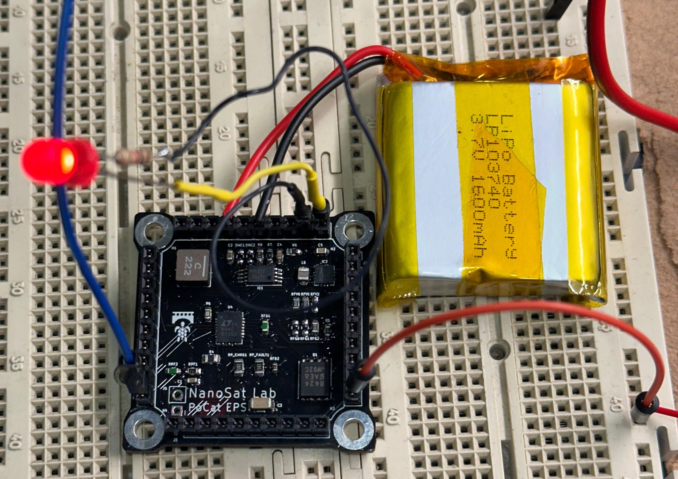
The battery selected is a 3.7 V 1400 mAh LiPo battery, with a size of 42 x 35 x 10 mm and a weight of 23.4g , and was chosen for the following reasons:
In the next table the electrical parameters of the battery are presented:
| Parameters | Value |
|---|---|
| Part Number | LP 103438 |
| Nominal Voltage | 3.7V |
| Nominal Capacity | 1400mAh |
| Internal Impedance | <60mΩ |
| Charge Voltage | 4.2V |
| Recommended Charge Current | 0.2C |
| Allowed Max Charge Current | 0.5C |
| Output Voltage Range | 2.5V - 4.2V |
| Recommend Discharge Current | 0.2C |
| Max Continuous Discharge Current | 1C |
| Pulse Discharge Current | 3C (10ms) |
| Discharge Cut-off Voltage | 2.5 ± 0.05V |
| Cycle Life to 80% Health | 500 (0.2C, 25 °C) |
Table 6: Battery electrical parameters
The battery will be enclosed within a PTFE structure, ensuring it is well-secured and protected from potential impacts during satellite operation. The enclosure is designed not only to secure the battery but also to minimize the risk of fragment release in the event of a battery explosion. It provides a containment barrier, preventing fragments from escaping and damaging other satellite components.

Figure 5: Battery PTFE structure
Also in case the battery swells due to overheating, this structure allows for slight expansion while preventing excessive swelling.
The battery also includes several features designed to prevent damage to both the battery, and to the satellite. It incorporates an IC (G3R) and a MOSFET (CJ8810) on an internal board, which provide this protection. If the voltage drops to 3.0 V, the battery will automatically disconnect protecting against overdischarge. Similarly, if the charging voltage reaches 4.28 V, it will automatically disconnect to protect against overcharging. Additionally, thanks to these components, it also offers protection against short circuits and overcurrents by temporarily cutting off the output, preventing damage to both the battery, and to the satellite
The MPPTs are responsible for maximizing the power generated by the solar cells. The STMicroelectronics SPV1040 was chosen due to it being able supports a parallel connection between the multiple solar array axes and having great efficiency. Another reason was because the manufacturer also provides simulation tools (eDesignSuite) that can be used for both dimensioning the biasing elements, as well as obtaining characteristics describing the current application. This greatly simplifies the development process and avoids potential design incompatibilities or errors.
The SPV1040 has an efficiency of up to 95% which minimizes energy losses from the solar cells, providing an output from the Energy Harvest Block between 0.3 and 5.5 V. This is critical due to the present power constraints.
Further information on the MPPT's can be found in their correspondant datasheet:
The power management IC chosen was the Analog Devices LTC4040. This component was chosen because it offers control over the battery operation and is interfaceable with the On-Board Computer through basic logic pins. Moreover, the chip also offers a few safety features, in order to prevent damage that can be inflicted by over-currents, over-voltages and temperatures exceeding our established limits.
Some other notable feautures that made the decision clear are:
The battery sensor chosen is the Analog Devices DS2782E+ it was selected due to its capacity to measure voltage, temperature and current, and estimate available capacity for rechargeable lithium-ion polymer batteries.
The voltage regulator chosen is the ISL9120IRTNZ, with up to 98% efficiency, it provides a constant output voltage of 3.3 V with a maximum current of 800mA. Since the battery produces between 3.7 V and 4.2 V, the regulator will reduce the voltage to 3.3 V, which is more energy-efficient than increasing the voltage.
A factor in the decision of selecting this part was the efficiency of the devide under the current conditions requiered by the PocketQube. The next figure ilustrates the effecinecy dependancy on consumption:

Figure 6: Voltage regulator efficiency
This regulator is also designed to prevent errors in any subsystem from impacting the battery and vice versa. It includes features such as over-temperature protection and undervoltage lockout. The over-temperature protection mechanism disables the device if the chip temperature exceeds 150°C, automatically reactivating it once the temperature falls to 115°C. Meanwhile, the undervoltage lockout function prevents the regulator from operating when the input voltage is too low, thereby ensuring the system functions correctly and safeguarding both the circuit and the battery.
The umbilical connector allows for battery charging, ans so this process is to be controlled and regulated by Texas Instruments TPS7A7002 a high-performance, positivevoltage, low-dropout (LDO) regulator. The devide was chosen due to its featuring of ultra-low dropout, useful as the input voltage through the connector is close to the charging voltage of the battery.
The hardware schematic represents the subsystem connections between components as well as all the inputs and outputs in a clear, easy to work with, manner. This section will begin with the schematic of the different blocks and components of the EPS, ending with a general view of the whole design.
The energy harvest block main compontents are the solar cells as well as the MPPTs, providing an efficient power generation block, and, to ensure the integrity and safety of these components, a Schottky diode, avoid potential power returns to the block. The MPPT connections and components schematic was generated by eDesignSuite. The next figure is the block schematic:

Figure 7: Energy Harvest Block Schematic.
Note that there is a difference bewtween the generated design and the one used. This is the change of the 6x4.7uF capacitors at the input of the MPPTs in exchange for a single 1.5uF. Observe that the only inputs are the solar panels powers and the output is the regulated voltage at around 4.4V (the battery charges at 4.2V).
The charging/discharging operations of the battery are managed and performed by the power management IC, the central piece of this subsystem block. To understand the schematic it is convenient to have clear how the main IC works:
If there is a high enough voltage (programmable) at its input, then it will output the input, while charging the battery from the same power. As the current demand on the load increases, the chip automatically decreases the battery charging current. The battery is charged through a buck regulator to step down the voltage to the selected battery charging voltage. The charging voltage can be selected using the F0,F1 and F2 pins as such:

Table 7: PM IC Control Voltages
As the satellite enters the eclipse and the voltage output by the MPPTs decreases, the chip will automatically switch to discharging the battery.
The design followed corresponds to the reference application provided by the manufacturer but set up for our necessities. The schematic is presented in the next figure and then explained: 
The voltage regulator is a buck-boost switching regulator that, in our case, will take as an input a voltage higher than the one it supplies as an output. The design chosen coincides with the typical design provided by the manufacturer, with the bypass mode deactivated, leaving the buck-boost mode on.

Figure 9: Voltage Regulator schematic
The battery sensor communicates through I2C with the OBC (SCL1,SDA1). It takes as inputs the battery poles and provides measures of it's temperatura, voltage, current and an estimation of capacity. The schematic is provided up next, guided by the manufacturers instructions:

Figure 10: Battery Sensor Schematic
The Solar Cells are located in the outer boards and interface with the lateral Picoblade connector:

Figure 11: Solar Cell Outer Board Connections Schematic.
Note that this circuit is located in the outer boards.
The killswitches remain pressed when inside the deployer and are only released when the PocketQube is ejected. While only one would be necessary two are chosen for redundancy and symmetry. They are connected to the positive pole of the battery and ensure no power is provided by it when pressed.
The schematic is provided next:

Figure 12: Killswitches Schematic.
Note that this circuit is located in the bottom board.
The umbilical connector allows for battery charging. This proccess is regulated and protected by the TPS7A7002, and the schematic follows the usual design presented by the manudacturer. It takes as an input the charging power from the connector and yields power to the battery as its only output.
The schematic is provided next:

Figure 13: Umbilical Charge Voltage Regulator Schematic.
Note that this circuit is located in the bottom board.


Figure 11: EPS PCB Schematic Overview
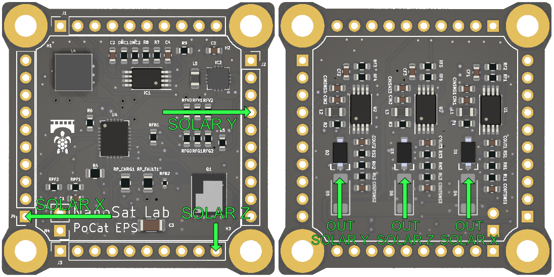
The EPS PCB is structured so that the different blocks are easily identifiable and accessible for maintenance. If we take a look at the PCB, we can see that the back Figure 12 is dedicated to the Energy Harvest Block, which contains only the MPPTs. Here, we can observe that all three MPPTs are connected in parallel, and despite they being identical, it should be easy to identify possible errors during testing. On the front Figure 12, the rest of the components are located. We can see that the part related to the Power Management IC is highlighted in red, the in battery monitor IC in blue , and the Voltage Regulator in green.

Figure 12: Views of the EPS PCB
The Energy Harvest Block is placed on the bottom layer of the PCB. Three identical blocks are placed in parallel receiving the power from the X (2 cells array), Y (2 cells array) and Z (single cell array) solar cells through the vertical connectors. The design tries to maximize compactness and cleanness in order to facilitate testing while making sure a failure in a single solar array does not become critical to the power integrity of the system.
The Power Management IC block has the main IC (LTC4040EUFD#PBF) centered on the top layer of the PCB in order to minimize the distance between the IC and the components it controls, reducing power path resistance and minimizing voltage drops. Placing the IC in the middle also helps with thermal distribution as significant heat is generated through its operation. The rest of the deisng follows standard practices to minime voltage spikes, such as the placement of decoupling capacitors to ground and so on.
The battery monitor IC and the Voltage Regulator are located as close as possible to the vertical connectors and the corner of the PCB. As the voltage regulator can generate significant heat this desicion is intended to help heat dissipation by providing more cooling space. This placement also intends to reduce thermal interference to the power management IC.
Being close to the connectors means being close to entry points of the PCB, avoiding the issues of measuring after distribution in case of the battery monitor, and the issues of power distribution for the voltage regulator.
The EPS PCB is comprised of the following layers:

Figure 13: EPS PCB Layers
The EPS software is encapsulated within the EPS task. It's main functionality is providing the OBC with battery readings on it's voltage, current generated, capacity, temperature and charging status. The task will also indicate any error generated by the Power Management IC.
The OBC is interfaced to the battery sensor through an I2C line yet it also receives and outputs information to the PM IC, as previously stated:
| Pin | Input / Output | Digital / Analog | Description |
|---|---|---|---|
| !CHRG | O | Digital | During a battery charging cycle, !CHRG is pulled low until the charge current drops below C/8 when the !CHRG pin becomes high impedance |
| !Fault | O | Digital | Indicates charge cycle fault conditions during a battery charging cycle. A temperature fault or a bad-battery fault causes this pin to be pulled low. If no fault conditions exist, the FAULT pin remains high impedance. |
| !RST | O | Digital | This pin is pulled to ground by an internal N-channel MOSFET whenever the RSTFB pin falls below 0.74V |
| CLPROG | O | Analog | VSYS Current Monitoring Pin |
| CHGOFF | I | Digital | Disable Pin for the Battery Charge. Enables the charger when tied to ground and disables it when tied to a voltage avobe 1.2V |
| !PFO | O | Digital | Pulled to ground by an internal N-channel MOSFET when the PFI input is below the falling threshold of the power-fail comparator. |
Table 1: LTC4040EUFD#PBF Interfaces with the OBC. The I/O point of reference is the EPS board.
The first duty it is responsible for is the polling of the battery sensor (DS2782E+) for voltage, current and capacity. This IC is connected to the IC2 line 1 (SCL1,SDA1).
The second duty is to keep monitoring of the state of the power harvesting and battery charging process. The LTC4040EUFD#PBF battery manager provides the required information and its acquired by directly reading GPIOs (set to input in the MCU) and an ADC in the case of the CLRPROG pin. Those PINS are the ones present in table 1.
Once all this information has been acquired by the task it is then sent to the back of a FreeRTOS queue where it will be read by the OBDH Task and subsequently stored in the flash memory.
A block diagram of the modus operandi is provided next:

Figure 1: EPS Task Data Block Diagram
The EPS consists of two main blocks. The process begins by soldering the MPPTs, and with the help of a solar simulator, they are tested using a solar cell to ensure proper functionality and that the output is as expected.
Next, the Battery Charge Block is soldered, followed by a visual inspection and continuity test to ensure there are no short circuits. Using a power supply, it is verified that the battery can provide a steady 3.3V output at the EPS output. The same test is conducted with the solar cells.
A battery charging test is performed using the solar cells to confirm that the battery charges correctly. The battery sensor is checked to ensure it reads accurate values, and the I/O pins of the Power Management IC are tested for proper operation. Finally, it is verified that the output can supply power to a load through the EPS output.
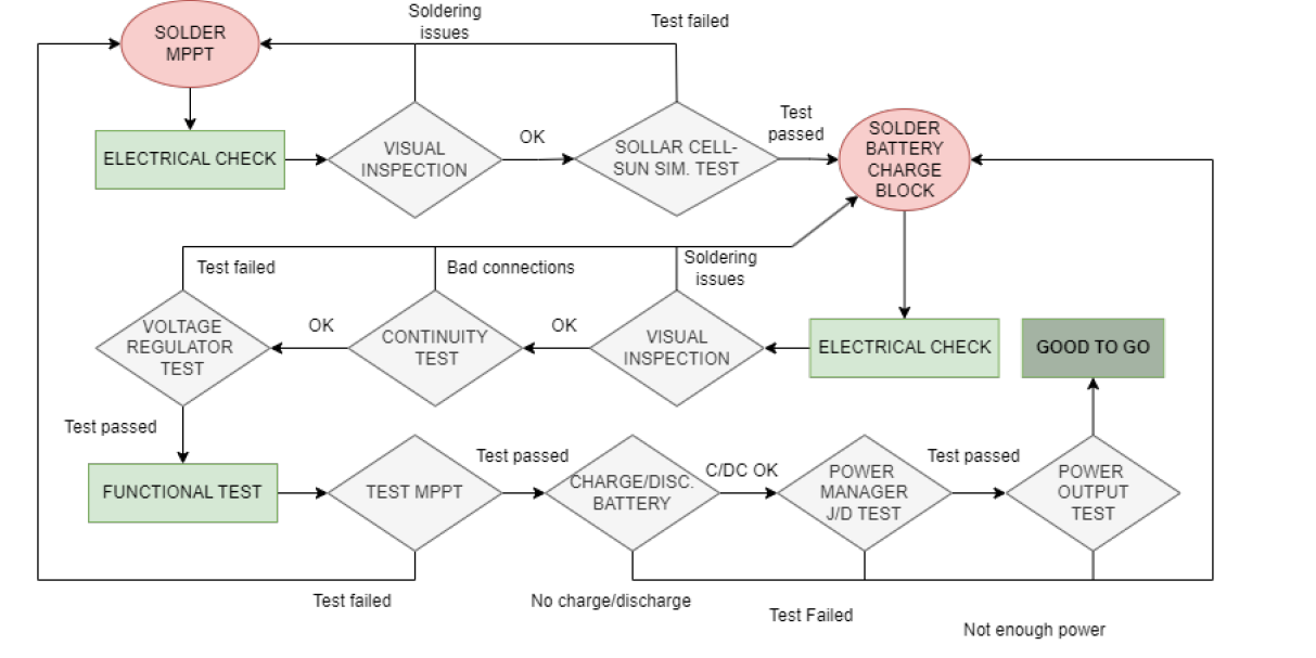
Figure 1: EPS SSV Block Diagram
The objective of these tests is to check the correct functioning of the EPS system in all its parts, to ensure correct management of the energy between the solar panels and the battery to ensure the correct management of the supply in the different subsystems.
This document is based on current but also previous versions both of hardware and software and as such be followed with care.
The objective of this test is to check all the components of the EPS board to ensure the correct connectivity of every component because solder SMD components it’s a little hard to visually analyze, for that reason we need to find some specific point that help us to ensure the connections
| Requirement ID | Description |
| EPS_reqBST00 | Check visually or with microscope some short-circuit or some pin without enough tin |
| EPS_reqBST10 | Check if all IC are orientated properly |
| EPS_reqBST20 | Check if there are continuity between (Vcc) & (GND) and (Killswith+) & (Batt-) |
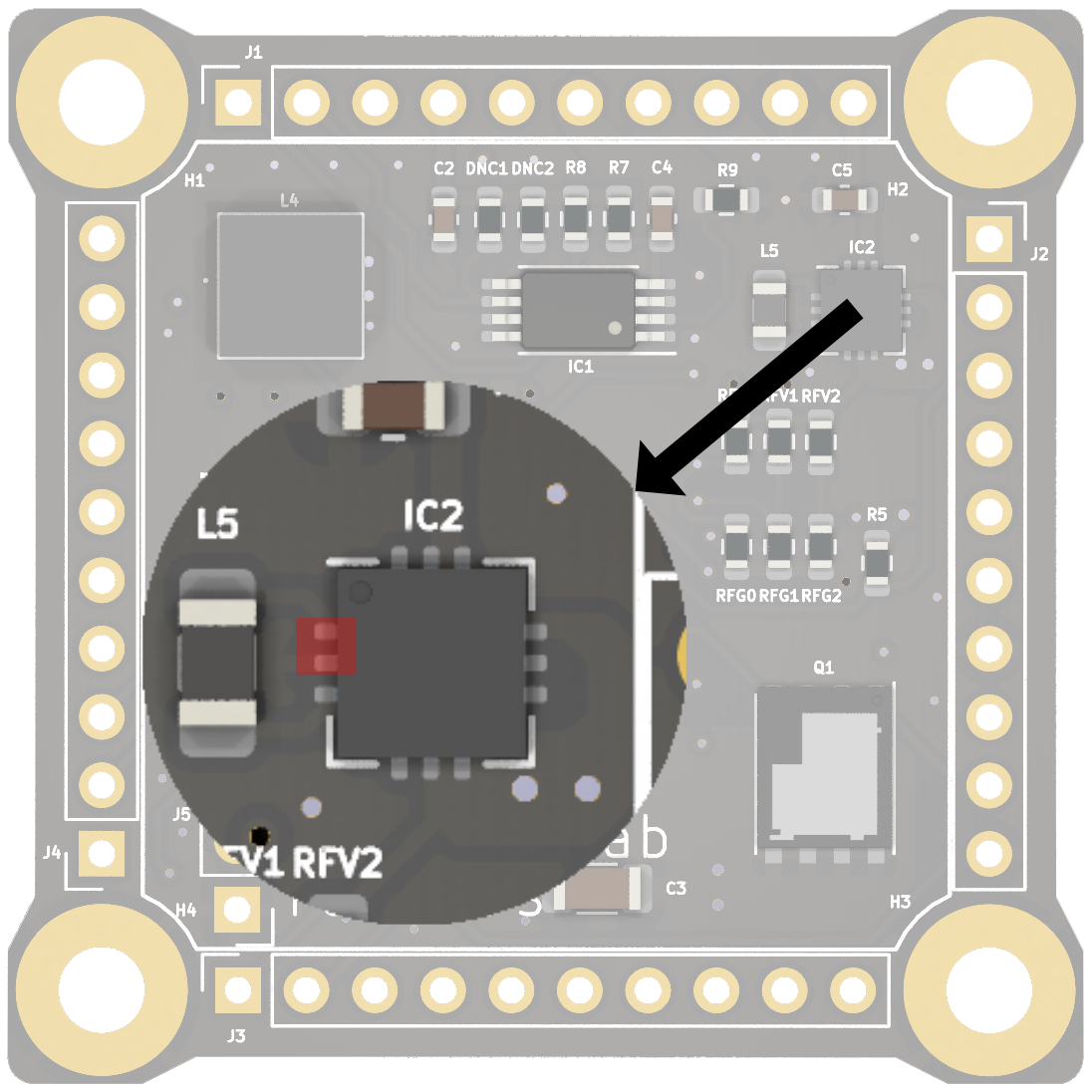
First, to verify EPS_reqBST00 and EPS_reqBT10, we need to visually inspect the components, paying particular attention to checking for potential short circuits or tin bubbles. We especially focus on U4 (LTC4040), Q1 (SIR424DP), and IC2 (ISL9120IRTNZ).
We will check the input of the MPPTs, their output, the battery power input, and the EPS output, to ensure there are no short circuits
If we encounter a short circuit during any of these checks, we should search for and repair the issue. To do this, we will return to step EPS_reqBST00 and attempt to resolve the short circuit. Pay attention to any potential tin bubbles that may have remained between the pins of the ICs
This test will be considered passed if all the requirement verifications are completed successfully
If one of the requirements fails, we cannot consider the test passed. For the following steps, where we apply voltage to the ICs, we need to ensure that there are no short circuits and no visible soldering errors to avoid damaging the PCB
| Step ID | Description | Pass/Fail Criteria | Actual | Passed\[Y/N\] |
| EPS_testBT00 | Solder all EPS board |
Ensure to solder the correct components in the correct places |
EPS components have been soldered properly | Y |
| EPS_testBT10 | Visually inspect the soldering | Check for any solder bridges between pins that could cause a short circuit or any poorly soldered pins | Some pins with short circuits were found and resolved, and some tin bubbles were removed | Y |
| EPS_testBT20 | Check electrically for short circuits | If we confirm the specified short circuits in the Test Set-Up, we pass the test | I had a short circuit in Solar Y due to the diode D2 being reversed. The diode has been rotated, and now it no longer indicates a short circuit | Y |
Two short circuits caused by tin bubbles have been cleaned on IC2 and one on the U4, which have finally been eliminated.
An error was made in the placement of a component in step EPS_testBT00, which we initially deemed as good. We overlooked the polarity detail. The diode was rotated, and with this, we can confirm that the short circuit has been eliminated.
No anomalies have been detected.
We have been able to verify that there are no short circuits in the EPS, so the first EPS board soldering test has been passed. Now, the next test will involve applying voltage, so it is important to ensure that there are no short circuits-
The purpose of this test is to verify that the EPS functions correctly electrically by powering it in different ways and checking that the outputs are as expected. Prior to this, we check for any short circuits, so now we can safely power it knowing that there are no short circuits. However, this does not mean that there are no errors, and therefore, we could potentially damage a chip. That's why it's important to have thoroughly checked the PCB in the previous test to minimize the risk of damaging any components.
| Requirement ID | Description |
| EPS_reqBT00 | Verify that we can obtain a constant 3.3V output from the EPS using a power supply |
| EPS_reqBT10 |
Verify that we can obtain a constant 3.3V output from the EPS using a battery |
| EPS_reqBT20 | Check that the MPPTs function with a power supply |
| EPS_reqBT30 | Verify that the MPPTs function with the solar cells |
| EPS_reqBT40 |
Verify that we can obtain a constant 3.3V output from the EPS using the MPPTs and the solar cells |
First, we are going to desolder diodes D4, D5, and D6 in order to separate the MPPT from the rest of the electronics.
We are going to set the power supply to 3V and limit the current to 0.1A.
To test the MPPT, we need to connect the solar cells on the top side and perform measurements on the bottom side. The GND of the solar panels must be connected to the PCB GND
Then to test EPS with the battery, it's important to connect the battery in the correct location. We must not connect the battery negative to the GND, as they are not the same. The battery negative should go to the BATT-. The output of the EPS is the 3.3V output that will be seen by the other SSVs
This test will be considered passed if all the requirement verifications are completed successfully
If one of the requirements fails, we cannot consider the test passed, as this process is important to ensure the correct power supply for the other SSVs
| Step ID | Description | Pass/Fail Criteria | Actual | Passed\[Y/N\] |
| EPS_testBT00 | Apply between 2V and 3V to the input of Solar X and check the MPPT operation | Output Solar X should have a voltage higher than the input, around 4V | The output is 4.5V, therefore we can confirm that the MPPT is functioning | Y |
| EPS_testBT10 | Apply between 2V and 3V to the input of Solar Y and check the MPPT operation | Output Solar Y should have a voltage higher than the input, around 4V | The output is 4.6V, therefore we can confirm that the MPPT is functioning | Y |
| EPS_testBT20 | Apply between 2V and 3V to the input of Solar Z and check the MPPT operation | Output Solar Z should have a voltage higher than the input, around 4V | The output is 4.6V, therefore we can confirm that the MPPT is functioning | Y |
| EPS_testBT30 | Apply 4V from the power supply to the battery input (KillSwitch + and Batt -) | Check if we have a constant 3.3V output at the EPS (VCC and GND) |
The output is not 3.3V, so the battery regulator part is not working. Additionally, there is a slight whistle coming from the EPS |
N (6.1) |
If we pass all the tests, we will resolder diodes D4, D5, and D6 to test the MPPT with the rest of the power management circuit and repeat the test to ensure the correct functioning of all EPS components with MPPT and power management together.
Now, the output pins for testing the MPPT blocks will be the EPS OUT instead the Solar OUT because we have added the diode, which makes more sense. Furthermore, we will continue using the power supply to test the battery and solar components via the EPS output
| Step ID | Description | Pass/Fail Criteria | Actual | Passed\[Y/N\] |
|
EPS_testBT40 |
Apply a voltage between 2V and 3V to the input of Solar X and check if the output works with only this power input when we illuminate it with strong light | The EPS output (VCC and GND) should provide a constant 3.3V | The EPS output provides a constant 3.3V | Y |
|
EPS_testBT50 |
Apply a voltage between 2V and 3V to the input of Solar Y and check if the output works with only this power input when we illuminate it with strong light | The EPS output (VCC and GND) should provide a constant 3.3V | The EPS output provides a constant 3.3V | Y |
|
EPS_testBT60 |
Apply a voltage between 2V and 3V to the input of Solar Z and check if the output works with only this power input when we illuminate it with strong light | The EPS output (VCC and GND) should provide a constant 3.3V | The EPS output provides a constant 3.3V | Y |
|
EPS_testBT70 |
Apply 4V from the power supply to the battery input (KillSwitch + and Batt -) | Check if we have a constant 3.3V output at the EPS (VCC and GND) | The EPS output provides a constant 3.3V | Y |
If we pass all the tests, now we will replace the power supply with solar cells and a LiPo battery. This way, we will perform the test in the real scenario
First we will connect the Lighttricity solar cells to the solar cell inputs, and then the battery (taking care with the polarity) to the pins (Killswitch+ and Batt-)
| Step ID | Description | Pass/Fail Criteria | Actual | Passed\[Y/N\] |
|
EPS_testBT80 |
We connect the Lighttricity solar cell to the Solar X input and illuminate it with strong light | The EPS output (VCC and GND) should provide a constant 3.3V | The EPS output provides a constant 3.3V | Y |
|
EPS_testBT90 |
We connect the Lighttricity solar cell to the Solar Y input and illuminate it with strong light | The EPS output (VCC and GND) should provide a constant 3.3V | The EPS output provides a constant 3.3V | Y |
|
EPS_testBT100 |
We connect the Lighttricity solar cell to the Solar Z input and illuminate it with strong light | The EPS output (VCC and GND) should provide a constant 3.3V | The EPS output provides a constant 3.3V | Y |
|
EPS_testBT110 |
Connect the LiPo battery to the battery input | Check if we have a constant 3.3V output at the EPS (VCC and GND) | The EPS output provides a constant 3.3V | Y |
|
EPS_testBT120 |
Connect a solar cell illuminated with strong light, and also connect the battery at the same time | Check that the output of the EPS remains at a constant 3.3V even when it receives sufficient energy from both inputs (solar and battery) | The EPS output provides a constant 3.3V | Y |
In this example, we can observe that when we connect a small load like an LED to the EPS output, the LED lights up when we illuminate the solar cell with a strong light, in this case from a headlamp

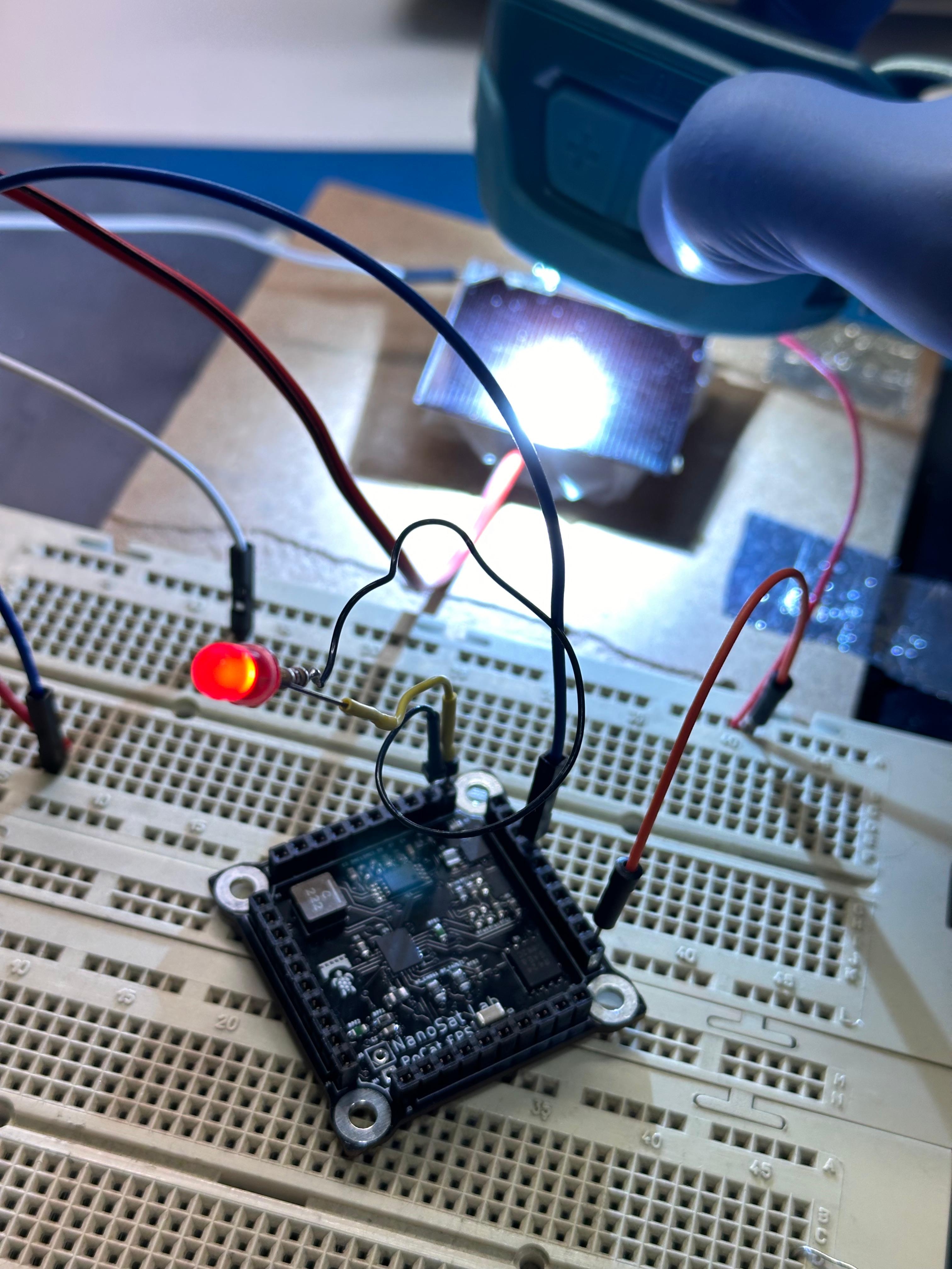
We can also see the result when connecting the LiPo battery.
We can confirm that we are able to provide a constant voltage of 3.3V at the output of the EPS using both the solar cells and the battery. Therefore, we will be able to properly power the different SSV either by solar light or by battery
After checking that supplying 4V from the power supply to the EPS via the battery pins does not provide the expected constant 3.3V output, and additionally hearing a slight whistle from the PCB, we will review the PCB once more to identify any possible overlooked issues or visual signals that may provide clues.
We observe that the LX2 (1) and PGND (2) pins of the ISL9120IR regulator are short-circuited, so we proceed to remove the short circuit.
| Step ID | Description | Pass/Fail Criteria | Actual | Passed\[Y/N\] |
| EPS_testBT30 | Apply 4V from the power supply to the battery input (KillSwitch + and Batt -) | Check if we have a constant 3.3V output at the EPS (VCC and GND) | The output is a constant 3.3V. | Y |
If we illuminate the solar cells with classroom lighting or the flash of a mobile phone, we observe that the solar cell reaches 2V but is unable to activate the MPPT, thus it does not function. We require a more powerful light source, such as a headlamp, which also generates 2V from the solar cell but provides more current. So, we should not depend solely on the voltage reading from the solar cells to determine their operational status
Now, we have the MPPT working with the Lighttricity cells and the battery regulator as well. Therefore, we can now proceed with the next tests, as we can confirm that the generated voltages are correct.
The objective of this test is to check the correct functioning of battery sensor that provides to OBC some data about the battery like the Voltage, Current and Temperature.
| Requirement ID | Description |
| EPS_reqBS00 | Be able to read the battery voltage |
| EPS_reqBS10 | Be able to read the temperature of the battery using NTC |
| EPS_reqBS20 | Be able to read the actual current value |
| EPS_reqBS30 | Be able to read the average current value of the last 28s |
| EPS_reqBS40 | Be able to read the accumulated current value |
First, we will connect the EPS board to the STM32 Nucleo via I2C connection, and then connect the Nucleo to the STM32CubeIDE software.
Then we connect the NTC temperature sensor on EPS board, to modify the temperature we can use a Peltier cell that if we invert polarity will give us hot or cold as we need
Into the battery connector, we can connect a real LiPo battery or power supply.
The last is connect some kind of thermometer that gives us a real measurement of the read temperature of NTC sensor to compare with it.
This test will be considered passed if all of the following actions are performed successfully:
On Standby
# Tests as Run (Legacy)1. Test description and objectives
The purpose of this title is to verify the effective communication with the internal blocks of the EPS board and the OBC. This communication will be carried out using the I2C bus. The test is specifically aimed at reading the values of registers containing crucial data such as temperature, voltage, current and battery state of charge. To perform the test we will first use as OBC the STM32 board that we will use to read the registers of each chip separately and
For this test, I utilized the STM32 board, the core-476RGD, with the aim of measuring the temperature through readings from the DS2782E+ chip via I2C communication. These measurements will be carried out by the OBC to monitor the system's temperature, ensuring the battery does not enter a charging state when it exceeds 45 degrees Celsius or when it falls below 0 degrees Celsius. In such cases, it can be hazardous as the battery may explode if it's in a charging state.
The following materials were used:
Below, I present the board and the necessary connections for temperature readings:
Since the temperature must be between 0 and 45 degrees Celsius, under normal conditions, it's logical for it to be around 24 to 26 degrees Celsius. 13- Test Plan In this case, the EPS board is powered directly by the 3.3V supply from the STM32. To measure the temperature, we need to read registers 0x0A and 0x0B, the former for the most significant bits and the latter for the least significant bits. Each unit measured in this register represents 0.125 degrees Celsius. Below is an image representing the two registers to read, directly extracted from the DS2782 datasheet:
The code used is as follows:
Satisfactory results were obtained, with temperature readings ranging from 23.25 ºC to approximately 29 ºC in multiple iterations. These values fall within the expected range. To ensure that the value varied with exposure to temperature changes, I conducted an experiment by, for example, placing the fingertip (previously discharged from static electricity), and the changes were gradual, with the temperature gradually increasing with each iteration of the I2C register read function. (The values for this test point were considered as floats).
An example of execution was as follows; after placing the fingertip, changes in the read value were observed:
No anomalies were found.
I must sieve and pass an integer instead of a float because transmitting that information to the OBC is more complicated using floats, and relevant information is lost. Therefore, based on the results, it is concluded that the DS2782E+ chip accurately measures temperature.
Voltage of the battery measurement - DS2782E+
1- Test Description and Objectives
Measuring the voltage is pivotal for understanding the battery's charge status, preventing overcharging or deep discharge, predicting battery life, and optimizing overall system performance by ensuring safe operations and maximizing battery lifespan.
2 - Requirements Verification
3 - Test Set-Up
The following materials were used:
4 - Pass/Fail Criteria
According to the battery specifications and the voltage from the solar cells, the voltage range supported by the battery is from 0 to 4.25V with a maximum of 1A. The solar cells provide between 3.7V and 4.2V, fitting well within the correct voltage range. Regarding the current, at the SPV1040 output, there's an average of 250mA that can vary depending on the Maximum Power Point Tracking (MPPT), adjusting to the energy values received from the solar cells to maximize the power output.
5 - Test Plan
Code:
Running this function in the main.c while having Putty connected to COM3 port at a bus speed of 115200 bits/s will display the battery terminal voltage on the screen.
The registers that I measured are the next:
6 - Test Results
I've obtained an average result of 3.85 V. At times, it dropped to 3.7 V, but it never exceeded 4 V.
7 - Anomalies
No anomalies was found
8 - Conclusions
The voltage values measured at the battery terminals are correct as they fall within the typical operating range.
Current measurement - DS2782E+
1 - Test Description and Objectives
The objective of this test is to determine the current flowing through the battery using a 330-ohm resistor in the circuit, connected between Vcc and GND on the EPS board. This will allow us to assess how the battery discharges and verify if the current values do not exceed the allowed limit of 1 A. This type of measurement allows assessing the battery's charging and discharging efficiency while identifying potential anomalies in the energy flow. This is crucial to ensure optimal performance and safe management of the battery within the system.
2 - Requirements Verification
3 - Test Set-Up
Materials:
The following materials were used:
We use the same setup as in the previous test, but this time placing a 330-ohm resistor between the Vcc and GND pins of the EPS board, which can be seen in this image:
4- Pass/Fail Criteria
According to the battery specifications, the current flowing through it should not exceed 1A; typically, we obtain values around 100 to 150 mA. When using a 330-ohm resistor, it's expected to yield readings around 10 mA. By verifying this, we can conclude that the measurement is accurate and acceptable within the electrical specifications of the devices involved.
5- Test Plan
With the configuration previously set up in the voltage test, connecting the battery to the EPS board and, in turn, to the NUCLEO-L476RG using I2C communication as in the previous cases, we can carry out the reading of the current registers.
Add the code that I wrote to read the registers that contain the current information. That registers are the next:
Code:
6- Test Results
The obtained result is 11.87 mA when a 330 Ohm resistor is connected between Vcc and GND.
7- Anomalies
Not found any anomalies
8- Conclusions
The result is as expected. In summary, we have successfully measured the discharge current flowing from the battery through the resistor. We can differentiate between input and output current based on whether the battery is charging or discharging, which is reflected in the sign of the measured value.
State of Charge of the battery measurement - DS2782E+
1 - Test Description and Objectives
This test aims to assess the accuracy and reliability of the State of Charge (SOC) measurement conducted by the DS2782E+ chip within the battery system. The objective is to verify whether the SOC readings align with the expected charge levels of the battery during various charging and discharging scenarios.
2 - Requirements Verification
3 - Test Set-Up
Materials:
The following materials were used:
We use the same setup as in the current measurement case. Here, our connections will be similar, with the battery logically connected with the positive terminal at the kill switch and the negative terminal at BATT-.
4- Pass/Fail Criteria
Ensure that the battery capacity reading does not exceed the specified limits of 1400mAh. It should accurately represent the actual capacity and align with calculations derived from the SOC (State of Charge) and RARC (Remaining Standby Absolute Capacity Register Format).
5- Test Plan
Through the I2C code for register reading, we retrieve the RARC register, which provides us with the value directly. Here's the code attached:
In the last image I used the next method to calculate the SOC:
The Vmax = 4.2 V and Vmin = 3.7 V for our battery.
Since it's not feasible to calculate the SOC value in a single iteration, it's necessary to conduct multiple iterations, progressively increasing the value until it stabilizes.
6- Test Results
I have obtained a basic approximation of the State Of Charge using voltage measurement. However, this is not the only method to calculate it. Since I do not have SOC curves for the exact battery model and the capacity obtained through RARC does not give any value other than 0, I have opted for this method. In the last realization of this test, I could see how the battery's state of charge was at 27.17% and was decreasing to values of 26 and 25 as it discharged. I could verify its discharge by connecting a 330 Ohm resistor to the system's output and the current showed negative
7- Anomalies
"It gives a value of '0' through Putty when calling its function within the while loop.
8- Conclusions
It's necessary obtain a SOC curve to accurate the result and use another method that implicate the temperature or the current also.
4.5.9.2 - TEST 2 - Solar cells measurement
1. Test description and objectives
The objective of this test is verify that the solar cells generate the expected electric current under different solar illumination conditions. We will use the EPS connected to the STM32 board and the latter connected to the PC. We will read the voltage measured at the output of the system and we will also perform the manual measurement using a voltage and current tester to verify what voltage is read at the output of: the solar cells, each of the SPV1040 and then the output of the voltage regulator to verify if the 3.3 V supply is reached under maximum incidence of sunlight.
2. Test requirements
Material:
3 - Test Plan
4 - Test Results
With light exposure (in this case, I did not use sunlight), I have obtained values of 1.81 V at the terminals of the solar cell, and it has remained at the input of the SPV1040, when in reality, the voltage should increase to 3.5 V. Measuring with the tester, there is isolation between the different circuits that come from each SPV1040. However, it doesn't seem that the MPPT is working properly.
5 - Anomalies
The SPV1040 not work correctly, because the value of the out voltage is not increased respectively than the enter voltage from the cells.
6 - Conclusions
Could be necessary revise the connections of the circuit.
TEST 3 - Charge/Discharge of the battery
1. Test description and objectives
Charge and discharge the battery until its capacity is reduced to a minimum and observe how many charge and discharge cycles the battery can withstand before its total degradation. The objective is to verify how many charge and discharge cycles the battery can withstand.
2. Test requirements
3. Results
The test was performed in summer of 2023 with favorable results.
Finish of the test plan of 2023-2
-------------------------------------------------------------------------------------------------------------------------------------------------------------------------------------------------
The test for the EPS PCB has been done during the 03/05/2023.
The test passed the visual inspection since the outer physical checking was successful.
The pins', passive and active components' connectivity were successfully accomplished considering that there were no open ends or shorts, and the component values were correct.
The in-circuit testing was passed since the connections between all of the components and pints of the PCB were verified.
During the examination of the PCB for potential short circuits, it were identified three of them. In order to rectify this issue, the affected components were re-soldered and a new test was made to confirm that the problem had been successfully resolved.
The PCB passed the electrical test and is ready to do more complex tests.
The objective of this test is to verify that when providing the PCB with the power supply, the voltages and currents are correct on the whole PCB
The voltages required for each component are summarized in the following chart (they can be seen from the datasheet of each component):
| COMPONENT | Vin Min (V) | Vin Max (V) | Vo Min (V) | Vo Max(V) |
| SPV1040TTR | 0.3 | 5.5 | 2 | 5.2 |
| LTC4040EUFD#PBF | 3.5 | 5.5 | 3.5 | 5 |
| ISL9120IRTNZ | 1.8 | 5.5 | 1 | 5.2 |
| DS2782E+ | 2.5 | 4.5 | - | - |
This test will be verified if the voltage obtained in the measurements of each component of the PCB is between the expected values.

This test for the EPS PCB has been done during the 22/05/2023.
The test has been correctly passed, since the different measures correspond to the correct values.
No anomalies has been detected
The PCB passed the test and is ready to do more complex tests.
The aim of this test is to verify that the voltage regulator can maintain a constant 3.3V level regardless the input value.
| Requirement ID | Description |
|---|---|
| EPS - 01 | It is necessary that the output of the PCB is a constant voltage of 3.3V |
These blocks will be verified if the output of the charge / discharge block is the battery voltage and the output of the voltage regulator is a constant voltage of 3.3V


This test for the EPS PCB has been done during the 22/05/2023.
When the chout pin was checked it had the 3.3V of the battery input
Doing the step 8 the following chart is obtained:
| VCC | 2V | 2.5V | 3V | 3.5V | 4V |
|---|---|---|---|---|---|
| Vin | 3.26V | 3.27V | 3.27V | 3.26V | 3.26V |
As it can be seen, the voltage regulator always gives the expected 3.3V.
Since the two requirements verification has been accomplished, the EPS PCB can pass to the next test.
No anomalies has been detected
The PCB passed the test.
The objective of this test is to simulate various conditions that can occur in the PCB in order to verify the proper functioning of the charge / discharge block.
| Requirement ID | Description |
|---|---|
| EPS - 11 | When only the battery input is connected, the output of the charge / discharge block must be the battery input voltage |
| EPS - 12 | When a voltage is applied to the output of the harvest block, the output of the charge / discharge block has to be the harvest block input, and the battery input must be disconnected. |
| EPS - 13 | When the temperature is above 40 ºC, the battery input must be disconnected |
The test will be successfully completed if all the requirements are met.
When the chout pin was checked it had the 3.3V of the battery input
When the input connected was the Solar_Y pin, the voltage measured was 4.68V
When both power supplies were connected, the voltage read was 4.68V and the display of the power supplies showed the next values (the right one is connected to Solar_Y)
No anomalies has been detected
The PCB passed the test.
The objective of this test is to simulate the different combinations of the solar cells illuminated to verify that it can supply the 3.3V needed.
It is necessary that the output voltage of the energy harvest block, when at least one of the solar cells is active, is at least 3.3V
With all the combinations of active solar cells tried, the voltage at the output of the energy harvest block has been proved to always have a level of around 4.68V
No anomaly was detected.
The payload has passed the test
The aim of this test is to verify that the battery sensor situated in the PCB works properly and that it can communicate with the computer using the I2C protocol.
| Requirement ID | Description |
|---|---|
| Sensor correctly supplied | Check again that the pins in charge of the supply of the sensor receive the necessary 3.3V. |
| I2C Connection | It is necessary that the battery sensor can communicate correctly using the I2C pins |
| Correct lectures | The output values of the battery sensor (temperature, voltage and current), shown in the PC, has to correspond to the expected ones (temperature is the easiest to check, since it can be compared with a thermocouple ). |
The battery sensor will be verified if the requirements mentioned before are fulfilled. If in one of them it is detected any anomaly it will have to be corrected, otherwise the board can not pass to the other tests.

The first thing that it is necessary to look at is the i2c protocol employed by the DS2782E+. This information is shown in the page 26 of its datasheet.
 In this image the protocol is resumed.
It can be seen that the first thing to do is send a start bit, followed by the slave device address and a write bit. The device will acknowledge the communication with an ACK signal. Upon the receipt of the ACK, confirming a successful connection with the device, it is send the memory address from which we want to read, and the device will respond with another ACK.
With the previous steps done, another start bit is transmitted, followed by the the slave device address and a read bit. The DS2782E will respond with an ACK and proceed to provide the data from the memory address previously specified.
To conclude the communication, a non-acknowledgment (NACK) signal is transmitted, followed by a step bit.
Another crucial aspect to consider is the addresses requiered to communicate with each sensor. This addresses are specified in the page 23 of the DS2782E datasheet:
DS2782E slave Address: 0x34 (HEX)
Temperature register: 0A (HEX)
Remaining Active Absolute Capacity register: 0x02 (HEX)
Voltage register: 0C (HEX)
Current register: 0E (HEX)
It is also important to know the frequency that is needed in order to do a proper communication with the DS2782E. This is shown in page 3 of the datasheet.

Taking all of this into account, a possible code implementation is the following one:

When trying to make the communication with the sensor, no response was obtained. To solve this problem the following steps where followed:
1. Verify the connections
All the I2C connections are well connected with the corresponding PINS, and the 3.3V are detected in the input pin (killswitch).
2. Check the components
The components connected are the corresponding ones and in the correct positions according to the Ki-Cad schematic. It is also important to check that no component has any short circuit.
3. Verify the addresses of the device
The device address is the correct one (0x34). It can be seen in the I2C Addresses document of the nanosatlab wiki or in the datasheet of the device
5. Use the oscilloscope to check the I2C bus to see which is the problem
When checking the signal with the oscilloscope, the signal of the clock was not clear and it made strange changes. To try to solve this problem, the intern pull-up resistance of the nucleo-boared where disconnected and they where placed in a protoboard with a value of 20K Ohms.

With that done the signal was checked again using the oscilloscope and, as it can bee seen in the following image, the SCL signal was working properly.

The next thing to be checked was that the message from the nucleo-board was well send and with the correct value (the address of the battery sensor). To do that, the oscilloscope was connected to the SDA pin and the signal from the following image was shown. The value send is "1101000" (0x34), followed by the write bit.

Once the nucleo-board I2C transmission was working as expected, it was time to connect the nucleo-board to the EPS board, removing first the pull-up resistances of the protoboard and checking that the ones placed in the EPS were also the 20K ohms ones.
Looking again the signals in the oscilloscope, it can bee seen that the EPS battery sensor was responding with the temperature value that was asked.

To make sure that this value was real, the board was heated with the hot air blower, and the temperature given by the EPS was compared with the temperature given by a thermocoupler. The following images shown the test set up
Two figures are now shown comparing the values of temperature:

EPS value: 00011110 (30º)
Thermocoupler value: 28º

EPS value: 00111110 (62º)
Thermocoupler value: 64º
It can be concluded that the temperature given by the temperature sensor of the EPS is correct.
The test for the EPS battery sensor has been done during the 01/06/2023.
The test has been passed successfully, since the communication with the battery sensor was done and the values are correct.
The anomalies detected during this test are explained with detail in 6.5.2.
The PCB passed the I2C test and is ready to do more complex tests.
The aim of this test is to verify that the ADCS board can be powered with the EPS board.
| Requirement ID | Description |
|---|---|
| Input Power | It is required to check that the intput pin of the ADCS when it is connected to the EPS output is 3.3V |
| Sensor reading | It is necessary to be able to read from a sensor of the gyroscope using I2C |
The PCB will be verified if the input power of the ADCS when it is connected to the EPS is 3.3V and it is possible to read from the gyroscope sensor.
The test for the EPS PCB has been done during the 02/06/2023.
The input of the ADCS when connected with the EPS is the expected 3.3V.
The following two images show the test set-up and the recieved values of the gyroscope

No anomalies has been detected
The EPS can supply successfully the ADCS board and the data from the gyroscope can be read. Therefore, the EPS has passed this test.
# Communications (COMMS) # Subsystem DescriptionThe communications subsystem is responsible for telecommand reception and telemetry transmission. Being so that the functionality of the satellite's control from the Earth ground station completely relies on the COMMS subsystem. Therefore, it is imperative for the COMMS subsystem to fulfill specific requirements to facilitate accurate communication and seamless operation of the satellite.
It is opted for the utilization of LPWANs (Low Power Wide Area Networks), specifically employing the LoRa (Long Range) physical layer technology. COMMS hardware is located both in the OBC-COMMS board as well as in a lateral board (where the antenna is soldered or screwed). The subsystem can be divided into different blocks to identify their functionality.
The first one is the power circuit, tasked with ensuring the proper power supply and composed by passive components. The transciever is the key component of the SS, responsible of both the recepction as well as the transmission of information from and to the ground station. It communicates with the MCU through SPI, as a slave, and performs signal modulation and demodulation.
The transciever requires an stable reference signal in order to perform its tasks, this is provided by a crystal oscillator.
The RX Line transmits the received signal from the antenna to the transciever. The line is balanced by a balun and impendance matched. The TX Line transmits the transmitted signal from the transciever to the antenna and presents different filters and matchings. The line to be used at each instant is selected by the switch, controlled by the transciever, which is at the same time controlled by the MCU.
Finally, the antenna, connected to the switch through a line that boths filters and matches impedance, is responsible for physically receiving and transmitting electromagnetic waves.

Figure 1: COMMS Functional Architecture Block Diagram
| Subsystem | ID | Requirement |
|---|---|---|
| COMMS | COMMS - 0000 | The Communications Subsystem (COMMS) shall work in the ISM band via radio links. |
| COMMS | COMMS - 0010 | The COMMS subsystem must transmit at a maximum power of 20 dBm. |
| COMMS | COMMS - 0020 | The COMMS subsystem must support half-duplex communication, enabling both transmission and reception of data. |
| COMMS | COMMS - 0030 | Be able to deploy the omnidirectional quarter wavelength antenna once the satellite is deployed in space. |
| COMMS | COMMS - 0040 | The COMMS shall periodically transmit the telemetry of the spacecraft. |
| COMMS | COMMS - 0050 | All packets shall be tagged with a timestamp. |
| COMMS | COMMS - 0060 | The COMMS must be able to receive Telecommands from the ground segment and send a reception acknowledgement. |
| COMMS | COMMS - 0070 | The COMMS shall have the capability to provide past telemetry housekeeping. |
| COMMS | COMMS - 0080 | The transmitted beacon shall contain a subset of information from the whole satellite housekeeping. |
| COMMS | COMMS - 0090 | OBC and COMMS subsystems must communicate through SPI. |
| COMMS | COMMS - 0100 | The S/C shall be capable of changing the operating frequency using a telecommand. |
| COMMS | COMMS - 0110 | The satellite must comply with European regulations. |
| COMMS | COMMS - 0120 | Be able to distinguish between wanted packets and unwanted packets. |
Up next is provided a table including the most important components of the COMMS subsystem. In the following sections is found information about each one of them as well as the overall design of the system.
| Specification | Value |
|---|---|
| Frequency | 868 MHz |
| Modulation | LoRa |
| Bandwidth | 125 kHz |
| Maximum output power | 22 dBm |
| Maximum current consumption | 118 mA |
| Effective data rate | 537.1 bps |
| Coding rate | 4/5 |
| Spreading Factor | 11 |
| Antenna | λ/4 monopole |
Table 1: COMMS Quick Facts Table
It is crucial to consider that the restricted size of the PocketQube will dictate the maximum power of the signal to can transmit. This is both due to the physical space constraints, discarding the possibility of more complex designs and also due to the power constraits of having a small surface area on the lateral boards for energy gathering.
Hence, it requiered to employ technlogies that provide low consumption, small amounts of space as well as the necessary power and range capabilities to meet the mission's requirements.
It is opted for the utilization of LPWANs (Low Power Wide Area Networks), specifically employing the LoRa (Long Range) physical layer technology. The selected transciever for the subsystem is the SX1262 LoRa Transciever from Semtech, chosen from a range of options due to its superior output, frequency and lower power consumption in comparison to its counterparts:
| Chip | SX1262 | SX1261 | SX1268 | SX1272 | SX1276 | SX1278 |
| Physical Layer Technology | LoRa | LoRa | LoRa | LoRa | LoRa | LoRa |
| Frequency range | 150 - 960 MHz | 150 - 960 MHz | 410-810 MHz | 860-1020 MHz | 137-1020 MHz | 137-525 MHz |
| Bandwidth | 7,8 - 500 kHz | 7,8 - 500 kHz | 7,8 - 500 kHz | 7,8 - 500 kHz | 7,8 - 500 kHz | 7,8 - 500 kHz |
| Maximum output power | 22 dBm | 15 dBm | 22 dBm | 20 dBm | 20 dBm | 20 dBm |
| Maximum current consumption | 118 mA | 25,5 mA | 107 mA | 125 mA | 120 mA | 120 mA |
| Size | 4mm x 4mm | 4mm x 4mm | 4 mm x 4 mm | 6 mm x 6 mm | 6 mm x 6 mm | 6 mm x 6 mm |
Another factor taken account into the desing choice is the flight heritage of the technlogy as FOSSASAT-1 already practically demonstrated the feasibility LoRa communications in space.
The switch to be used must fulfill certain requisites established mainly by the transciever. First of all it is important to consider the frequency ranges it'll have to work on, being around 868 MHz in our case. Furthermore the switch is to be controlled by an analogic pin of the SX1262, therefore it must work at voltages as close as possible as 3.3V. The insertion losses are also an important factor, having to be minimized. The commutation control scheme has some flexibility as software can be defined to sort out path chosing.
The switch selected is the BGS12P2L6E6327XTSA1 from Infineon. Previously the BGS12PL6E6327XTSA1 was used but due to availability issues the first one has been selected. The new switch boasts less losses while being feature in the same package as the old one. Both provide low current consumption and fulfill the previous requirements.
The COMMS crystal oscillator is responsible for providing a stable RF reference signal to the transciever. This signal is to be of a frequency of 32 MHz as established by the transciever manufacturer. It is mandatory that the selected oscillator remains stable enough in a range of temperatures around -20ºC-80ºC.
The selected crystal oscillator is the FA-128_32.0000MF20X-K5 from EPSON due to it's size and appropiate frequency drifts in the temperature ranges expected. This oscillator is also recommended by the transciever manifacturer.
The selected antenna connector is the D.FL75-R-SMT-1(40) from Hirose Electric due to it fitting the frequency and thermic requirements as well as being easily mated.
The antenna is the part of the communications system that radiates the signals towards the ground station and receives the signals coming from it. There are different kinds of antennas, but not all of them fit the needs and constraints of a PocketQube mission. Derived from the requirements, the antenna needs to have the following features:
Having analyzed the different alternatives of antennas, only wire antennas accomplish the size requirements while keeping an easy method to fold them. A monopole antenna is selected due to the complications that arise from using a dipole design (possible interferences and modification of some features of the radiation pattern) as well as the simplicity to fold it.
Note that an ideal monopole has an infinite ground plane that, following the image theory for currents, will radiate as if the monopole had another symmetric element on the other side of the ground plane. However, in real life, the ground is neither a perfect conductor which cancels the radiation in the horizontal direction, nor it has an infinite ground plane, which generates some back lobes.
The antenna designed then is a piece of metric tape cut at a lenght of around λ/4 (the frequency being 868MHz). This materials used in these tapes provide proper transmission and reception of EM raditation in our desired frequency range while being resilient to radiation in other parts of the spectrum. It is also a cost-effective solution as well as a proven through flight heritage deisgn. Despite the fact that the length of an ideal monopole is a quarter of the wavelength (λ/4 = c/4f = 3·10^8/4·868·10^6 = 8.64 cm) depending on the characteristics of the antenna and where it is placed, this length can differ a bit.
To tune the antenna it was connected to a VNA and then cut until the peak was placed at 868 MHz. The obtained length was 9.5 cm, also counting the part of the antenna that is inside the PocketQube.
Another important test to determine the gain (or loss) of the antenna and the direction of radiation is the measurement of the radiation pattern. This was done in the anechoic chamber of the department of Signal Theory and Communications. Next a picture of the anechoic chamber is shown, and the follwoing figures provide the results of the radiation pattern.

Figures: UPC anechoic chamber & Normalized radiation pattern

Figure: XY YZ ZX cuts of the normalized RPE
The maximum gain obtained in our case is 1.15 dB, and the directivity is 3.115 dB. The θ−3dB is approximately 60º. Finally, the next figure presents the gain radiation pattern.

Figure: Gain radiation pattern in dB
The overall design, separated by functional blocks is provided next:

Figure 1: COMMS Colored Schematic. Note that the switch used in this schematic corresponds to the previous version, but no functional changes are presented.
Note that the schematic for the OSC is provided in Figure 4. The 3V3_PERM line arrives through the vertical connectors, from the EPS. Some component value choices justification are provided in the next section (PCB Design), but it can be said that most of them follow the reference design at our selected configuration.
The SX1262 allows different set-ups for power distribution, interupt handling, clock reference signals and switch control. The selected power distribution (power circuit) uses a DC-DC regulator, reducing the power consumption of the core. A reference schematic from the manufacturer is provided next:

Figure 2: SX1262 DC-DC Power Configuration Schematic
While the SX1262 might be provided of a reference signal by a TCXO (Temperature Compensated Crystal Oscillator) our design involves the use of an on-chip oscillator (OSC). Leaving the DIO3 (PIN 6) unused. The communication between the MCU and the transciever is performed through SPI (PINS 16 to 19) and the DIO 1 line is used to transmit interruption to the OBC.
A table of the function and ID of each PIN of the transciever is provided next:
| Pin Number | Pin Name | Type (I = Input, O = Output) | Description |
|---|---|---|---|
| 0 | GND | - | Exposed Ground pad |
| 1 | VDD_IN | I | Input voltage for power amplifier regulator, connected to pin 10 |
| 2 | GND | - | Ground |
| 3 | XTA | - | Crystal oscillator connection, can be used to input external reference clock |
| 4 | XTB | - | Crystal oscillator connection |
| 5 | GND | - | Ground |
| 6 | DIO3 | I/O | Multi-purpose digital I/O - external TCXO supply voltage (NOT USED) |
| 7 | VREG | O | Regulated output voltage from the internal regulator DC-DC |
| 8 | GND | - | Ground |
| 9 | DCC_SW | O | DC-DC Switcher Output |
| 10 | VBAT | I | Supply for the RFIC |
| 11 | VBAT_IO | I | Supply for the Digital I/O interface pins (except DIO3) |
| 12 | DIO2 | O | RF Switch control |
| 13 | DIO1 | O | Interrupt Output to the MCU |
| 14 | BUSY | O | Busy indicator |
| 15 | NRESET | I | Reset signal, active low |
| 16 | MISO | O | SPI slave output |
| 17 | MOSI | I | SPI slave input |
| 18 | SCK | I | SPI clock |
| 19 | NSS | I | SPI Slave Select |
| 20 | GND | - | Ground |
| 21 | RFI_P | I | RF receiver input |
| 22 | RFI_N | I | RF receiver input |
| 23 | RFO | O | RF transmitter output ( high power PA) |
| 24 | VR_PA | - | Regulated power amplifier supply |
Table 1: SX1262 PIN Layout and description
Physically those PINs relate to the following layout in the SX1262:

Figure 3: PIN Layout from the SX1262 top view
The trimming capacitors on the clock may not be connected depending on the clock selection, if it is to be changed. As a matter of fact the transciever offers the possibility of configuring the capacitance of internal capacitors to perform the same task as this ones. On current PoCat design they remain not connected.

Figure 4: Crystal Oscillator Schematic
The switch is controlled through the DIO2 (PIN 12) of the SX1262, selecting the RF2 path (transmission line) when the pin rises to high. If it drops, the path selected will then be the RF1 (reception line). It is supplied with 3.3V through the vertical connectors.

Figure 3: Switch Schematic
The rest of the design follows the reference schematic provided by Semtech on the SX1262 for usual applications with some changes to optimize space and provide testing capabilities, such as the inclussion of a test probe in the transmission line.
The upper part of the connection between the transceiver and the switch transmits the signal generated in the SX1262 (RFO line), then it is amplified (VR PA line) and the harmonics of second and higher order are filtered. The bottom lines are the ones that take the signal received from the switch to the transceiver. As the transceiver needs a balanced signal and the switch provides an unbalanced one, a balun is added in between to do the unbalanced-balanced conversion. One last important aspect is that all the circuits that connect the main components (transceiver-switch-connector) are matched to 50 Ω.

The COMMS PCB must support the schematic presented before with a design that minimized losses and interferences. Its tasks correspond to those stablished in the functional description of the system, mainly providing TT&C (Telemetry Tracking an Command) capabilities, as well as P/L data acquisition.
The COMMS subsystem is encapsulated within the OBC-COMMS PCB, sharing space in the same board. In this section the COMMS related lines and components will be explained while the OBC ones remain in their section.
It is interfaced, like the other PCB's in the stack, with the rest of the boards through vertical connectors on each side. Despite this the only relevant inter-board connections in the COMMS case are both the ground plane and voltage line as well as the antenna itself. The later is communicated through a coaxial connector, one in this PCB and another in a lateral board where the antenna is soldered or screwed.
The PCB has 4 internal layers distributed as shown in the next figure:

Figure 4: OBC-COMMS PCB Structure
An explanation of the layer distribution is provided next:

Figure 4: OBC-COMMS PCB With colored blocks
The power circuit uses the following components:
These two capacitors reduce noise to the input voltage of the transciver and avoid undesired voltage peaks.
| Temp. coeff. or Cap. Change | Temp. Range | Ref. Temp. | Rated Voltage | Capacitance | Capacitance Tolerance | Operating Temp. Range | Mounting Method |
|---|---|---|---|---|---|---|---|
| -15 to 15 % | -55 to 85°C | 25°C | DC 25V | 0.1uF | +/-10% | -55 to 125°C | Flow, Reflow |
This capacitor also avoids coupling from high frecuencies to perturbate the voltage input.
| Temp. coeff. or Cap. Change | Temp. Range | Ref. Temp. | Rated Voltage | Capacitance | Capacitance Tolerance | Operating Temp. Range | Mounting Method |
|---|---|---|---|---|---|---|---|
| -15 to 15 % | -55 to 125°C | 25°C | DC 10V | 1uF | +/-10% | -55 to 85°C | Flow, Reflow |
This capacitor is a part required for the DC-DC Configuration of the transciever.
| Temp. coeff. or Cap. Change | Temp. Range | Ref. Temp. | Rated Voltage | Capacitance | Capacitance Tolerance | Operating Temp. Range | Mounting Method |
|---|---|---|---|---|---|---|---|
| -15 to 15 % | -55 to 125°C | 25°C | DC 35V | 0.47uF | +/-10% | -55 to 125°C | Flow, Reflow |
This inductor is a part required for the DC-DC Configuration of the transciever.
| Inductance (µH) | Tolerance | Typ. DC Resistance (Ω) | Max. DC Resistance (Ω) | Self Resonant Frequency (MHz min.) | Rated Current (mA) (Ind Change.) | Rated Current (mA) (Temp Change.) |
|---|---|---|---|---|---|---|
| 15 | ±20% | 0.95 | 1.235 | 24 | 140 | 250 |
The oscillator block is comprised by the oscillator itself as well as two decoupling capacitors (C27/C28). As of most current design this capacitors are not connected due to the use of the provided internal capacitors in the SX1262.
No relevant components are to be explained of the transciever as they are comprised in other parts. The transciver datasheet is attached here DS SX1262.
The impedance is matched considering a 50Ω load in each side of the line. The values are selected following the reference design provided by Semtech as seen on page 27 of the following document: RT/TX Values
| Inductance (nH) | Tolerance | Max. DC Resistance (Ω) | Self Resonant Frequency (gHz min.) | Rated Current (mA) (Ind Change.) |
|---|---|---|---|---|
| 15 | ±3% | 0.16 | 5.0 | 450 |
| Capacitance | Voltage Rating | Tolerance | Temperature Coefficient | Minimum Operating Temperature | Maximum Operating Temperature |
|---|---|---|---|---|---|
| 1.8 pF | 200 V | 0.1 pF | 0 PPM / C, 30 PPM / C | -55 C | +125 C |
| Capacitance | Voltage Rating | Tolerance | Temperature Coefficient | Minimum Operating Temperature | Maximum Operating Temperature |
|---|---|---|---|---|---|
| 2.4 pF | 200 V | 0.1 pF | 0 PPM / C, 30 PPM / C | -55 C | +125 C |
The transmission line values are also selected following the reference design RT/TX Values and the selected components are the following:
| RefDes | Package | Value | Qty | Description | Manufacturer Code |
|---|---|---|---|---|---|
| C1 | 0402 | 47nF | 1 | Multilayer ceramic capacitors X7R ±10%, 16V | GRM155R71C473KA01J |
| C2 | 0402 | 47pF | 1 | Multilayer ceramic capacitors C0G ±5%, 50V | GJM1555C1H470JB01J |
| C4 | 0402 | 3.3pF | 1 | Silicon RF Capacitor 200V 3.3pF ±0.1pF | 600L3R3BT200T |
| C5 | 0402 | 5.6pF | 1 | Multilayer ceramic capacitors C0G ±0.25pF, 50V | GRM1555C1H5R6CA01D |
| C6 | 0402 | 39pF | 1 | Multilayer ceramic capacitors C0G ±5%, 50V | GJM1555C1H390FB01D |
| C7 | 0402 | 2.2pF | 1 | Silicon RF Capacitor 200V 2.2pF ±0.1pF | 600L2R2BT200T |
| L1 | 0402 | 47nH | 1 | Wirewound Inductor ±2% | 0402DC-47NXGRW |
| L3 | 0402 | 2.5nH | 1 | Wirewound Inductor ±0.2nH | LQW15AN2N5C00D |
| L4 | 0402 | 4.7nH | 1 | Wirewound Inductor ±2nH | 0402DC-4N7XGRW |
The antenna filtering values are also provided on RT/TX Values and the selected components are the following ones:
| RefDes | Package | Value | Qty | Description | Manufacturer Code |
|---|---|---|---|---|---|
| C8 | 0402 | 39pF | 1 | Multilayer Ceramic Capacitors C0G ±5%, 50V | GJM1555C1H390FB01D |
| C9 | 0402 | 3.3pF | 1 | Silicon RF Capacitor 200V 3.3pF ±0.1pF | 600L3R3BT200T |
| C10 | 0402 | 3.3pF | 1 | Silicon RF Capacitor 200V 3.3pF ±0.1pF | 600L3R3BT200T |
| L5 | 0402 | 9.1nH | 1 | Wirewound Inductor ±2% | LQW15AN9N1G8ZD |
Here are some desing considerations taken into account when designing the COMMS side of the PCB, but take into account that the main priorities in the design are to ensure both the fitting of the components as well as their full functionallity in accord to the requirements. After those conditions are met importance is given to basic good practice design guidelines such as:
Component Placement: Critical components, including inductors (e.g., L6) and capacitors (e.g., C12, C11) in the RF signal chain, are placed close to one another to minimize parasitic effects.
Matching Network and Filter: The components along the RX and TX paths are positioned near the IC and connected through short traces.
RF Trace Layout: The RX and TX paths (marked with pink and green arrows) are straight and avoid sharp angles, improving RF signal integrity.
Power Filtering: The use of capacitors and inductors near power inputs and close to ICs ensures that high-frequency noise is filtered out. The capacitors are also placed close to ground to improve noise reduction.
Oscillator Placement: The oscillator is located away from the RF signal paths, which reduces the risk of interference from clock harmonics.
EMC and Via Stitching: The board includes via stitching in the corners and around the perimeter, and the layout keeps return paths close to the corresponding signal paths.
Overall good practices and PCB Guidelines are also provided by the manufacturer in the following document: PCB Guidelines
The communication methods employed by other satellites bear a strong resemblance to ours, albeit with some differing aspects such as signal frequency and power. For instance, in the case of Alba Orbital PocketQubes, the transceiver operated within the 145/435 MHz range from the radio amateur band. Additionally, other types of satellites like CubeSats have the flexibility to incorporate power amplifiers, enhancing signal strength, an option not feasible for PocketQubes due to their restricted size and power limitations. Consequently, the power and bandwidth capabilities of signals in other satellites enable them to achieve higher data rates and transmit data of superior quality.
In the general structure, the fundamental principle remains consistent: a transceiver is responsible for both transmitting and receiving signals. These signals undergo filtration in the transmission and reception chains, modulation and demodulation before being distributed to their respective destinations.
# Software DesignCOMMS Software is integrated within the MCU and designed as a state machine that transitions mainly due to the recival and transmission events. Most of the relevant code is encapsulated within the COMMS Task, in terms of FreeRTOS structure. The software is then responsible for the proper handling of each telecommand received as well as beacon transmission among other functinalities such as:
In terms of telemetry, in a nominal state:
Do note that as the PQ enters either SUNSAFE or SURVIVAL TT&C becomes heavily restricted in favour of mission preservation. In SUNSAFE the only telemetry available will be the periodically transmitted beacon, dedicating all other task time to active listening.
In SURVIVAL the telemetry capabilities of the satellite are completely deactivated until a change of state occurs, only actively listening for telecommand for a set period of time. In case of TC reception, the most critical beacon data is sent in response in order to assess the spacecraft state.
As of current design the COMMS State Machine is composed by a total of five states. The first state corresponds to STARTUP, where the transciever is reset and initialized. After initialization the radio will start alternating between its sleep mode and CAD or reception mode (tbd), all within the SLEEP state.
In case of being in CAD Mode and having detected activity the machine will enter the RX state and actively listen for a specified value of time. In case of surpassing said value with no packets received the machine will go back to SLEEP, and so will do in case of receiving a packet not sent by the GS. An RX Error during this process also returns the machine to SLEEP.
In case of not being in CAD Mode in the SLEEP state a successful packet receival will send the machine to the RX state, so as to process the TLC. This will also happen when as TLC is received in the RX state when CAD Mode in set on.
The successful receival of a TLC will enter us into the TX state. Here either p/l data will be sent, awaiting for ACK's in this case (ARQ), returning to RX (after TxDone), or telemetry (!ARQ), sending the machine to the SLEEP state (after TxDone).
As the time to send a beacon arrives the machine is to be notified by the OBC and enter the TX state to transmit it.
During the RX state it might occur that a TLC is received indicating transciever parameters are to be changed. This will send the machine to the STDBY (Standby) state, as it is required to do so. In case of having to reset the SX1262 this state will also be present as an intermediary before STARTUP.
The STARTUP state can also be forced to enter through a OBC Notification to the task itself. The state machine also checks for IRQ and OBC notifications in every iteration, independently of the current state.

Figure 1: COMMS State Machine
As of current design both uplink and downlink telecomunications are subject to a similar EDAC procedure. As is discussed before different coding rates might be chosen in order to trade-off security for speed and vice-versa, leaving an open space for different options.
LoRa already puts in use it's own convolutional coding in every transmission, so no further layer is added. On the other hand interleaving is used in order to minimize the burst errors expected to occur due to atmospheric scintillation and other variables. This means that messages are to be manually encoded and decoded at both nodes of communication.
When it comes to verifying transactions ACK's are an essential part of the game. All telecommands that do not induce the direct transmission of data to the GS have been atached the sending of an ACK as a part of their processing. Thankfully in many cases the direct purpose of a TLC is to retrieve data from the PQ, meaning that receiving said data is enough of an ACK.
Extracting payload data gets more tricky. As of current design a Stop-And-Wait (Sliding Window of step w)? ARQ is implemented in order to ensure zero loss of data in case of link loss during transmission. This is done through the request of a specified number of packets (window). In case of successfully receiving all the expected packets the GS might send a TLC (with an incorpored ACK) requesting the next batch or data or indicating a new operation.
The aforementioned case can be found when the PQ has to send multiple packets in a single operation to the GS. The opposite might occur, as it does when sending the TLE to the PQ. The TLE TLC consists of multiple packets. The approach taken is to send the full TLE TLC and await for the receival of an ACK. Should a NACK arrive all packets are to be sent again, as the PQ will expect the GS to do so.
Further visual and specific information is found on the next sections about this topic.
All data, both in uplink and downlink, is interleaved in order to minimize the effects of burst errors. Further encoding is done outside our scope by the LoRa modules, with a set coding rate (CR) of 4/5. CRC is also provided by the LoRa modules. A simple diagram is provided next:

Figure 2: Encoding and Decoding Schemes
Note that the data is not only further encoded and decoded but also modulated and demodulated by the transcieverswithout any other device or software processing.
Interleaving is an encoding technique which is based on the reordering of bytes aiming to prevent burst errors. It is of great relevance when the information contained in a byte also provides information about it's neighbour, such as in the case of payload data. An example of how interleaving works will is shown below.
First of all, the data before the interleaving process is divided into 4 codewords, and each one is presented in a different colour.
Figure 3: Interleaving example step 1: Data without interleaving.
The second step is to organize the codewords in columns forming a 4x4 matrix.
Figure 4: Interleaving example step 2: Data in a square array.
And finally, the data is retrieved row by row from the 4x4 matrix.

Figure 5: Interleaving example step 3: Data after interleaving.
This way, if there is a burst error such as the one shown in the previous picture (the white bytes), instead of affecting a whole codeword, it is spread through the data sequence (as seen in the figure below), thus errors are isolated and easier to correct.
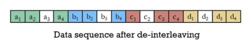
Figure 6: Interleaving example step 4: Data after de-interleaving.
This will only work if the packet lenght is a square number, therefore padding is be added in cases where this condition is not met.
This section is oudated in respect to current design. New telecommands have been designed in order to facilitate debugging, testing and providing a more thorough control of the spacecraft. These can be found on the Operations book. Reed Salomon encoding has also been dropped out. All the aforementioned changes will be reflected on future versions of the Wiki and software.
Telecommands are the mesages or instructions send by the Ground Station to the satelite that indicate it to perform a specified task. The opposite data, the one sent by the spacecraft to the GS, receives the name of telemetry.
This telecommand orders the PocketQube to do a soft reset. This is required in case of software malfunctioning when the satellite is experiencing unexpected behaviour.
The structure of this telecommand is:
Then, this content is interleaved and the output is transmitted.

This telecommand, as its own name implies, requests the exit from a state. The state desired to exit is sent as a parameter inside the telecommand.
The structure of this telecommand is:
Then, this content is interleaved and the output is transmitted.

In fact, a Two Line Element has 3 lines. The first one is for the satellite name, thus, in this case, it can be neglected. Then, two lines of 69 Bytes each contain the orbital elements from which the orbit of the satellite can be computed. This telecommand is used to update the orbit information in the PocketQube needed to propagate the orbit.
As commented previously, the maximum payload size allowed is 48 bytes (taking into account the multiples of 16). Thus, 4 packets will be needed to send the two lines of 69 bytes from the TLE because, from the 48 bytes, only 34 are reserved for data.
Two designs have been implemented given the fact that the last packet only transports 18 bytes of the TLE. The first 3 packets will follow this structure:
3 bytes of header formed by 2 bytes of PIN and 1 byte of telecommand ID,
40 bytes of the TLE orbital elements,
4 bytes of a Unix time timestamp,
1 end byte equivalent to 0xFF. Regarding the last packet, it will have the following structure:
3 bytes of header formed by 2 bytes of PIN and 1 byte of telecommand ID,
18 bytes of the TLE orbital elements,
4 bytes of a Unix time timestamp,
1 end byte equivalent to 0xFF.
22 bytes of '0''s. Each packet will also be interleaved before being sent.

This telecommand orders the PocketQube to send the payload data.
The structure of this telecommand is:

This telecommand orders the PocketQube to send the telemetry data so it does not have to wait for the beacon to be transmitted.
The structure of this telecommand is:

In the payload data transmission, since lots of packets are sent in a row, to avoid the interruption of the transmission, only a packet will be sent at the end with the information of the packets that were received and the ones that were not.
The structure of this packet depends on the number of received packets:
Then, this content is interleaved and the output is transmitted. In this packet structure, padding might be added if the number of ACK bytes is not enough to construct a packet with a length multiple of 2^#.

This packet sends the whole ADCS parameters needed to calibrate and then, when the PocketQube receives it, the calibration is carried out.
This structure will be changed in the near future.


The UPLINK CONFIG telecommand sends the desired PocketQube configuration to the satellite and once it is received, the parameters are compared to the ones stored in the PocketQube. If the parameters do not match, the values are updated.
The structure of the telecommand is:
3 bytes of header formed by 2 bytes of PIN and 1 byte of telecommand ID,
18 bytes of configuration data,
4 bytes of a Unix time timestamp,
1 end byte equivalent to 0xFF, and
11 bytes of padding to reach the next multiple of 2^#, which is 32 bytes. The configuration data can be broken into:
4 bytes of Unix time used for synchronization, - 4 bytes of communication parameters such as spreading factor, coding rate, frequency etc., - 1 byte for the KP constant (the equilibrium constant), and - 3 bytes for the battery thresholds of the nominal, the low and the critical states (one byte each).
Then, this content is interleaved and the output is transmitted.

This telecommand requests a change of receiving timeout of the PocketQube. This might be useful if the spreading factor is increased which implies slower transmissions.
The structure of this telecommand is:

This telecommand is sent when the payload must be activated either for a photo or for an RFI measurement (depending on the payload of the POCAT). All the characteristics of the photo or measurement along with the payload configuration are specified in the telecommand.
The structure of this telecommand is:
First of all, 6 bytes with information related to the photo (in case the PQ has no camera as payload these bytes are set to 0), which can be broken down into:
4 bytes of Unix time to inform when to take the next payload data acquisition,
1 byte to request a specific compression for the photo, and
1 byte to ask for a specific photo resolution. Followed by 12 bytes for the RFI measurements (in case the PQ has no monitoring receiver as payload these bytes are set to 0) divided into:
Then, this content is interleaved and the output is transmitted.

This telecommand asks the PocketQube to send its configuration packet in order to check if everything is working properly. In case something is not as expected, the UPLINK CONFIG telecommand is sent specifying the desired parameters to modify.
The structure of this telecommand is as follows:
Then, this content is interleaved and the output is transmitted.

The telemetry packet is transmitted when the ground station sends the SEND TELEMETRY telecommand. Moreover, the telemetry is also sent in the beacon packet which is transmitted every minute. Inside this packet is gathered information from different PocketQube subsystems. The global structure is:
3 bytes of header formed by 1 byte of Mission ID, 1 byte for the PocketQube ID and lastly 1 byte for the packet ID (in this case the telemetry ID), - 91bytes for the telemetry data, - 4 bytes of a Unix time timestamp, - 1 end byte equivalent to 0xFF, and - 11 bytes of padding in order to reach 48 bytes and do proper interleaving. The telemetry data can also be broken down into the different subsystem’s data:
4 bytes for the EPS. This subsystem has the following distribution of information: •1 byte to store the electrical power system voltage used
•1 byte to store the electrical power system current used
•1 byte for the battery capacity, and
•1 byte for the subsystem temperature.
3 bytes for the OBC. This subsystem information is broken into:
• 3 bits for the PocketQube state (Init, Nominal, Contingency, Sunsafe, Survival and Waiting),
• 2 bits for the Point of Load,
• 3 bits for the PocketQube state error flags,
• 2 bits for the EPS errors such as CHRG (corresponds to an error during the charging process) or FAULT (this is a generic error),
• 6 bits for the communication protocols errors such as I2C, SPI, UART errors, and
• 1 byte to store the onboard computer temperature.
14 bytes for the ADCS. This other subsystem information can also be divided into:
• 6 bytes for the information on the gyroscope,
• 2 bytes for the magnetometers information,
• 3 bytes to store the sun vector,
• 2 bits for the ADCS mode. There are two possible modes, measuring and actuating,
• 6 bits for the magnetic torquer level, and
• 1 byte for the subsystem temperature.
7 bytes for the PQ temperature: This is not a subsystem, but it is a critical topic that needs to be included in the telemetry. It is also subdivided into:
• 6 bytes for each solar panel (+X, -X, +Y, -Y, +Z, -Z), and
• 1 byte for the battery temperature.
Then, this content is interleaved and the output is transmitted.

The data packets are all sent in a row when the PocketQube receives the SEND DATA telecommand. There will be as many packets as needed in order to transmit the whole payload data.
The telecommand is formed by:
Then, this content is interleaved and the output is transmitted.

The configuration packet is transmitted from the PocketQube to the ground station when the SEND CONFIG telecommand is received. This packet has the same structure as the UPLINK CONFIG telecommand except for the 2 bytes of PIN ID which are replaced by the mission ID and the PQ ID bytes.

The purpose of this section is to conduct a complete test of the COMMS subsystem following the soldering of the board or after completing environmental tests. These tests are essential to ensure that the COMMS subsystem hardware is functioning as intended.
The entire test is outlined in the following diagram:
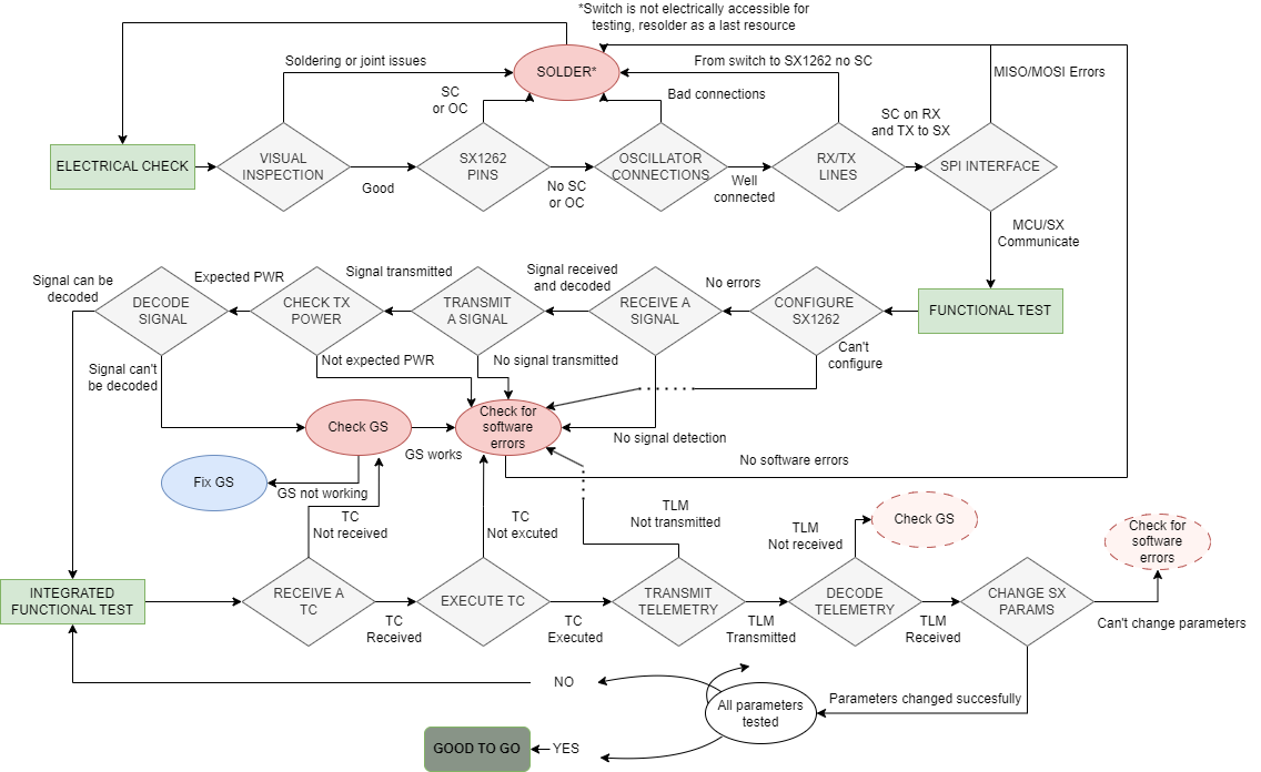
Figure 1: COMMS Development and Verification Plan.
COMMS SDV starts with a visual inspection of the soldered board, in search for easily detectable mistakes and solder issues. The next step is to manually verify the connections on the SX1262 (Transciever) pins, as OC might be common if care is not taken when soldering. The oscillator presents as a moderately hard to solder piece so it is easy and useful to ensure that the lines connecting the crystal to the SX1262 and the planes are properly set-up. A critical piece to verify is the switch, but to do so electrical checks are not easy to perform. Its status will be verified by the transmission and reception operations. RX/TX go all the way from the switch to the transciever, so a simple contituity check suffices to verify the line integrity, Finnally, with the help of the OBC the SPI interface is tested to verify communications.
As communication between the MCU and the SX is ensured it is time to test the basic operations to be performed by the COMMS subsystem, mainly receival and decoding as well as transmission of signals at appropiate power. Several points of failure appear in these steps, mainly software errors and GS errors. It might also occur that the previous electrical check did not completely sort out all isues, creating the need for further hardware inspection.
The final steps are to verify the board and susbsystem is to test several operations to be done by it. Telecommands are to be received, executed and telemetry is to be transmitted and decoded by the GS. Finally it is optimal to test the system with different configurations as parameters might be changed on-the-fly during the mission. If this step is accomplished the board is considered good to go.
The purpose of this section is to conduct an electrical check of the COMMS subsystem following the soldering of the board or after completing environmental tests.
Always ensure you're grounded to prevent static electricity from damaging the electronic components on the board.
| Requirement ID | Description |
|---|---|
| COMMS-EC-001 | All components and connections shall be visually inspected to ensure proper soldering, absence of damage, and correct placement of wires. |
| COMMS-EC-002 | Each SX1262 pin shall be securely connected to its corresponding circuit point, with no shorts or floating pins present. |
| COMMS-EC-003 | The oscillator shall be checked to ensure its connections are properly soldered and it is operating at the specified frequency. |
| COMMS-EC-004 | The receive (RX) and transmit (TX) lines shall be inspected to confirm they are properly wired, with no interference or signal degradation. |
| COMMS-EC-005 | The SPI interface shall be validated to ensure correct wiring and successful communication between the microcontroller and the SX1262. |
| COMMS-EC-006 | All solder joints shall be inspected to verify they are strong and free from defects, with any weak joints re-soldered as needed. |
| Description | Pass Criteria | Fail Criteria |
|---|---|---|
| Visual inspection of components, soldering, and wire placement. | Components and lines are securely soldered and correctly positioned, with no visible cracks in the soldering or components, melted parts, or misaligned elements. | Improper soldering, damage, or incorrect placement. |
| Secure connections for SX1262 pins, with no shorts or floating pins. | All pins are securely connected, no shorts or floating pins. | Pins are loose, shorted, or floating. |
| Check oscillator connections and frequency. | Oscillator is correctly soldered and operates at the right frequency. | Faulty connections or incorrect frequency. |
| Inspect RX and TX lines for proper line and signal quality. | RX and TX lines are correctly connected with no signal issues. | No signal, interference, or signal degradation are observed. |
| Validate SPI interfaces and communication. | SPI is correctly connected and communication is successful. | Incorrect connection or communication failure. |
| Inspect solder joints for strength and defects. | Solder joints are strong and defect-free. | Weak or defective joints require re-soldering. |
| Step - ID | Description |
| EC-TEST-01 | Using a microscope or equivalent tool, perform a visual inspection of the OBC-COMMS board to check for damaged components or traces, as well as displaced or missing components, and cracks in the solder joints. If any damaged elements are identified, replace them or conduct additional tests to assess their functionality. |
| EC-TEST-02 | Using a multimeter, verify that all pins of the transceiver (SX1262) are properly soldered, correctly positioned, and free of any unwanted short circuits or open circuits. |
| EC-TEST-03 | Repeat the previous step for the oscillator connections. |
| EC-TEST-04 | Use a multimeter to verify that the entire RX-TX chain is free of any unwanted shorts or open circuits. Pay extra attention to the switch, as it has 6 pins in a confined space. |
| EC-TEST-05 | After inspecting the COMMS subsystem, the final step is to verify the connections between the transceiver and the On-Board Computer. Specifically, use a multimeter to ensure that all SPI connections are secure. The pins to check include SX1262_NSS, SCK, MOSI, MISO, SX1262_NRST, and SX1262_BUSY. |
If the electrical check is successful, proceed to the functional testing of the COMMS subsystem. Keep in mind that in some cases, such as after a vibration test, the board may sustain subtle damage, so proceed with extra caution!
The purpose of the functional test is to achieve a successful transmission using the OBC-COMMS board.
| Requirement ID | Description |
|---|---|
| COMMS-FT-001 | The SX1262 configuration parameters (SF=11, CR=4/5), including frequency (868 MHz), modulation (LoRa), and power settings, shall be correctly set for the test. |
| COMMS-FT-002 | The device shall transmit a signal that is detectable at the intended range (frequency and power) with minimal signal degradation. |
| COMMS-FT-003 | The transmission power level shall be verified to meet specified limits and be consistent with expected output. |
| COMMS-FT-004 | The device shall successfully receive signals without interference or loss of quality during the test. |
| COMMS-FT-005 | The device shall decode incoming signals accurately without errors during the functional test. |
| Description | Pass Criteria | Fail Criteria |
|---|---|---|
| The SX1262 configuration parameters (SF=11, CR=4/5), including frequency (868 MHz), modulation (LoRa), and power settings, shall be correctly set for the test. | Parameters are set correctly as per specification (SF=11, CR=4/5, frequency=868 MHz, modulation=LoRa, power at specified level). | Parameters are incorrectly set, or any configuration setting is missing or erroneous. |
| The device shall transmit a signal that is detectable at the intended range (frequency and power) with minimal signal degradation. | Signal is transmitted and detected within the specified range, with acceptable signal quality and minimal degradation. | Signal is not detectable, outside the intended range, or shows significant degradation. |
| The transmission power level shall be verified to meet specified limits and be consistent with expected output. | Transmission power meets specified limits and aligns with expected power output. | Transmission power is inconsistent with expected output. |
| The device shall successfully receive signals without interference or loss of quality during the test. | Signals are received with clarity, no interference, and within acceptable quality limits. | Signal reception is poor, shows interference, or lacks quality. |
| The device shall decode incoming signals accurately without errors during the functional test. | Signals are decoded correctly without errors, and data integrity is maintained. | Decoding fails, produces errors, or results in data integrity loss. |
| Step - ID | Description |
| FT-TEST-01 | Connect the OBC-COMMS board to a computer using the ST-LINK v2, concretely connect the RST, 3.3V, GND, SWCLK and SWDIO pins to the board. |
| FT-TEST-02 | After connecting the board to the laptop using an ST-LINK, upload the code to the board. You may want to add breakpoints to examine each step of the transmission process in detail. |
| FT-TEST-03 | After flashing the code, use a Spectrum Analyzer to visualize the transmission’s power, frequency, and other parameters more effectively. |
| FT-TEST-04 | After verifying the basic parameters of the transmitted signal, proceed to test the Ground Station's ability to correctly decode the signal. Configure the a TinyGS for a reception test of the transmitted signal. |
| FT-TEST-05 | Transmit a signal, ideally containing user-generated telemetry data, and verify that the Ground Station has accurately received and decoded all transmitted information. This test can be repeated with different types of data, such as payload data. |
| Requirement ID | Description |
|---|---|
| COMMS-IFT-001 | The system can receive telecommands, including those consisting of multiple packets. |
| COMMS-IFT-002 | The COMMS system successfully executes telecommands upon correct reception and generates a response if the telecommand requires it. |
| COMMS-IFT-003 | Once a response is generated, the COMMS subsystem transmits it accurately at the specified frequency (868 MHz), output power (22 dBm), spreading factor (11), and coding rate (4/5). Same requirement applies for the telemetry which is sent periodically by the spacecraft. |
| COMMS-IFT-004 | The received telemetry and/or telecommand is correctly decoded by the Ground Station. |
| COMMS-IFT-005 | All parameters updated via telecommand on the PocketQube are accurately applied, including configuration adjustments and payload activation settings. |
| Description | Pass Criteria | Fail Criteria |
|---|---|---|
| x | x | x |
| x | x | x |
| x | x | x |
| x | x | x |
| Step - ID | Description |
| x | x |
| x | x |
| x | x |
| x | x |
| x | x |
The aim of this document is to clearly explain the tests performed during the delevolpment of the subsystem.
This document is based on current but also previous versions both of hardware and software and as such be followed with care.
Antenna impedance matching is a crucial aspect in the design and operation of radio frequency systems. Impedance matching involves adjusting the impedance of the antenna to match the impedance of the transmission line or the RF source to which it is connected. The objective of the test will be to determine the length of the quarter wavelength monopole antenna for the satellite.
| Requirement ID | Description |
|---|---|
| AMT - 01 | The antenna should exhibit impedance values closely matching the specified target impedance across the defined frequency range (868 MHz). |
| AMT - 02 | Return loss values should be high, indicating a low amount of power reflected back towards the source and efficient power transfer. |
| AMT - 03 | The antenna should demonstrate acceptable impedance matching and performance across the specified bandwidth(125kHz). |
| Parameter | Pass Criteria | Fail Criteria |
|---|---|---|
| Return Loss | Return Loss < -10 dB (lower values are better) | Return Loss > -10 dB (indicating poor matching) |
| Standing Wave Ratio (SWR) | SWR < 2:1 (lower values are better) | SWR > 2:1 (indicating poor impedance matching) |
| Impedance Matching | Impedance matched to system requirements | Significant deviation from desired impedance |
| Radiation Pattern (optional) | Symmetrical and aligned with specifications | Irregular pattern, beam tilting, or distortions |
| Step - ID | Description |
| AMT\_S-01 | Prepare the Testing Environment:
|
| AMT\_S-02 | Calibrate the Vector Network Analyzer:
|
| AMT\_S-03 | Connect the Antenna:
|
| AMT\_S-04 | Measure the Antenna Impedance:
|
| AMT\_S-05 | Analyze Measurement Results:
|
| AMT\_S-06 | Optimize and Fine-Tune (if needed):
|
| AMT\_S-07 | Save and Store Data:
|
The test was conducted in the autumn of 2022, and the outcomes are as follows:

As can be seen in the figure above, the final antenna had RL(dB) = -10 for the operating frequency. Moreover, the bandwidth of the antenna is approximately 15 MHz.
The result obtained from this test, however, is quite surprising: the antenna length must be 3.5 cm, which is much lower than what was theoretically calculated (8.64 cm). The reason behind this result could be the non-ideal ground plane of the monopole.
Obtained antenna lenght is 3.5 cm, lower than what was theoretically calculated (8.64 cm).
Test should be redone with the final version of the PocketQube.
The objective of this test is to validate the correct operations of the COMMS layout in the PocketQube with the OBC&COMMS board.
| Requirement ID | Description |
|---|---|
| OCBT - 01 | Be able to see MISO, MOSI, SCK, SX1262-NSS, SX1262-NRST and SX1262-BUSY signals. |
| OCBT - 02 | Be able to decodify MISO, MOSI and SCK |
| OCBT - 03 | MISO, MOSI and SCK decodification must match expected results of the datasheet. |
OBC&COMMS with only used pinouts:

If we zoom into the COMMS chip we get the following:
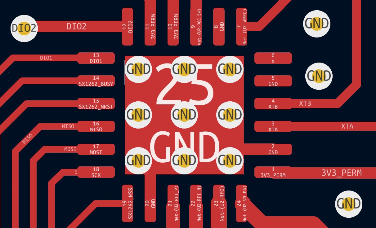
We'll measure the following pins: MISO, MOSI, SCK, SX1262_NSS. These are the only ones available for comparison with the expected values outlined in the datasheet.


We will connect the ST-LINK v2 to a PC for flashing code. The SWDIO, SWCLK, and 3.3V ports of the ST-LINK v2 will link to pull-up resistors shown in the following image before connecting them to their respective pins. Meanwhile, the other ports (GND and RESET) will be directly linked to the board.

To verify the functionality of the COMMS chip, we'll compare the obtained results with the expected specifications outlined in the SX1262IMLTRT datasheet.
The test will be deemed successful if our obtained results align with those specified in the datasheet. If they don't correspond, the test will be considered unsuccessful.
| Step ID | Description | Pass/Fail Criteria | Actual | Passed(Y or N) |
| CS - 01 | Prepare the setup explained in the previous step | Flashing must be successful, a "successful message" must appear | We encountered a lot of issues when flashing due to poor connections, after many attemps we successfully flashed | Sometimes, had to repeat multiple times until it worked |
| CS - 02 | Flash code, we used the main program (Project>>Build All + Run>>Debug As>>1STM32C...) | |||
| CS - 03 | Using Saleae, check all pins of the SX1262 chip, especially MISO, MOSI, SCK and SX1262-NSS | Just after flashing we must see signals in all these pins | Only MISO had a visible signal, the others had not | No, no signal was spotted in MOSI, SCK and SX1262-NSS. |
| CS - 04 | Once we have simultaniously captured MISO, MOSI and SCK, decodify the signal | Comparing with the SX1262 datasheet, the decodification must be the one we expected | Since we only obtained the MISO signal, it has been impossible for us to decode | No |
We encountered several issues while working on the project. Firstly, we faced weak connections between the board and the computer for CS-01 and CS-02, which resulted in several days of troubleshooting. We had to solder connectors to establish a stable connection, but the board remained fragile, and we couldn’t touch it much.
Moving on to CS-03, we encountered three major issues. The first issue was with the tool we used for decodification. We needed three ports to capture all three signals (MISO, MOSI, and SCK) simultaneously, so we had to switch from PicoScope to a Saleae device. The second issue was the small size of the chip and connections, which made it extremely difficult (if not impossible) to capture all signals simultaneously. We recommend adding testing pins to the board in future versions. Finally, the third issue was with the decodification process itself. We could only observe MISO, SX1262_NRST, SX1262_NSS, XTA, and XTB signals. Since we also needed MOSI and SCK signals to decode the signal, we were unable to do so. We also checked the power pins going to the SX1262 and found no issues.
As for CS-04, we were unable to compare it with the datasheet since we couldn’t decode it.
During the project, we faced several issues. As previously mentioned, we encountered anomalies during the test, including fragile connections, small pins on the chip that made it difficult to check all signals simultaneously, and no signal for MOSI and SCK. Unfortunately, we were unable to decode the signal.
As the COMMS subsystem relies heavily on this crucial test, essential for communication testing, we've opted to temporarily skip it. Instead, we will use a spectrum analyzer to verify if the chip is transmitting signals. If successful, it confirms effective communication between the OBC and COMMS chips. However, if no signals are detected, the issue may lie in the connections/design of the board.
Due to the outcomes of the OBC-COMMS board test, an alternative method is required to validate ongoing communication between the OBC and COMMS chips. To achieve this, we plan to establish communication between a TinyGS and the OBC-COMMS board, effectively simulating the connection between a ground station and our satellite. Furthermore, attenuations will be introduced later in the process to mimic the conditions present in space.
| Requirement ID | Description |
|---|---|
| RXTX - 01 | Be able to transmit using a TinyGS. |
| RXTX - 02 | Be able to receive the transmitted data using the SX1262. |
| RXTX - 03 | Possess the capability to respond to specific telecommands by transmitting a reply. |
| RXTX - 04 | Have the capability to initiate communication between the TinyGS and the OBC-COMMS while incorporating attenuations. |
| RXTX - 05 | Possess the capability to process telecommands and provide responses while incorporating attenuations. |


For the initial and fundamental phase of our test, the setup is as follows:
One computer will be connected to a TinyGS, while the other computer will have a Nucleo+LoRa module connected to it. This configuration allows us to verify the transmission capability of the TinyGS and the responsiveness of the board (initially represented by an STM32 Nucleo + LoRa module).
The setup for the STM32 Nucleo + LoRa module is the following:

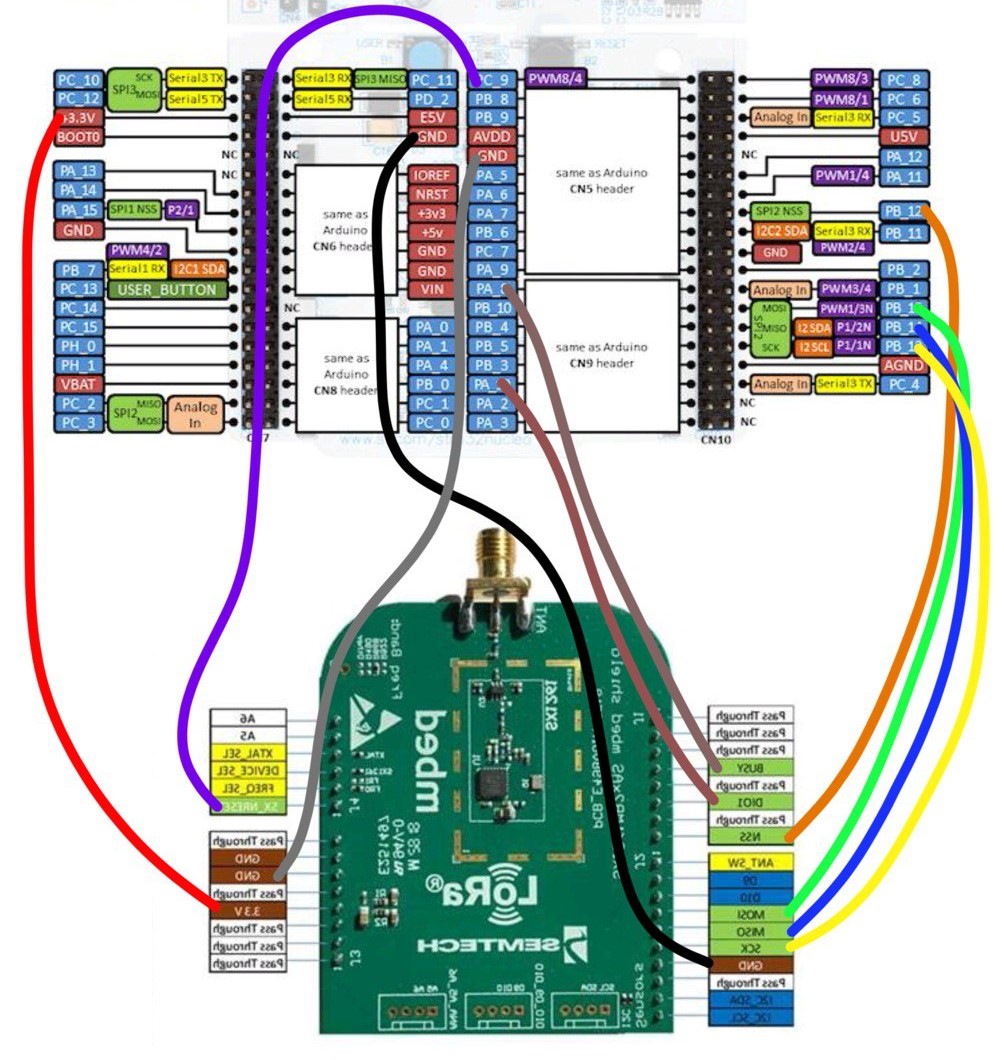
After successfully testing this setup, the next configuration is as follows:
Instead of the Nucleo+LoRa, we will integrate the OBC-COMMS board from the OBC-COMMS board test.
As we advance in the testing process, we will introduce a variable attenuator in either reception or transmission.
Throughout the experiment, a spectrum analyzer will be employed to detect the signals transmitted, while the TinyGS console will be utilized to monitor both sent and received data.
The experiment will be deemed successful if the specified requirements are fulfilled, signifying our ability to transmit effectively using the TinyGS, and the OBC-COMMS board responds as anticipated, both in the presence and absence of attenuation.
The initial phase of this test involves configuring and preparing a TinyGS station. Since a similar station has been utilized in previous tests, please refer to the instructions provided in the "ᴾᵒCat Testing >> ᴾᵒCat SSVs >> COMMS Software SSV" section for guidance.
Once our TinyGS is configured we can test its transmission capabilities by sending one of the telecommands shown in the TinyGS console. For checking the correct transmission we will used a spectrum analyser. 
If encountering transmission difficulties, we can attempt communication between two TinyGS units. This approach allows us to showcase the capability of our TinyGS in both sending and receiving data. The necessary steps involve configuring a second TinyGS (just like we did with the first one) and issuing a telecommand, with the option to utilize the "p" command for sending a test packet.
Upon confirming the proper functionality of the TinyGS, the next step is to connect the STM32 Nucleo + LoRa module to the computer. Subsequently, we will flash our code into it to activate the reception mode of the SX1262 (LoRa module). Finally, we will initiate transmission using the TinyGS and observe if the STM32+LoRa module responds. For this test we will only take into account the "FLASH" and "COMMS" tasks.
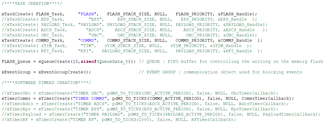
After confirming the correct functionality of the code on the STM32 Nucleo + LoRa module, we can proceed to the next stage of utilizing the board. If the preceding tests yield success, but this phase encounters issues, we can confidently conclude that the issue lies in the hardware rather than the software, thereby narrowing down the potential sources of errors.
If all the preceding steps are successful, the next phase involves experimenting with attenuators to simulate the conditions our system will encounter in space. Common attenuators and a variable attenuator will be employed for this purpose. The objective of this step is to assess the feasibility of transmission under various influencing factors such as distance, speed, angle of the antennas, and other relevant parameters.
The configuration of the TinyGS for transmission and reception at 868MHz was completed successfully.
The TinyGS exhibits the ability to both transmit and receive data, as exemplified by the successful demonstration using two TinyGS units. In the event of possessing only one TinyGS, we can showcase the effective operation of the ground station by employing a spectrum analyzer and receiving signals from satellites that are using the TinyGS network.
Upon flashing our code into the Nucleo and transmitting diverse telecommands with TinyGS, we discovered that the LoRa module failed to transmit responses to the telecommands as expected. Following a thorough and extensive investigation, we identified the root cause of the issue: during reception, the reception buffer requires slightly more time before decoding to effectively process the incoming packets. To address this issue, we implemented a solution by incorporating a small delay. Following this adjustment, we have successfully achieved the reception and response to telecommands sent by TinyGS, as demonstrated in here:
We will commence with telecommands that do not necessitate a response from the PocketQube. To verify proper functionality, we will insert breakpoints within each of these states for testing.


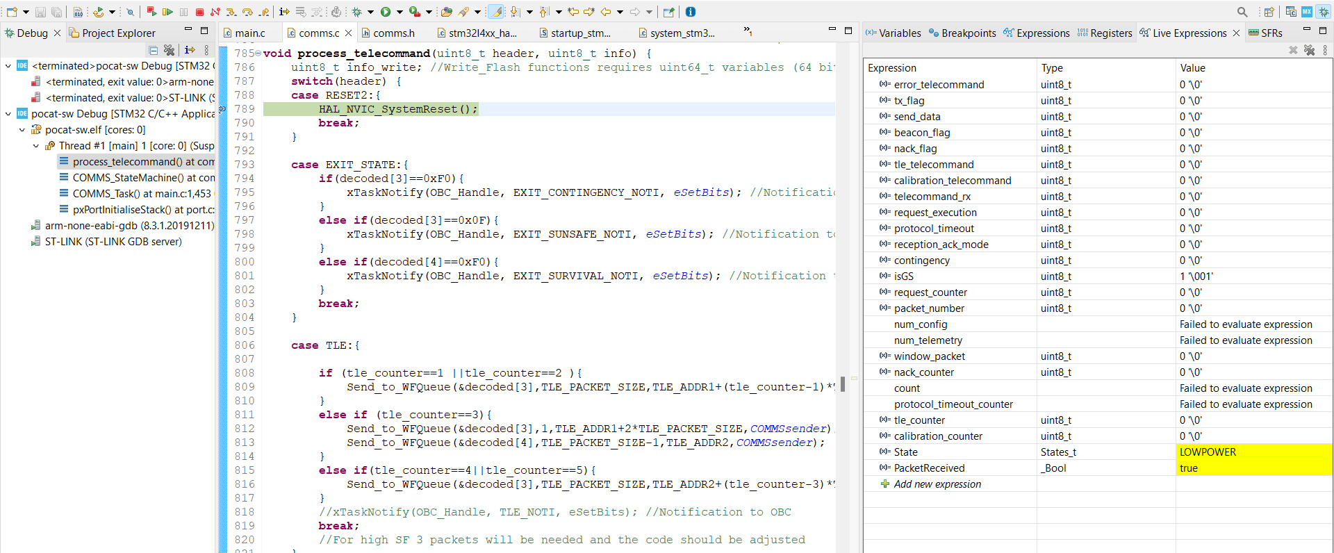
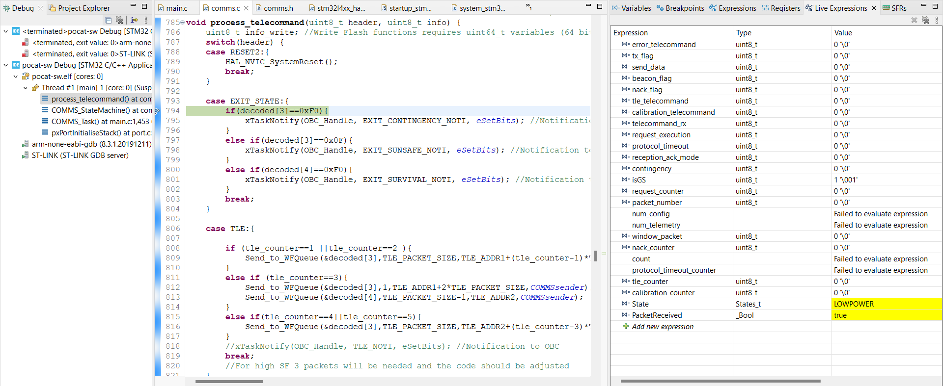


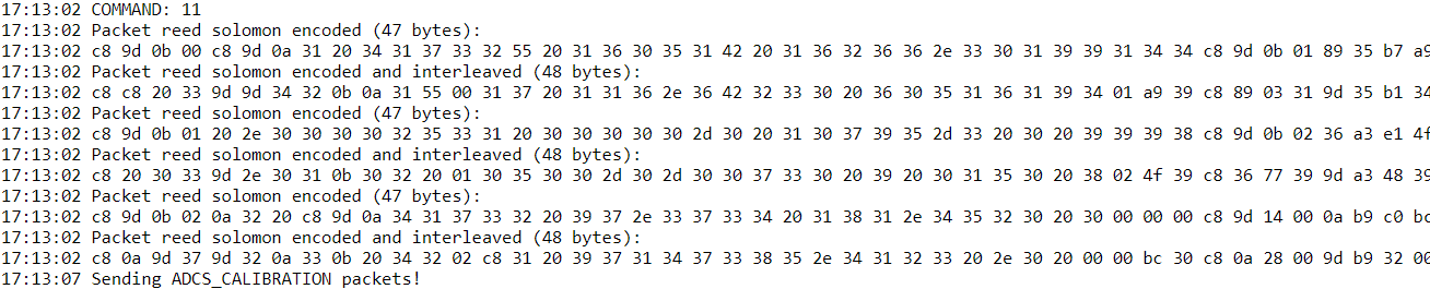
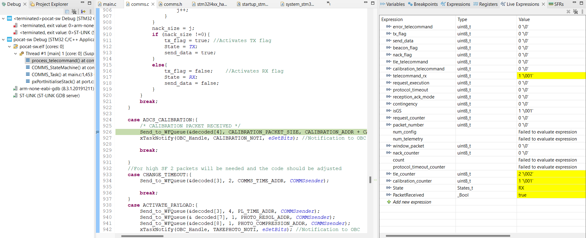
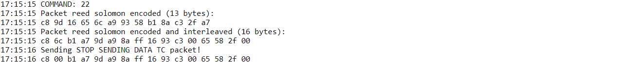


Subsequently, we will perform tests on all telecommands that necessitate a response from the satellite. To test these telecommands, we can choose to either insert breakpoints or examine the responses from the TinyGS terminal.


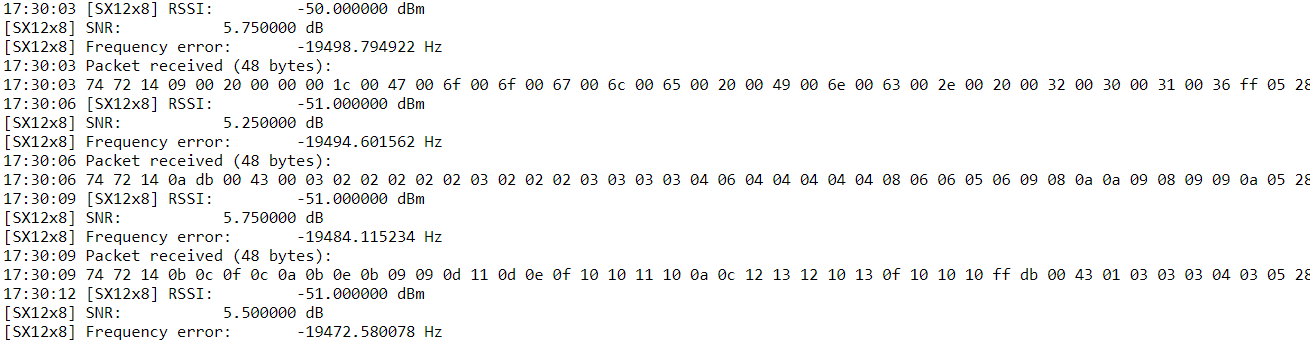

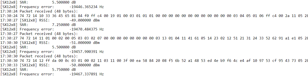


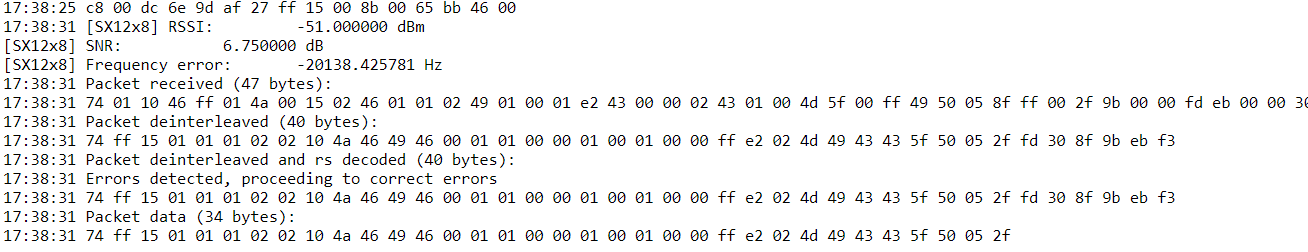

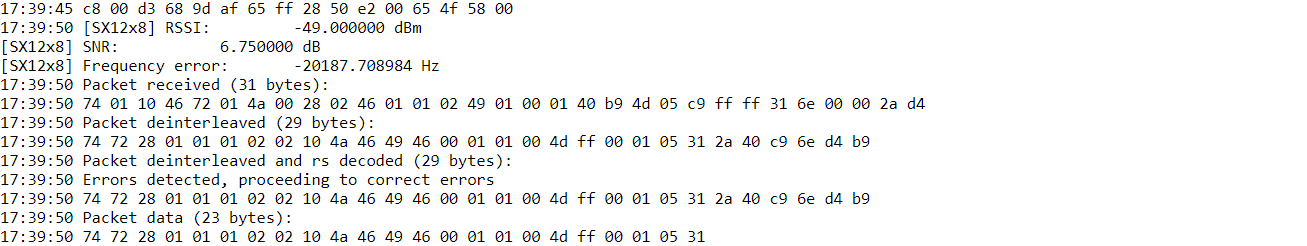
We can affirm that all telecommands have been successfully transmitted by TinyGS, processed by the Nucleo+LoRa, and appropriately answered when required.
Following the success of the previous step, we proceeded to integrate the actual OBC-COMMS board. However, the experiment deviated from the plan due to several issues:
While we initially anticipated hardware-related problems, a careful examination of variable values (such as the COMMS state or PacketReceived) suggests a potential issue with the OBC and task management rather than the hardware.
To address these issues, several actions were taken:
UPDATE: Errors were detected on the OBC-COMMS board
1) Mirroring error in one of the OBC crystal oscillator:
The error has already been corrected in the newest OBC-COMMS PCB design. The clock was removed from the board for this test as

2) Issue with the transceiver clock capacitors. Both transceiver crystal oscillators were removed as per the transceiver datasheet: "The SX1261/2 does not require the user to set external foot capacitors on the XTAL supplying the 32 MHz clock. Indeed, the device is fitted with internal programmable capacitors connected independently to the pins XTA and XTB of the device. Each capacitor can be set independently, balanced or unbalanced to each other, by 0.47 pF typical steps."
Both capacitors were removed.
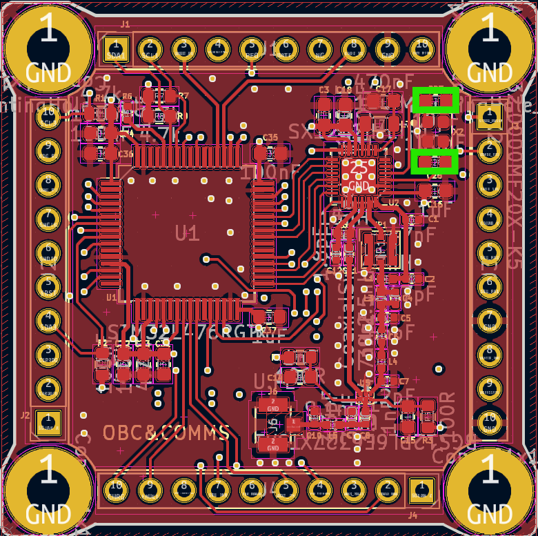
After implementing the commented modifications to the board, the testing was resumed:
TBD.
As we've been reviewing the test results, several issues were encountered during the process:
During step 3, an issue arose during the reception process, which was successfully resolved by introducing a slight delay. The issue caused the system to "ignore" the sent telecommands.
In step 4, the COMMS subsystem persisted in LOWPOWER mode, necessitating the removal of tasks to facilitate the test. This indicates an ongoing challenge with the OBC subsystem task.
Another issue in step 4 involved the reception of numerous packets from unidentified sources. To address this, further solutions are needed, and the possibility of conducting tests within an anechoic chamber is being considered for better-controlled testing conditions
The issue pertaining to OBC task management must be tackled, as it seems to be the primary cause of the anomalies we discussed.
Furthermore, we must also tackle the problem of receiving numerous packets, as it hinders the reception of the genuinely important ones.
At the very least, we can affirm that the COMMS code is functioning correctly, and the OBC-COMMS board, equipped with the quarter-wavelength antenna, is capable of successfully receiving packets.
This test aims to evaluate the chosen Dyneema for the antenna deployment. It involves measuring the time taken for the material to melt under atmospheric conditions.


If Dyneema melts within the range of 10 to 15 seconds at 3.3V and 450mA, the test can be deemed successful. However, if it takes longer or fails to melt, the test will be considered unsuccessful.
The knot is connected to the resistor and the power source is connected. We used the weight of the lateral board with the antenna to simulate some pressure.
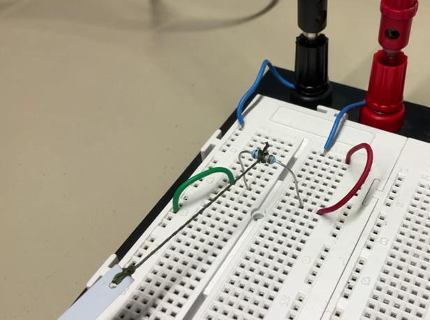
The knot starts showing signs of degradation as the temperature of the resistor increases.

The knot melts and the pressure provoques the antenna to deploy.

Some calculations:
Power (W) = Voltage (V) * Current (A) = 3.3 * 0.45 = 1.485 W
Energy consumed (J) = Power (W) * Time (s) = 1.485 * 14 = 20.79 J
None. After repeating this test, it was determined that it needed to be redone as the dyneema did not burn, but melted instead.


Possible problems with the EPS. Redo the test.
This experiment will undergo repetition within a vacuum chamber due to the differing thermal properties in such conditions. Dyneema is expected to exhibit a significantly faster melting rate as heat transfer with the absence of air in space is not a factor.
The primary goal of this test is to validate the satellite's antenna deployment. This step is mission-critical as its proper function is pivotal for the transmission and reception of data by the satellite.
This test might (if possible) also test the comunications with the deployed antenna.
| Requirement ID | Description |
|---|---|
| ADTR - 01 | Dyneema must melt in less than 15 seconds in vacUum conditions. |
| ADTR - 02 | The antenna must deploy correctly, meaning that it should remain nearly completely straight after deployment. |
| ADTR - 03 | The spacecraft must be able to communicate with the ground station after antenna deployment |
If the Dyneema melts in under 15 seconds in vacuum conditions and the antenna remains straight post-deployment, we will deem the antenna deployment test successful.
Prior to conducting a test in the vacuum chamber, it is imperative to meticulously examine the feasibility of the test in atmospheric conditions. While the results may vary, the ultimate conclusion remains the same: if the dyneema melts in atmospheric conditions, it will likewise experience the same outcome in vacuum conditions.
To carry out this preliminary test, a PocketQube with, at a minimum, the OBC-COMMS and EPS subsystems is required. The EPS can be powered either by a direct power source or a battery. The activation of the thermal knife will be done using cables activating the BURNCOMMS pins from the OBC-COMMS board.
The initial phase involves preparing the entire test setup, a critical step that will determine the feasibility of conducting the test under vacuum conditions. For this we will follow the Thermal Vacuum Chamber Operations Manual.
In our specific scenario, the test chamber will accommodate a PocketQube containing, at a minimum, the OBC-COMMS and EPS subsystems. The EPS will include a battery, serving as the power source for the thermal knife.
To activate the thermal knife, control over the OBC-COMMS board will be facilitated through cables.
After placing the PocketQube in vacuum conditions, we can initiate the antenna deployment test. To do this, we will activate the BURNCOMMS pin on the OBC-COMMS board. This pin is connected to a low-impedance resistor, which, in turn, is linked to the dyneema for the antenna deployment.
What we will do once we activate the pin is mesure the time it takes for the dyneema to test. We can later calculate the power consumed and perform adjustments if necessary.
This step is considered optional due to uncertainties regarding its feasibility in our small vacuum chamber. The objective is as follows: utilizing an additional antenna within the vacuum chamber, potentially a TinyGS, we aim to test the deployed antenna by establishing direct communication between the PocketQube and the auxiliary antenna, simulating a Ground Station. Attenuators may be employed to replicate challenging space conditions. The primary goal is to transmit telecommands and assess whether the satellite can respond as anticipated.
# Software Tests as RunThe aim of this document is to clearly explain the tests performed during the delevolpment of the subsystem.
This document is based on current but also previous versions both of hardware and software and as such be followed with care.
The module used is the LILYGO ® TTGO-ESP32 LoRa32 V2 868/915MHZ which has been selected among the ones supported by the TinyGS software.

### PocketQube module
The MCU used for the OBC-COMMS is STM32L476RG. This MCU family is chosen because STM32 are characterised by being ultra-low power microcontrollers and power saving is crucial for the satellite.

The PoquetQube transceiver module used is the Semtech SX1262.

This module has the following characteristics:
In order to test the software in the ground station, this is the setup needed to follow:
1. Heltec WiFi LoRa 32 V1 (433MHz 863-
2. 928MHz versions).
3. Heltec WiFi LoRa 32 V2 (433MHz 863-928MHz versions).
4. TTGO LoRa32 V1 (433MHz 868-915MHz versions).
5. TTGO LoRa32 V2 (433MHz 868-915MHz versions).
6. TTGO LoRa32 V2 (Manually swapped SX1267 to SX1278).
7. T-BEAM + OLED (433MHz 868-915MHz versions).
8. T-BEAM V1.0 + OLED.
9. FOSSA 1W Ground Station (433MHz 868-915MHz versions).
10. ESP32 dev board + SX126X with crystal (Custom build, OLED optional).
11. ESP32 dev board + SX126X with TCXO (Custom build, OLED optional). (k) ESP32 dev board + SX127X (Custom build, OLED optional).
12. The one used in this project is the TTGO LoRa32 V2 868-915MHz.
Join the TinyGS Telegram channel at the following link https://t.me/joinchat/
DmYSElZahiJGwHX6jCzB3Q.
Once in the Telegram general TinyGS channel, open a private chat with their bot
@TinyGS personal bot to ask for the MQTT credentials as in the following figure.
Figure 8.2: MQTT credentials.

Download the TinyGS uploader from this link https://github.com/G4lile0/ TinyGS/releases, select the port, and then flash the firmware.

The first time the board is flashed, it creates an AP called ”My TinyGS”. Connect to that network, open a web browser, navigate to 192.168.4.1 and the TinyGS menu will appear.
Click on the button ”Configure parameters” and enter the following parameters specific to the ground station:
Clone this repository https://github.com/juliatribo/TinyGS and flash in the board using PlatformIO.
Connect the PC to the same WiFi configured in the TinyGS and wait for the ground station to start. Once the TinyGS has been configured it will show an IP on the display. Open a web browser and navigate to the given IP.
Finally, on the website click on the station dashboard. Introduce the user: admin and the password configured before. Then, the terminal of the ground station will show up and the test can begin.
**To connect an already existing UPC NanoSat Lab TinyGS, follow these steps:**
The STM32L476RG MCU setup is the following:

Once all the set-up is ready, click on the Station Dashboard from the tinyGS and the terminal will appear. 
In this terminal, in the enter command line, the ID (in decimal) corresponding to the telecommand which needs to be tested must be entered. In the above list, all the options are displayed. When the enter button is pressed, the corresponding message is sent to the PocketQube. A detailed explanation of the content of the packets is in the COMMS Software page. 
On the one hand, to test the telecommands which don't have a response from the PocketQube, a breakpoint must be placed in the PocketQube code to check if the encoding and decoding have been successful: 
On the other hand, to test telecommands with a response from the PQ, in particular, Send Telemetry and Send Config no breakpoint is needed, because the response is shown in the TinyGS terminal: In this picture, the blue rectangle is the PQ response. The green bytes correspond to a byte corrected thanks to Reed Solomon (it was a forced error).
Then this packet is sent to the MQTT broker as well and then it can also be seen in the TinyGS web app  Note that this packet is classified as a Norby packet and it is supposedly located below New Zealand which are false statements. This is because the Kaity structure of the NanoSatLab PocketQube has still not been sent to the TinyGS team, so the TinyGS decoder does not know how to interpret the information provided in the packet.
In case of not being able to properly receive the telemetry or configuration, a NACK packet is sent to inform the satellite that a retransmission is needed. To test it, a CRC error has been forced. 
And finally, to test the Send Data, a lot of packets are sent in a row (without encoding): 


After all the packets are received, an ACK packet is sent to the PQ indicating which packets were properly received. It can be noted that the second packet is not properly received since there is a CRC error. In the ACK packet, after the header (which has 3 bytes), comes a vector with a length equivalent to the number of packets sent. If a packet is not received correctly, the byte with the index equal to the number of the packet failed is 0x0, otherwise, is 0x01. This is why the second byte of this vector is 0x0, because the second packet failed in this case.
Once the PocketQube receives the ACK, it sends back the requested packets. As can be noted, at the bottom of the last figure, the satellite has retransmitted the ordered DATA packet. It is known that this retransmitted packet is the corrupted one because its third byte (the data packet counter) is equal to 0x01, hence taking into consideration that the data packet counter starts at 0x00, this is the second packet.
None.
We are capable of establishing a communication between a Ground Station and a STM32 Nucleo + LoRa module (simulating the PocketQube).
The goal of this test is to validate the proper functioning of the ADCS calibration function, ensuring that the magnetometer is accurately calibrated as anticipated.
| Requirement ID | Description |
|---|---|
| ADCSCAL - 01 | The ADCS calibration telecommand is correctly received and processed. |
| ADCSCAL - 02 | The instruments of the ADCS subsystems are correctly calibrated. |
The test setup for this experiment is straightforward:
Establish a connection between the OBC-COMMS and ADCS boards, enabling seamless information transfer from COMMS to the ADCS subsystem.
Prepare a ground station, with the option to use attenuators to replicate space conditions, we will be sending the telecommand from here.
Following successful calibration, employ a rotating machine to simulate the satellite's rotation in all directions. All data will be read using a computer.
The sole instrument undergoing calibration is the magnetometer. To assess its accuracy, we can perform rotations in all directions and examine whether the obtained results form a perfect sphere. Successful calibration is indicated if the data conforms to a spherical shape; conversely, a lack of conformity signifies an unsuccessful calibration.
Step one involves establishing communication between the ground station and our PocketQube. To achieve this, we will follow the steps outlined in several previous tests, as explained in the preceding test or the RX-TX test.
Upon establishing communication, the next step is to send the ADCS calibration telecommand. To verify the correct reception and execution of the ADCS calibration, breakpoints can be strategically placed within the process telecommand function for monitoring.
Upon receiving the telecommand and uploading the calibration, the success of the calibration can be demonstrated by measuring the magnetometer in all three axes. The results can then be plotted using a computer, and a successful calibration is indicated by the formation of a perfect sphere in the plotted data. For rotating at a constant rate we can use a rotating wheel.
The objective of this test is to prove that the recent modifications of the code have solved the issue we had regarding the reception and registering of longer than 3 packet telecommands.
| Requirement ID | Description |
|---|---|
| MULPT - 01 | Be able to transmit all packets using a TinyGS. |
| MULPT - 02 | Be able to receive and register all the packets. |
Prepare the ground station and Nucleo + LoRa, as explained in previous tests (TinyGS test for example). If we choose to use the OBC-COMMS board instead, the setup should be the following:

If the stipulated conditions are fulfilled, specifically, successful transmission, reception, and registration of telecommands with multiple packets, we will deem this test as successful. The telecommands that satisfy these criteria include the transmission of TLE telecommands and the execution of ADCS calibration telecommands.
Once the Ground Station and the receiving component of our system (either STM32 Nucleo + LoRa or the OBC-COMMS board) have been set up, the remaining task is to transmit either the TLE telecommands or initiate the execution of ADCS calibration telecommands.

Once the telecommand is sent the COMMS subsystem should be receiving the telecommand (if not, check RX-TX test in COMMS SSV testing).
Once the telecommands are received we can check that they have been registered as planned using the Utility program (the one we use to check registers).
Both telecommands can be sent by the ground station.
Still cannot solve the issue where only a part of the packets are reveived. No appearing problem with the reception buffer.
Possible solution is to separate the TLE telecommand in 2 separate telecommands, a first part with 3 packets and a second part with 2 packets. Test will need to be redone.
Currently, the telecommand contents are hardcoded, which is not ideal. The goal is to enable the modification of telecommand contents without the need for code recompilation. Changes were made to the code to address this issue, and this test plan aims to demonstrate the effectiveness of these modifications.
| Requirement ID | Description |
|---|---|
| NHTT - 01 | Transmission of the telecommands is done correctly. |
| NHTT - 02 | Reception and processing of the telecommands is done correctly. |
| NHTT - 03 | Registers are uploaded. |
Set up both the ground station and reception modules according to the instructions provided in the previous tests.
The success criteria for this test involve the accurate transmission, reception, and correct processing of telecommands. The test will be deemed successful if these tasks are executed correctly.
After preparing the ground station and the COMMS subsystem we can begin transmiting the telecommands.
After receiving and processing the telecommands, the next step is to verify the accurate storage of information by the On-Board Computer. It is essential to ensure that the information is stored efficiently and that the addresses of the stored values are no longer hardcoded. To perform this verification, tools such as "Utility" can be employed to inspect the registers and confirm the correct storage of information.
The objective of this test is to take a picture with the VGA Camera (P/L1), ask for it through a telecommand (SEND_DATA), and receive it successfully. The test will be done without the use of TinyGS as it was suspected it was a source of errors (MQTT).
| Requirement ID | Description |
|---|---|
| VCT - 01 | Take a picture with the VGA Camera connected to OBC-COMMS. |
| VCT - 02 | Receive a TTL (SEND_DATA) and execute it. |
| VCT - 03 | Be able to receive the data sent. |
Prepare the OBC-COMMS PCB + Lateral Board, as explained in previous tests, and the CubeCell, acting as our ground station. The VGA should be connected to the OBC-COMMS PCB directly.
The test is considered to be passed as long as a picture is taken, sent after the reception of a TTL, and received by the ground station with no packet loss.
The code will begin by taking a photo with an approximate length of around 9kB, which is the amount of data expected to be able to transmit during a pass. (0x11,0xFF).
The TTL will be send through the CubeCell and executed by the OBC-COMMS PCB.
The packets will be received in the GS and then decoded (removal of headers and non picture information) in order to recover our photo.
The photo was succesfully taken.
The TTL was sent, received and executed (TX of data).
Data was successfully received and decoded, yielding the exact same picture as taken.


Original picture of some members of the PoCat team. Received picture through the procedure.
There seems to appear some issues to enter the COMMS Task if the Flash task is active, commenting the flash task doesn't affect the process and allows for the execution of the test seamlessly. This issue is to be revised thoroughly.
The COMMS-OBC is proved be able to execute a payload task and to provide lossless data transmission under the aforementioned conditions. Further testing with attenuation is required so as to simulate real conditions. The test is successfully passed.
The objective of this test is to prove that data share between PQ2 and PQ3 is possible. The test will be conducted with an OBC-COMMS PCB and a Nucleo Board, as no extra PCB's are available at the moment. It is a preliminary test, and further work should be done.
| Requirement ID | Description |
|---|---|
| CCT - 01 | Be able to transmit a telecommand through the OBC-COMMS. |
| CCT - 02 | Be able to receive said telecommand in the Nucleo and execute it properly. |
| CCT - 03 | Be able to receive the data sent by the Nucleo Board in the OBC-COMMS. |
Prepare the OBC-COMMS PCB + Lateral Board and Nucleo + LoRa, as explained in previous tests (TinyGS test for example). They should be separated by at least 30cm, in this case both systems were connected to different computers. A small code stub in the OBC-COMMS was developed so as to send the TTL.
If the stipulated conditions are fulfilled, specifically, successful transmission and reception on both sides, without any packet loss, the test will be considered passed
Send the SEND_DATA telecommand packet through OBC-COMMS.
We expect to receive the TTL and execute it properly, sending the designated data.
We expect to receive the data sent by the Nucleo and store it in a buffer in the OBC-COMMS Board.
Telecommand was successfully sent.
Telecommand was successfully sent and executed.
The sent data was partially received, missing some of the initial packets.
Communication between two OBC-COMMS Boards should be feasible as proved by this test. Despite that, the test wasn't passed as in ideal conditions not all packets were received. Further investigation, with a more realistic setup and different code proposals are required.
The objective of this test is to prove that frequency switching is possible, without a complete reset of the transceiver.
| Requirement ID | Description |
|---|---|
| FST - 01 | Be able to transmit in our main frequency (868MHz). |
| FST - 02 | Be able to switch transmission frequency and transmit on it (870MHz in these case). |
| FST - 03 | Be able to receive the data sent in both frequencies. |
Prepare the OBC-COMMS PCB + Lateral Board, as explained in previous tests, and the CubeCell, acting as our ground station. They should be separated by at least 30cm. The lines implemented at the beginning of the COMMS loop were:

Note the delays in order to ensure packets are fully sent. In a real case the switching will be done when not transmitting so it shouldn't be a necessary constraint.
If TX frequencies are switched and packets can be received in both of them the test will be considered passed.
Data was successfully sent and received in 868MHz
No measurable changes.
Data was successfully sent and received in 870MHz
The same test was done with less delay, and no frequency switching was observed, probably due to the fact that packets weren't fully sent.
Frequency switching was successfully executed and the test is considered passed.
# On-Board Computer & Software (OBC/OBSW) # Subsystem DescriptionConceptually, the On-board Computer (OBC) acts as the brain governing the spacecraft, serving as the central component within the overall architecture of this system. It plays a pivotal role in a complex system that accommodates the following five distinct sub-modules: Electrical Power Supply (EPS), Communication System (COMMS), Attitude Determination and Control System (ADCS), and the payload (P/L).
In other words, the main purpose of the subsystem is to perform the housekeeping of the overall satellite. In this regard, performing both data processing and storage in a timely manner while maintaining a low power consumption is crucial so as to guarantee an efficient and robust performance of the PocketQube. In light of this, the Flight Software (FSW) running on the OBC needs then to be carefully designed by the application writter in order to meet the time requirements linked to the varied tasks that the satellite is expected to perform. A common technique used in embedded systems in order to fix this time constraint is implementing Real-Time Operating Systems (RTOS). In the PoCat project, FreeRTOS has been the open-source RTOS selected to manage the on-board FSW.
On the other hand, the OBC hardware needs to accommodate the FSW by providing enough resources for a correct execution. In summary, the breakdown of the OBC from the hardware perspective consists of a low-power but high-performance ARM Cortex M4 microprocessor, volatile and non-volatile memory banks for data storage, interfaces that reach out to peripherals and data buses interconnecting the whole system architecture.
To ensure the desired behaviour of the PocketQube, it is necessary for both software and hardware to converge seamlessly. This will enable the OBC to efficiently manage various tasks that play a critical role in determining the behavior of the picosatellite. In summary, the tasks that are performed by the On-Board Computer for the PoCat space mission are listed below:
| Subsystem | ID | Requirement |
|---|---|---|
| OBC | OBC-0010 | The OBC shall monitor all spacecraft subsystems. |
| OBC | OBC-0020 | The OBC shall have a Scheduler which determines the execution of different tasks through time. |
| OBC | OBC-0030 | The OBC shall provide and store the following housekeeping data: Satellite mode, Boot count, OBC error events, Internal satellite communication error events, RAM memory usage. |
| OBC | OBC-0040 | The OBC shall retrieve and store housekeeping data for all spacecraft subsystems. |
| OBC | OBC-0050 | The OBC shall monitor all satellite subsystems in order to verify their nominal behavior. |
| OBC | OBC-0060 | The OBC shall execute TC received from the GSeg. |
| OBC | OBC-0070 | The OBC shall be able to control and command all subsystems via its interfaces. |
| OBC | OBC-0080 | The OBC shall retrieve and store scientific data from the Payload. |
| OBC | OBC-0090 | The OBC shall have data interfaces with all subsystems. |
| OBC | OBC-0100 | The OBC power supply voltage shall be 3.3 V. |
| OBC | OBC-0110 | The OBC shall enable the manual transition between satellite modes if a TC from the ground is received. |
| OBC | OBC-0120 | The OBC shall automatically transition between satellite modes based on battery levels. |
| OBC | OBC-0130 | The OBC should allow in-orbit changes of its configuration. |
| OBC | OBC-0140 | The OBC shall implement a command-less timer that triggers a recovery routine if a telecommand from the GS is not received after a certain period. |
| OBC | OBC-0150 | The spacecraft shall allow modifications to the OBC Software after the satellite assembly is complete and while on ground. |
| OBC | OBC-0160 | The spacecraft shall have a timer, set to a minimum of 30 minutes, before operations or deployment of the antennas. |
| OBC | OBC-0170 | No radio emission shall be allowed after the spacecraft has been integrated within the PocketQube deployer until 45 minutes after deployment. |
Up next is provided a table including the most important information of the OBC. In the following sections is found information about each one of them as well as the overall design of the system.
| Component | Value |
|---|---|
| Microcontroller | STM32L476RG |
| Core | ARM Cortex-M4 |
| Generation | STM32L4 Series of ultra-low-power MCUs |
| Flash Memory | 1 MB |
| SRAM | 128 KB |
Table 1: OBC Hardware Quick Facts Table
The selected microcontroller unit is the STM32L476RG. Among its main features one can find outstanding processing performance, fast interrupt handling, low gate count and ultra-low-power consumption. Some of the reasons that back up this choice are provided next:
The microcontroller hosts an overall 4 GByte memory area, at adresses ranging between 0x0000 0000 and 0xFFFF FFFF. Accessible for our use are two SRAM memories providing a total sum of 128KB and a Flash memory with an storage capacity of 1MB.
| Memory | Addresses | Storage Capacity | Boot Area | Application Code |
|---|---|---|---|---|
| SRAM1 | 0x2000 0000 - 0x2003 FFFF | 96 KBytes | NO | NO |
| SRAM2 | 0x1000 0000 - 0x1000 7FFF | 32 KBytes | NO | NO |
| Flash | 0x0800 0000 - 0x080F FFFF | 1 MByte | YES | YES |
Table 2: Embedded Memories information
The flash memory is also divided in two 512KBytes banks, enabling read-while-write operations. The embedded SRAM can be accessed in read/write at CPU clock speed with 0 wait states.
The MCU is provided with internal clocks but a pair of external clocks are accommodated for clock configuration. This is due to the fact that the speed of the MCU will be slown down depending on the state of the battery as well as due to the necessity of high speeds by the K-Band payload.
These two external clocks will provide redundancy and a stable reference signal to the OBC ensuring proper timings. One of this clocks is a 32.768KHz SMD Low Profile Crystal (ABS09-32.768KHZ-7-T), providing a lower speed signal while the other clock, a ECX-32 SMD CRYSTAL(ECS-120-18-33-JEM-TR3), provides a high speed signal at a frequency 32 MHz. Both were selected due to their temperature operative ranges as well as package size, while also considering availability.
While the PoL Controls do not belong to the OBC subsystem in on of itself they are located in the OBC-COMMS board and controlled by the MCU. These are requiered to easily shutdown parts of the system as well as ensuring voltages in critical points. Even though this task could moreless be performed by transistors, the use of PoL IC improves reliability and offers a safer alternative.
The selected IC for this task is the BD2232G-GTR due to it being equipped with the functions of over-current detection, thermal shutdown and under-voltage lockout. The package size and thermal properties also match the system requirements.
The MCU is undoubtedly the most complex piece of the OBC-COMMS PCB in terms of connectivity. It communicates with the rest of the system using DACs, ADCs, UART, I2C (to a great extent), SPI and GPIOs. The schematic of the MCU is provided next:

Figure 1: MCU Schematic
In order to avoid high frequency interferance with the voltage supply of the MCU seven capacitors are placed in parallel before the input resulting in the following configuration.
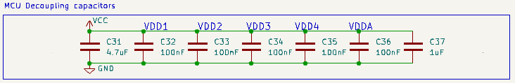
Figure 2: MCU Decoupling Capacitors Schematic
Now a table with some information about each one of the PINs of thee MCU is given and most relevant explanations are provided later:
| Pin Number / Name | PCB Pin Name | Type | Description |
|---|---|---|---|
| 1/VBAT | VCC | Power | General Power line at 3.3V |
| 2/PC13 | NC | - | - |
| 3/PC14 | OSC32_IN | Input | 32 kHz Oscillator Input |
| 4/PC15 | OSC32_OUT | Output | 32 kHz Oscillator Output |
| 5/PHO | OSC_IN | Input | 12 MHz Oscillator Input |
| 6/PH1 | OSC_OUT | Output | 12 MHz Oscillator Output |
| 7/NRST | NRST | Digital Input | STM32 Reset Pin |
| 8/PC0 | SCL3 | I2C | I2C3 Clock Bus |
| 9/PC1 | SDA3 | I2C | I2C3 Data Bus |
| 10/PC2 | SEL_PH0 | Digital Output | Selector for Photodiode Multiplexer |
| 11/PC3 | NC | - | - |
| 12/VSSA | GND | Power | Ground |
| 13/VDDA | VCC | Power | General Power line at 3.3V |
| 14/PA0 | BATT_NTC | Analog Input | Battery Temperature NTC Sensor |
| 15/PA1 | ADC_PL | Analog Input | ADC Input |
| 16/PA2 | X | NC | Unused Pin for Future or No Use |
| 1/PA3 | CHRGOFF | Digital Output | Battery Charging Enable Pin |
| 18/VSS | GND | Power | Ground |
| 19/VDD | VCC | Power | General Power line at 3.3v |
| 20/PA4 | CLPROG | Analog Outpot | Charge Current Programming Output |
| 21/PA5 | DAC_PL | Analog Output | DAC Output for Payload |
| 22/PA6 | X | Not connected | Unused Pin for Future or No Use |
| 23/PA7 | PoL_ADCS_POWER_EN | Digital Output | Point of Load Control for ADCS |
| 24/PC4 | FAULT | Digital Input | Battery Charging Fault Status Pin |
| 25/PC5 | ADC_PH | Analog Input | Photodiode Array Output |
| 26/PB0 | STM32_PB0 | GPIO | Connected to STM32 PB0, User Defined |
| 27/PB1 | X | Not connected | Unused Pin for Future Use |
| 28/PB2 | CHRG | Digital Input | Battery Charging Monitoring Pin |
| 29/PB10 | HEATER_EN | Digital Output | Heater Enable Pin |
| 30/PB11 | PoL_BURN_EN | Digital Output | Point of Load Control for Antenna Deployment |
| 31/VSS | GND | Power | Ground |
| 32/VDD | VCC | Power | General Power line at 3.3V |
| 33/PB12 | SX1262_NSS | SPI Chip Select | SX1262 Chip Select |
| 34/PB13 | SCK | SPI Clock | SX1262 SPI Clock |
| 35/PB14 | MISO | SPI MISO | SX1262 SPI Master-In Slave-Out |
| 36/PB15 | MOSI | SPI MOSI | SX1262 SPI Master-Out Slave-In |
| 37/PC6 | PoL_P/L_EN | Digital Output | Point of Load Control for Payload |
| 38/PC7 | X | Not connected | Unused Pin for Future or No Use |
| 39/PC8 | X | Not connected | Unused Pin for Future or No Use |
| 40/PC9 | SX1262_NRST | Digital Input | SX1262 Reset |
| 41/PA8 | SX1262_BUSY | Digital Ouput | SX1262 Busy Indicator |
| 42/PA9 | STM32_PA9 | GPIO | Connected to STM32 PA9, User Defined |
| 43/PA10 | DIO1 | Digital Iinput | SX1262 Interrupts |
| 44/PA11 | SEL_PH1 | Digital Output | Selector for Photodiode Multiplexer |
| 45/PA12 | SEL_PH2 | Digital Output | Selector for Photodiode Multiplexer |
| 46/PA13 | SWDIO | Serial Wire I/O | STM32 Debug Port |
| 47/VSS | GND | Power | Ground |
| 48/VDDUSB | VCC | Power | General Power line at 3.3V |
| 49/PA14 | SWCLK | Serial Wire | STM32 Debug Port |
| 50 /PA15 | STM32_PA15 | GPIO | Connected to STM32 PA15, User Defined |
| 51/PC10 | UART_TX | UART (Output) | UART TX Bus to P/L |
| 52/PC11 | UART_RX | UART (Input) | UART RX Bus to P/L |
| 53/PC12 | X | Not connected | Unused Pin for Future or No Use |
| 54/PD2 | X | Not connected | Unused Pin for Future or No Use |
| 55/PB3 | SWO | Serial Wire | STM32 Debug Pin |
| 56/PB4 | X | Not connected | Unused Pin for Future or No Use |
| 57/PB5 | PFO | Power | Power Fault Output |
| 58/PB6 | SCL1 | I2C | I2C1 Clock Bus |
| 59/PB7 | SDA1 | I2C | I2C1 Data Bus |
| 60/BOOT0 | Boot0 | Boot | Boot Pin |
| 61/PB8 | X | Not connected | Unused Pin for Future or No Use |
| 62/PB9 | X | Not connected | Unused Pin for Future or No Use |
| 63/VSS | GND | Power | Ground |
| 64/VDD | VCC | Power | General Power line at 3.3V |
Table 3: MCU PINs
The Point-of-Load (PoL) control provides powering of critical components of the system, those being the P/L, ADCS, Thermal Knife and the Battery Heater. The IC is powered by the 3.3V line and the schematic follows the manufacturers reference design, with EN/EN# pin being controlled by the OBC with GPIOs (as MCU Outputs).
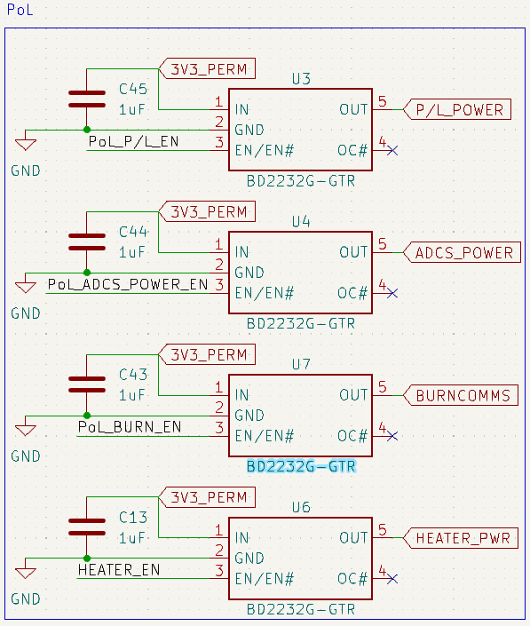
Figure 3: PoL Controls Schematic
The outputs of these PoL is connected to the vertical connectors on the sides of the PCB.
The OBC external clocks are provided with decoupling capacitors to minimize any noise that might affect the reference signals. The schematics are provided next:
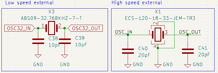
Figure 3: External Clocks Schematic
Capacitors are placed at the extremes of the clocks to reduce the gain of higher harmonics produced by the crystals themselves.
A schematic of the whole system is provided now, highlihting the parts with different colours:

Figure 4: Overall OBC Schematic
Next an explanation of the OBC side of the OBC-COMMS PCB is given. Information related to the COMMS side is in its respective section. A render of the PCB is provided in the next figure:
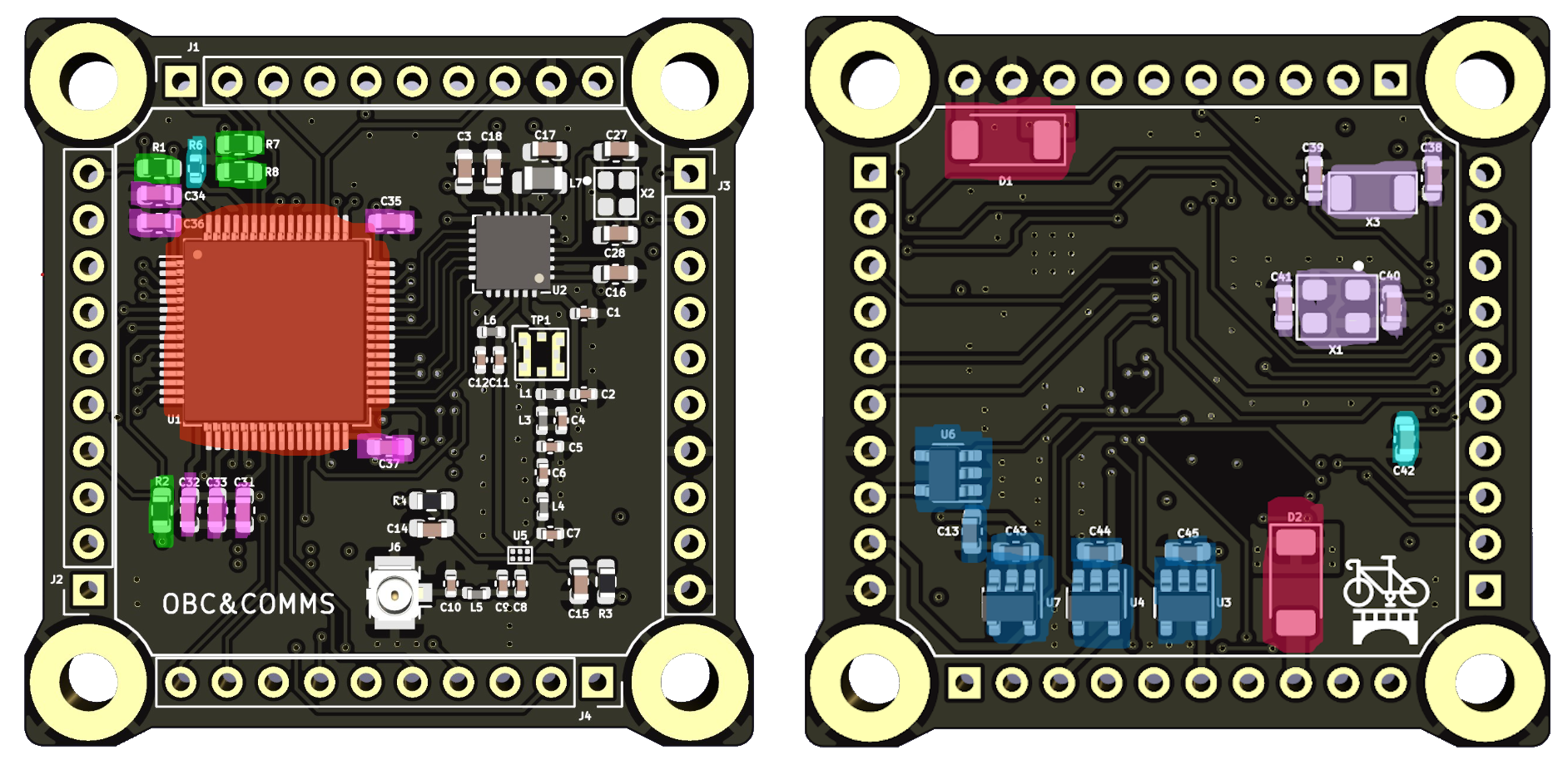
Figure 5: OBC-COMMS PCB with OBC Components highlighted
The MCU is located at the top layer of the PCB, placed at the left side of the board to keeking most power distribution as far away as possible from the COMMS side of the PCB to minimize interference. This distribution also keeps the I2C pins close to the vertical connectors which helps reduce noise from the PCB. The Decoupling capactitors are placed throughout the board on the STM32 voltage pins.
The I2C Pull-up resistors are simply placed as close as possible to the corresponding pins. This decision also happens to minimize the lenght of the lines as the PINs are close to the vertical conectors. This same philosophy applies to the input capacitor and resistor for NRST and Boot0.
All this components are besides the NRST capacitor are on the top layer. On the bottom layer we find the Power switch ICs (PoL Control) which are once again located as close as possible to the vertical connectors where their outputs match in order to minime power losses, keep lines short and avoid interferences with COMMS. On the same side are the Crystal oscillators which are located at the top right corner as the MCU is then located straight on top of them. This is fundamental as the harmonics generated by these clocks are dangerous to the COMMS subsystem, so keeping them as far as possible from the RF lines and transciever minimizes risk of coupling.
The last piece of the OBC PCB are the Umbilical diode and connector, also on the bottom layer and, once again, close to the vertical connectors for the same reasons as before.
A list of the components as well as some information for each part is provided next:
The table containing the MCU information:
| Characteristic | Description |
|---|---|
| Microcontroller | STM32L476RGT7 |
| MCU Manufacturer | ST |
| Core | ARM Cortex M4 |
| Word Length | 32-bit |
| Frequency (MHz) | 80 |
| Architecture | RISC |
| FPU | Yes |
| Consumption | 9.6mA |
| Interfaces | x3 I2C, x3 SPI, x2 UART, x3 USART, x8 GPIO |
| ADC | 3 |
| DAC | 2 |
| Flash | 1MB |
| RAM | 128KB |
Table 4: MCU Information
Capacitor C31 is a 4.7uF ceramic capacitor (GRT188R61E475KE13D) with the following characteristics:
| Temp. coeff. or Cap. Change | Temp. Range | Ref. Temp. | Rated Voltage | Capacitance | Capacitance Tolerance | Operating Temp. Range | Mounting Method |
|---|---|---|---|---|---|---|---|
| -15 to 15 % | -55 to 125°C | 25°C | DC 100V | 4.7uF | +/-10% | -55 to 85°C | Flow, Reflow |
Table 5: GRT188R61E475KE13D (C31) Relevant Values
Capacitors C32 to C36 are all 100nF ceramic capacitors (GRM188R72A104KA35J) with the following characteristics:
| Temp. coeff. or Cap. Change | Temp. Range | Ref. Temp. | Rated Voltage | Capacitance | Capacitance Tolerance | Operating Temp. Range | Mounting Method |
|---|---|---|---|---|---|---|---|
| -15 to 15 % | -55 to 125°C | 25°C | DC 100V | 0.1uF | +/-10% | -55 to 125°C | Flow, Reflow |
Table 6: GRM188R72A104KA35J (C32, C33, C34, C35, C36) Relevant Values
Capacitor C37 is a 1uF ceramic capacitor (GRM188R61A105KA61D) with the following characteristics:
| Temp. coeff. or Cap. Change | Temp. Range | Ref. Temp. | Rated Voltage | Capacitance | Capacitance Tolerance | Operating Temp. Range | Mounting Method |
|---|---|---|---|---|---|---|---|
| -15 to 15 % | -55 to 85°C | 25°C | DC 10V | 1uF | +/-10% | -55 to 85°C | Flow, Reflow |
Table 7: GRM188R61A105KA61D (C37) Relevant Values
The I2C PU Resistors (R1, R2, R7, R8) are all 4.7k thick film resistors (CRCW06034K70JNEAC):
| Resistance | Power Rating | Tolerance | Temp. Coefficient | Min. Operating Temp. | Max. Operating Temp. | Voltage Rating |
|---|---|---|---|---|---|---|
| 4.7 kOhms | 100 mW (1/10 W) | 5% | 200 PPM / °C | -55 °C | +155 °C | 75 V |
Table 8: I2C PU Resistors Values (R1, R2, R7, R8)
The Crystal oscillators present the following capacitors to filter harmonics:
| RefDes | Package | Value | Qty | Description | Manufacturer Code |
|---|---|---|---|---|---|
| C38, C39 | 0402 | 10pF | 1 | Multilayer ceramic capacitors C0G ±2%, 50V | 06035A100GAT2A |
| C40, C41 | 0402 | 3.3pF | 1 | Multilayer Ceramic Capacitors C0G ±5%, 100V | GCM1885C2A200JA16D |
Table 9: Crystal Oscillators Capacitors Values
The umbilical connector boasts two diodes, which are the same component:
| Type | Configuration | Technology | If | Vrrm | Vf | Ifsm | Ir | Vr | Max Op. Temp. |
|---|---|---|---|---|---|---|---|---|---|
| Schottky Diodes | Single | Si | 1 A | 40 V | 340 mV | 40 A | 150 µA | 20 V | +125 °C |
Table 10: Umbilical Diodes Values
NRST and Boot0 make use of the following components:
| Resistance | Power Rating | Tolerance | Temp. Coefficient | Min. Operating Temp. | Max. Operating Temp. | Voltage Rating |
|---|---|---|---|---|---|---|
| 10 kOhms | 63 mW (1/16 W) | 1% | 100 PPM / °C | -55 °C | +155 °C | 50 V |
Table 11: R6 Values
The power switch capacitors are the same as the C37 decoupling capacitor .
The OBC-COMMS layers are explained on the COMMS section of hardware-
The Due to the novel nature of the satellite, research in this area is somewhat restricted. Most of the currently deployed spacecraft are primarily the outcome of educational initiatives and an emerging market. Considering all this, the assessment is focused on three enterprises currently offering market solutions, the already introduced Alba Orbital and FOSSA Systems, along with Citadel Space Systems. It is worth mentioning that the products of the latter company, still do not have experience in space. The 3 reference PocketQubes are Unicorn-2, FOSSASat-2 and Scquire, developed by Alba Orbital, FOSSA Systems and, Citadel Space Systems respectively.
The analysis breakdown of their microcontrollers on-board is performed in table 2.1. The underlying purpose of this comparison is to identify the technology that best meets the requirements of our On-Board Computer. In this regard, the research is focused on the relevant features of the microcontroller selected to fly towards space, such as word length, maximum frequency, architecture among others.
| Organization | Alba Orbital | FOSSA Systems | Citadel Space Systems |
|---|---|---|---|
| PocketQube | Unicorn-2 | FOSSASat-2 | Squire |
| Microcontroller | MSP430 | STM32L4 | TMS570 |
| MCU Manufacturer | TI | ST | TI |
| Core | CPU | ARM Cortex M4 | ARM Cortex R5F |
| Word Length | 16-bit | 32-bit | 32-bit |
| Frequency (MHz) | 16 | 80 | 300 |
| Architecture | RISC | RISC | RISC |
| FPU | No | Yes | Yes |
| Consumption | 6.72mA | 9.6mA | 990mA |
| Interfaces | x1 I2C, x1 SPI, x1 UART | x3 I2C, x3 SPI, x2 UART, x3 USART, x8 GPIO | x2 I2C, x5 SPI, x4 UART, x16 GPIO |
| ADC | 8 | 3 | 2 |
| DAC | - | 2 | - |
| Flash | 16KB | 1MB | 4MB |
| RAM | 512B | 128KB | 512KB |
Table x: State of the art comparison
According to the previous table, the microcontroller selected by the emergent picosatellite companies are Texas Instruments (TI) and STMicroelectronics (ST). Regarding the processor core, it is common for the microcontrollers to be based upon a processor manufactured by another enterprise. In this case, the STM32L4 and the TMS570 are based on ARM Cortex M4 and ARM Cortex R5F respectively, both developed by Arm. However, TI has opted to develop the Central Processing Unit (CPU) core themselves. Furthermore, the critical features that significantly impact microcontroller per-On-board computer software development for PocketQubes formance are frequency and word length.
On the one hand, the frequency establishes the speed of the CPU, expressed in Hertz or MegaHertz represents the number of clock cycles per second. In our scenario, the TMS570 is the fastest in terms of intruction execution with 300 MHz, followed by the STM32L4 with 80 MHz and finally, the slowest being MSP430 at 16 MHz. On the other hand, the word length determines the width of the processor registers and the bus data width. Consequently, the memory space, data and instruction handling, and data precision are dependent on this parameter. For this reason, the processing performance of the 32-bit microcontroller from FOSSA Systems and Citadel Space Systems is more powerful, than the 16-bit selected by Alba Orbital.
However, performance comes together with power consumption so adjusting the system functioning to its requirements is key. In this context, the assessment should focus on the optimum trade-off between performance and power consumption where the battery capacity plays a critical role. The only parameter that the application writer can tune in order to regulate the power consumption is the clock frequency. For the sake of simplicity, the maximum power consumption of each microcontroller has been analyzed at their respective maximum frequencies (16 MHz, 80 MHz, and 300 MHz). As anticipated, the microcontroller operating at the highest frequency exhibits the highest power consumption, measuring 990 mA. This value is over ten times larger than the power consumption of the STM32L4, which consumes 9.6 mA, and the STM32L4, in turn, consumes twice the power of the MSP430 at 6.72 mA.
Furthermore, the system can reap advantages from the inclusion of a Floating Point Unit (FPU), which is specifically designed to handle floating-point operations. While the CPU is capable of performing such operations, the FPU executes them not only faster, but also with higher precision. Interestingly, Alba Orbital made the decision not to incorporate this component, whereas FOSSA Systems and Citadel Space Systems opted to implement it.
One thing in common among the pioneering entities is the architecture of the MCU. Based on Reduced Instruction Set Computing (RISC), the processing focuses on the use of simple instructions that can be executed in a clock cycle. In general, RISC architecture when compared to Complex Instruction Set Computing (CISC), is much faster, less resource consuming and more power-efficient, which is ideal for embedded systems. Even though CISC reduces the number of memory access since more operations can be done with a single complex instruction, pipelining in RISC also accelerates the memory access process.
Regarding interfaces, it is the part that depends the most on the overall system architecture. In other words, it depends on which are the devices that the microcontroller has to communicate with and which is the protocol required to do so. The system governing FOSSASAT-2 and Squire is more complex since they feature a wide variety of serial peripheral interfaces such as I2C, SPI, UART, USART and GPIO. On the contrary, Unicorn-2 looks somewhat simpler with only one I2C, one SPI and one UART peripheral interfaces required. In addition, FOSSASat-2 accomodates three ADCs, Scquire features two of them and MSP430 has up to 8 ADC channel available. In terms of DAC, STM32L4 is the only one having this feature, with 2 DACs.
Last but not least, the discussion concerning memory storage is given. As stated before it is directly dependent on the word length, since the more addresses we can use the larger the memory can be. Memory needs to have enough room for both data and the program itself. The three introduced PocketQubes accomodate a Flash memory along with a RAM memory whose sizes are determined according to the system needs.
# Software Design ## Overview As introduced in the previous sections, the On-board Computer (OBC) is responsible for governing the entire spacecraft. Since only one microcontroller is used to control the various subsystems and GPIOs, it is crucial to ensure efficient and robust performance of the PocketQube. The primary purpose of the OBC is to manage the housekeeping of the overall satellite, which includes timely data processing and storage while maintaining low power consumption. In this context, the Flight Software (FSW) running on the OBC must be carefully designed to meet the timing requirements associated with the diverse tasks the satellite is expected to perform. A common technique used in embedded systems to address these timing constraints is the implementation of Real-Time Operating Systems (RTOS). For the PocketQube, FreeRTOS has been selected as the open-source RTOS to manage the on-board FSW. For a better understanding of this section, it is recommended to read and comprehend the "[A Hands-On Tutorial Guide](https://www.freertos.org/Documentation/02-Kernel/07-Books-and-manual/01-RTOS_book)" provided by FreeRTOS beforehand, especially the sections on Task Management, Memory Management, Task Notifications, Event Groups, Queues, and Software Timers. ## OBSW Architecture The OBSW Architercure is designed with the purpose of performing the housekeeping of the overall satellite. In order to meet the time requirements linked to the varied tasks that the satellite is expected to perform, a Real time operating system (RTOS) is implemented. This RTOS allows task scheduling, crucial in our system with only one core, as well as inter-task communication and other functionalities. Considering the time and human limitations, as the Lektron team is comprised by students, the OBSW makes use of the Hardware Abstraction Layer provided by STM for their microcontrollers. This Hardware Abstraction Layer (HAL) simplifies the control of the Microcontroller Unit (MCU) interfaces greatly, reducing the amount of lower-level coding requiered by the programming user. Do note that to make full use of such libraries parts of it have been modified slightly for them to be FreeRTOS compatible. On the other hand drivers provided by Semtech are used to control the SX1262 Transciver. With the use of the aforementioned libraries, user functions and FreeRTOS tasks are designed and implemented in order to perform the specific mission requirements and tasks such as power management, telecommand processing and command, on-board data handling, payload data acquisition, attitude and orbit determination and control, between others. All user code is embedded into FreeRTOS tasks. Such code will make use of HAL and other libraries as well as the basic functions and methods of the C language in order. A simple diagram of this architecture is provided next: ](https://wiki.nanosatlab.space/uploads/images/gallery/2024-11/scaled-1680-/image-1731576596035.png)
Figure 2: Blocking data polling diagram
](https://wiki.nanosatlab.space/uploads/images/gallery/2024-11/scaled-1680-/image-1731576596035.png)
Figure 2: Blocking data polling diagram
The aim of this document is to clearly explain the tests performed during the delevolpment of the subsystem.
This document is based on current but also previous versions both of hardware and software and as such be followed with care.
The aim of this test is to verify that non of the components or connections had been damaging during the assembling, and that the consumption of the components is nominal.
| Requirement ID | Description |
|---|---|
| OBC-001 | There must be no visible damage to the board, such as scratches, soldering or joint issues. |
| OBC-011 | Each pin found in the lateral sides must have good electrical connection |
| OBC-012 | Verify that there are not any shorts, nor open ends, and the corresponding behavior and value |
| OBC-021 | The board must be powered with 3.3 V and all the power pins from the board must be checked |
| OBC-031 | All the other pins from the board must be electrically checked in order to make sure that the board is responding correctly |
The PCB will be verified if the five requirements mentioned before are fulfilled. If in one of them it is detected any anomaly it will have to be corrected, otherwise the board can not pass to the other tests.
The test for the EPS PCB has been done during the 01/06/2023.
The test passed the visual inspection since the outer physical checking was successful.
The pins', passive and active components' connectivity were successfully accomplished considering that there were no open ends or shorts, and the component values were correct.
The in-circuit testing was passed since the connections between all of the components and pints of the PCB were verified.
During the examination of the PCB no anomalies were detected.
The PCB passed the electrical test and is ready to do more complex tests.
The objective of this test is to verify that when providing the PCB with the power supply, the voltages and currents are correct on the whole PCB
The voltages required for each component are summarized in the following chart (they can be seen from the datasheet of each component):
| COMPONENT | Vin Min (V) | Vin Max (V) | Vo Min (V) | Vo Max(V) |
| SX1262IMLTRT | 1.8 | 3.7 | - | - |
| BGS12PL6E6327XTSA1 | 1.65 | 3.6 | - | - |
| STM32L476RGTx | 1.71 | 3.6 | - | - |
| BD2232G-GTR | 2.7 | 5.5 | -0.3 | Vin + 0.3 |
This test will be verified if the voltage obtained in the measurements of each component of the PCB is between the expected values.

With the help of the multimeter, check the voltage levels in the input and output of each component of the 3.2 chart
(the previous mentioned components are shown in order in the figures below, where the input put are marked in red)


This test for the EPS PCB has been done during the 01/06/2023.
| COMPONENT | Vin (V) |
| SX1262IMLTRT | 3.35 |
| BGS12PL6E6327XTSA1 | 3.32 |
| STM32L476RGTx | 3.27 |
| BD2232G-GTR | 3.34 |
As it can be seen in the previous chart, all the components have the correct input voltage. The test has been correctly passed.
No anomalies has been detected
The PCB passed the test and is ready to do more complex tests.
The objective of this test is to verify that it is possible to flash code to the STM32L476RG using the ST-Link v2
| Requirement ID | Description |
|---|---|
|
OBC-101 |
The program ST-Link Utility must detect the STM32L476RG |
|
OBC-111 |
The STM32 must be able to run code |
|
OBC-121 |
A very simple instruction with a visible result must be written in order to prove that the code works correctly |
This test will be verified if the two requirements are fullfiled.


ST-Link V2 connected to PC?
Yes
Connections ok? Revise ST-Link V2 and STM32 custom board SWD connections
Connection ok** **
**

STM32CubeIDE debbuger configured ok?

Supply ok? Check voltages
ST-Link V2 ok? Try programming Nucleo board with ST-Link V2d
STM32 detects the nucleo board. Therefore, the ST_Link v2 is ok.

Signals and logic ok? Connect Saleae to SWD and NRST in STM32 custom board
The SWDO and the SWCLK are working ok, but no signal is received from the NRST PIN. The same happens when the Saleae is connected directly to the STM32.
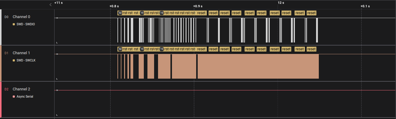
Signals from ST-Link V2 ok? Connect Saleae to SWD and NRST in ST-Link V2. Check if NRST is being aserted
Prepare STM32 board with minimum connections, only supply, gnd and SWD, does it work?
No, the ST-Link still does not detect the STM32
Resolder the board
When resoldering the board a mistake was detected: The STM32 has two orientation marks, and it was placed in the wrong direction. It is important to know that the hole that indicates the direction of the STM32 is the small one:

With the STM32 well orientated and the new PCB resoldered, the ST-Link can now make a connection with the STM32L476RG and flash code into it.
This test for the OBC PCB has been done during the 02/06/2023.
The STM32L476RG was succesfully detected by the ST-Link Utility program

The STM32CubeIde also detected the STM32 and was able to run code through it.

When trying to do the connection with the ST-Link utility program, the STM32 was no detected. The debugging process realized to solve this problem can be seen in 4.5.1.
The PCB passed the test.
The aim of this test is to verify that the required functions of the OBC can be performed by the STM32L4 integrated.
| Requirement ID | Description |
|---|---|
|
OBC - 211 |
The peripherals must be able to be correctly initialized |
|
OBC - 212 |
The clock has been able to be configured |
|
OBC - 221 |
FreeRTOS must be able to create a task |
|
OBC - 222 |
FreeRTOS must be able to do task scheduling |
|
OBC - 223 |
FreeRTOS must be able to make queue inter-tasks communication |
|
OBC - 224 |
It is needed to write on memory flash |
|
OBC - 225 |
The clock configuration can be changed during run-time |
|
OBC - 231 |
Be able to do software timers triggering (in 80, 26, 8 and 2 MHz) |
The PCB will be verified if the five requirements mentioned before are fulfilled. If in one of them it is detected any anomaly it will have to be corrected, otherwise the board can not pass to the other tests.
The test for the OBC PCB has been done during the 10/06/2023.
All the requirements have been successfully met.
During the examination of the PCB no anomalies were detected.
The PCB passed the STM32 functional test.
This test is designed to attempt communication from the OBC-COMMS board, via I2C, to the TCN75A temperature sensor located on all of the lateral boards.
| Requirement ID | Description |
|---|---|
|
OBC-311 |
The sensor must be powered using the Nucleo board's output. |
|
OBC-312 |
Using the Nucleo, the configuration register of the temperature sensor must be set (TX). |
|
OBC-313 |
Using the Nucleo, the temperature data from the sensor must be received and tracked using PuTTY for a cleaner reading of the data (RX). |
|
OBC-321 |
The sensor must be powered using the output from the ST-Link/V2 programmer. |
|
OBC-322 |
The already written and tested code from the Nucleo must be correctly flashed onto the OBC-COMMS board using the ST-Link/V2 programmer. |
|
OBC-323 |
Using the OBC-COMMS board, the configuration register of the sensor must be set (TX). |
|
OBC-324 |
Using the OBC-COMMS board, the temperature data from the sensor must be received (RX). |
|
OBC-331 |
The temperature reading function must be defined and integrated in the main code from GitHub. |
|
OBC-332 |
The complete GitHub code, including the newly written function, must be flashed onto the OBC-COMMS board using the ST-Link/V2 programmer. |
|
OBC-333 |
Using the already flashed OBC-COMMS board, it must be shown that the configuration and temperature data is still being sent and received through I2C when the previously integrated function is called in the main(). |
Necessary materials:
The setup for the initial test with the Nucleo:

[Detailed schematic made in photoshop to be inserted at a later date]
The setup for the subsequent test with the OBC-COMMS board:

[Detailed schematic made in photoshop to be inserted at a later date]
All of the requirements mentioned before must be fulfilled. If any one of them is not satisfactorily carried out, the anomalies must be taken care of. This test is absolutely critical since this is the easiest peripheral for I2C communication testing and this protocol is used for most internal communication jobs, so it is mandatory that it works without a hitch.
Step 1:
Build the previously shown setup. Make sure all of the connections are good and, using the multimeter, measure all of the relevant voltages (Power Pin, NRST, SWDIO, SWCLK, I2C SDA, I2C SCL) to make sure they reach around 3.3 V.
Step 2:
All code and software related stuff will be done in STM32CubeIDE, as it's the easiest and most reliable tools to use.
Write code for transmitting configuration settings to the configuration register of the sensor (thus testing TX) and receiving temperature data from the temperature register of the sensor (thus also testing RX).
Make sure you read the documentation data for the TCN75A sensor in particular, how it handles I2C communication and pay special attention to the way the address of the sensor is formatted, taking into account the particular configuration of resistors from the lateral board which define the last 3 bits of said address.
Step 3:
Flash the Nucleo board with the code you have written (look-up tutorial), open PuTTY, put in the parameters of your serial virtual COM port which gets created automatically from the Nucleo debugger (you can see it in Device Manager -> Port) and connect. Run the program and see if the data gets transmitted correctly. You can touch the sensor to warm it up and check if the temperature readings match.
Optional:
You can check the I2C SDA and SCL signals respectively with the oscilloscope/Picoscope you're using.
The Picoscope IDE also allows you to decode the 2 signals if both are connected, which should technically give you the same output as in PuTTY.
Once you have made sure that you can communicate through I2C between the Nucleo board and the sensor, it's time to try it with the main OBC-COMMS board.
The steps you should follow are exactly the same:
Step 1:
Build the previously shown setup.
Step 2 (extremely important):
Create a new project and redo the pin configuration in order to match the KiCad project for the OBC-COMMS board.
In particular, the I2C pins are not PB8 and PB9, but PB6 and PB7.
The code until and including the main() can be copy-pasted in its entirety from the other project.
Step 3:
Flash the code from this new project on the OBC-COMMS board using the debugger and test the values for the relevant variables while debugging. Since the ST-Link/V2 does not create a virtual COM port, the easiest way to check if the I2C communication is correctly being performed is by debugging step by step and checking if the variables change according to how they're supposed to.
Now that the OBC-COMMS -> Temperature Sensor communication works, the only thing left to do is to create a function, integrate it in the full code and test its functionality as a whole.
One of the ways to do this is:
Step 1:
Decide in what subsystem you want to integrate this code. In this case, it would make the most sense to write a function in the ADCS subsystem, since everything related to the lateral board "depends" on the ADCS.
Step 2:
Write the function and its corresponding header. Make sure to include everything you need in the header, especially all files which contain the I2C functions.
The .c file will be basically the same as the other code, containing all the functions that the other one contains, and changing it so that the main() of the existing code is all contained inside a function that will be called in the main.c file in order to test if everything works as intended.
Step 3:
Call the previously brought up function in the main.c file of the program.
Repeat the setup from the previous test and flash the entire code on the OBC-COMMS board. While debugging, go step by step and when you reach the temperature sensor data reading function, click on "Step into", and again, go step by step and check the relevant variables to see if their values correspond with your expected outputs.
If everything is good and nothing in the code crashed unexpectedly, that means that the integration test was successful.
This is the code I wrote for the Nucleo board test (not including the autogenerated functions):
//* Includes ------------------------------------------------------------------*/
#include "main.h"
#include "i2c.h"

/* Private includes ----------------------------------------------------------*/
#include <string.h>
#include <stdio.h>
#include <math.h>
/* Private typedef -----------------------------------------------------------*/
/* USER CODE BEGIN PTD */
/* USER CODE END PTD */

/* Private define ------------------------------------------------------------*/
#define TCN75_ADDR 0x4C // Change as per your hardware configuration
#define REG_CONFIG 0x01
#define REG_TEMP 0x00

/* USER CODE BEGIN PD */
/* USER CODE END PD */

/* Private macro -------------------------------------------------------------*/
/* USER CODE BEGIN PM */
/* USER CODE END PM */

/* Private variables ---------------------------------------------------------*/
I2C_HandleTypeDef hi2c1;
UART_HandleTypeDef huart2;

/* USER CODE BEGIN PV */
/* USER CODE END PV */

/* Private function prototypes -----------------------------------------------*/
void SystemClock_Config(void);
static void MX_GPIO_Init(void);
static void MX_USART2_UART_Init(void);
void MX_I2C1_Init(void);

/* USER CODE BEGIN PFP */
void I2C_ReInit(void);
HAL_StatusTypeDef I2C_CheckError(I2C_HandleTypeDef *hi2c, uint16_t DevAddress);
void I2C_BusReset(void);
void UART_Log(char *message);
/* USER CODE END PFP */

/* USER CODE BEGIN 0 */
void I2C_ReInit(void) {
    HAL_I2C_DeInit(&hi2c1);
    MX_I2C1_Init();
}

HAL_StatusTypeDef I2C_CheckError(I2C_HandleTypeDef *hi2c, uint16_t DevAddress) {
    if (HAL_I2C_IsDeviceReady(hi2c, DevAddress, 3, 1000) != HAL_OK) {
        uint32_t errorCode = HAL_I2C_GetError(hi2c);
        char errorMsg[64];
        sprintf(errorMsg, "I2C Error: 0x%lx\r\n", errorCode);
        UART_Log(errorMsg);
        I2C_ReInit();
        return HAL_ERROR;
    }
    return HAL_OK;
}

void I2C_BusReset(void) {
    GPIO_InitTypeDef GPIO_InitStruct = {0};
    HAL_I2C_DeInit(&hi2c1);
    GPIO_InitStruct.Pin = GPIO_PIN_9 | GPIO_PIN_8;
    GPIO_InitStruct.Mode = GPIO_MODE_OUTPUT_OD;
    GPIO_InitStruct.Pull = GPIO_NOPULL;
    GPIO_InitStruct.Speed = GPIO_SPEED_FREQ_HIGH;
    HAL_GPIO_Init(GPIOB, &GPIO_InitStruct);
    for (int i = 0; i < 9; i++) {
        HAL_GPIO_WritePin(GPIOB, GPIO_PIN_8, GPIO_PIN_SET);
        HAL_Delay(1);
        HAL_GPIO_WritePin(GPIOB, GPIO_PIN_8, GPIO_PIN_RESET);
        HAL_Delay(1);
    }
    MX_I2C1_Init();
}

void UART_Log(char *message) {
    HAL_UART_Transmit(&huart2, (uint8_t*)message, strlen(message), HAL_MAX_DELAY);
}

int main(void) {
     HAL_Init();
    SystemClock_Config();
    MX_GPIO_Init();
    MX_USART2_UART_Init();
    MX_I2C1_Init();

    while (1) {
        uint8_t buf[12];
        int8_t val_bfc;
        float val_afc = 0.0f;
        uint8_t auxbuf[12];
        char sign = ' ';

        buf[0] = REG_CONFIG;
        buf[1] = 0x60; // Example configuration value

        char AuxilMsg[64];
        sprintf(AuxilMsg, "While loop reset \r\n");
        HAL_UART_Transmit(&huart2, AuxilMsg , strlen(AuxilMsg), HAL_MAX_DELAY);

        if (I2C_CheckError(&hi2c1, TCN75_ADDR << 1) == HAL_OK) {

        	sprintf(AuxilMsg, "I2C OK \r\n");
        	HAL_UART_Transmit(&huart2, AuxilMsg , strlen(AuxilMsg), HAL_MAX_DELAY);

            HAL_I2C_Master_Transmit(&hi2c1, TCN75_ADDR << 1, buf, 2, HAL_MAX_DELAY);
            buf[0] = REG_TEMP;

            sprintf(AuxilMsg, "First transmission complete \r\n");
            HAL_UART_Transmit(&huart2, AuxilMsg , strlen(AuxilMsg), HAL_MAX_DELAY);

            HAL_I2C_Master_Transmit(&hi2c1, TCN75_ADDR << 1, buf, 1, HAL_MAX_DELAY);

            sprintf(AuxilMsg, "Second transmission complete \r\n");
            HAL_UART_Transmit(&huart2, AuxilMsg , strlen(AuxilMsg), HAL_MAX_DELAY);

            HAL_I2C_Master_Receive(&hi2c1, (TCN75_ADDR << 1) | 0x01, buf, 2, HAL_MAX_DELAY);

            sprintf(AuxilMsg, "Receiving complete \r\n");
            HAL_UART_Transmit(&huart2, AuxilMsg , strlen(AuxilMsg), HAL_MAX_DELAY);

            if(buf[0] >= 0x80)
            {sign = '-';
            auxbuf[0] = buf[0] - 0x80;
            auxbuf[1] = buf[1];
            }
            else
            {
            auxbuf[0] = buf[0];
            auxbuf[1] = buf[1];
            }

            val_bfc = (uint8_t) auxbuf[0];
            for (int i = 0; i < 8; ++i) {
                if (auxbuf[1] & (1 << i)) {
                    val_afc += 1 / pow(2, 8-i);
                }
            }

            val_afc *= 100;

            char tempMsg[64];
            sprintf(tempMsg, "Temperature: %c%d.%02d C\r\n", sign, val_bfc, (int)val_afc);
            HAL_UART_Transmit(&huart2, (uint8_t*)tempMsg, strlen(tempMsg), HAL_MAX_DELAY);
        } else {
              UART_Log("I2C Error. Resetting...\r\n");
            I2C_BusReset();
        }

        HAL_Delay(500);
    }
}
And this is the specially created "i2c.h" file, which when the full integration test will be done will be placed in the "CommonResources" folder:
/*
 * Created on: 02.12.2023
 * Author: Vladimir Frunza
 */

/* Define to prevent recursive inclusion -------------------------------------*/
#ifndef __I2C_H
#define __I2C_H

#ifdef __cplusplus
extern "C" {
#endif

/* Includes ------------------------------------------------------------------*/
#include "stm32l4xx_hal.h"

/* USER CODE BEGIN Includes */

/* USER CODE END Includes */

extern I2C_HandleTypeDef hi2c1;

/* USER CODE BEGIN Private defines */

/* USER CODE END Private defines */

void MX_I2C1_Init(void);

/* USER CODE BEGIN Prototypes */

/* USER CODE END Prototypes */

#ifdef __cplusplus
}
#endif
#endif /* __I2C_H */
Flashing it on the board with the complete setup and reading the output from PuTTY, it looks something like this:

-> This is the sensor just measuring the background temperature;

-> This is the sensor heating up as I touch it;

-> And this is the sensor cooling down as I stop touching it.
This test is considered a success.
As previously mentioned, it is extremely important to make sure that the pin configuration for each test is correct.
In our case, the difference between the Nucleo and the OBC-COMMS board is the location of the I2C pins:
The Nucleo uses pins PB9 and PB8 for I2C While the OBC-COMMS board uses pins PB7 and PB6 for I2C


Apart from this change, all the software (including the code) is exactly the same, since the 2 communicating devices (the MCU from the OBC-COMMS board and the temperature sensor) are identical.
Again, as previously mentioned, since the ST-Link/V2 doesn't create a virtual COM port, the easiest way to check is to check the relevant variables in the code by debugging step by step.
In my test, this looks like this:

The relevant values after going through the entire main() are val_bfc (value before the comma) and val_afc (value after the comma).
As you can see:
This test is also considered a success.
Once everything else is done, this should be the easiest part. The only worries should be:
From the code I wrote, this is the header for the .c file, both of which are contained in the ADCS subfolder:
/*
 * Created on: 02.12.2023
 * Author: Vladimir Frunza
 */

#ifndef __LATBOARD_TEMP_SENSOR_H
#define __LATBOARD_TEMP_SENSOR_H

#ifdef __cplusplus
extern "C" {
#endif

/* Includes ------------------------------------------------------------------*/
#include "stm32l4xx_hal.h"

/* Private includes ----------------------------------------------------------*/
/* USER CODE BEGIN Includes */
#include "i2c.h"
#include "main.h"
/* USER CODE END Includes */

/* Private defines -----------------------------------------------------------*/
#define TCN75_ADDR 0x4C
#define REG_CONFIG 0x01
#define REG_TEMP 0x00
/* USER CODE BEGIN Private defines */

/* USER CODE END Private defines */

#ifdef __cplusplus
}
#endif

#endif /* __LATBOARD_TEMP_SENSOR_H */
And this is the .c file, named in the same way as the header, "latboard_temp_sensor":
/*
 * Created on: 02.12.2023
 * Author: Vladimir Frunza
 */

//* Includes ------------------------------------------------------------------*/
#include "latboard_temp_sensor.h"
#include "i2c.h"
#include "main.h"

/* Private includes ----------------------------------------------------------*/
#include <string.h>
#include <stdio.h>
#include <math.h>
/* Private typedef -----------------------------------------------------------*/
/* USER CODE BEGIN PTD */
/* USER CODE END PTD */

/* USER CODE BEGIN PFP */
void I2C_ReInit(void);
HAL_StatusTypeDef I2C_CheckError(I2C_HandleTypeDef *hi2c, uint16_t DevAddress);
void I2C_BusReset(void);
void UART_Log(char *message);
/* USER CODE END PFP */

/* USER CODE BEGIN 0 */
void I2C_ReInit(void) {
    HAL_I2C_DeInit(&hi2c1);
    MX_I2C1_Init();
}

HAL_StatusTypeDef I2C_CheckError(I2C_HandleTypeDef *hi2c, uint16_t DevAddress) {
    if (HAL_I2C_IsDeviceReady(hi2c, DevAddress, 3, 1000) != HAL_OK) {
        uint32_t errorCode = HAL_I2C_GetError(hi2c);
        char errorMsg[64];
        sprintf(errorMsg, "I2C Error: 0x%lx\r\n", errorCode);
        UART_Log(errorMsg);
        I2C_ReInit();
        return HAL_ERROR;
    }
    return HAL_OK;
}

void I2C_BusReset(void) {
    GPIO_InitTypeDef GPIO_InitStruct = {0};
    HAL_I2C_DeInit(&hi2c1);
    GPIO_InitStruct.Pin = GPIO_PIN_9 | GPIO_PIN_8;
    GPIO_InitStruct.Mode = GPIO_MODE_OUTPUT_OD;
    GPIO_InitStruct.Pull = GPIO_NOPULL;
    GPIO_InitStruct.Speed = GPIO_SPEED_FREQ_HIGH;
    HAL_GPIO_Init(GPIOB, &GPIO_InitStruct);
    for (int i = 0; i < 9; i++) {
        HAL_GPIO_WritePin(GPIOB, GPIO_PIN_8, GPIO_PIN_SET);
        HAL_Delay(1);
        HAL_GPIO_WritePin(GPIOB, GPIO_PIN_8, GPIO_PIN_RESET);
        HAL_Delay(1);
    }
    MX_I2C1_Init();
}

void UART_Log(char *message) {
    HAL_UART_Transmit(&huart4, (uint8_t*)message, strlen(message), HAL_MAX_DELAY);
}

void Send_Latboard_Temp(void)
{
	uint8_t buf[12];
	int8_t val_bfc;
	float val_afc = 0.0f;
	uint8_t auxbuf[12];
	char sign = ' ';

	buf[0] = REG_CONFIG;
	buf[1] = 0x60;

	char AuxilMsg[64];
	//sprintf(AuxilMsg, "While loop reset \r\n");
	//HAL_UART_Transmit(&huart2, AuxilMsg , strlen(AuxilMsg), HAL_MAX_DELAY);

	if (I2C_CheckError(&hi2c1, TCN75_ADDR << 1) == HAL_OK) {

	     //sprintf(AuxilMsg, "I2C OK \r\n");
	     //HAL_UART_Transmit(&huart2, AuxilMsg , strlen(AuxilMsg), HAL_MAX_DELAY);

	     HAL_I2C_Master_Transmit(&hi2c1, TCN75_ADDR << 1, buf, 2, HAL_MAX_DELAY);
	     buf[0] = REG_TEMP;

	     //sprintf(AuxilMsg, "First transmission complete \r\n");
	     //HAL_UART_Transmit(&huart2, AuxilMsg , strlen(AuxilMsg), HAL_MAX_DELAY);

	     HAL_I2C_Master_Transmit(&hi2c1, TCN75_ADDR << 1, buf, 1, HAL_MAX_DELAY);

	     //sprintf(AuxilMsg, "Second transmission complete \r\n");
	     //HAL_UART_Transmit(&huart2, AuxilMsg , strlen(AuxilMsg), HAL_MAX_DELAY);

	     HAL_I2C_Master_Receive(&hi2c1, (TCN75_ADDR << 1) | 0x01, buf, 2, HAL_MAX_DELAY);

	     //sprintf(AuxilMsg, "Receiving complete \r\n");
	     //HAL_UART_Transmit(&huart2, AuxilMsg , strlen(AuxilMsg), HAL_MAX_DELAY);

	     if(buf[0] >= 0x80)
	     {sign = '-';
	     auxbuf[0] = buf[0] - 0x80;
	     auxbuf[1] = buf[1];
	     }
	     else
	     {
	     auxbuf[0] = buf[0];
	     auxbuf[1] = buf[1];
	     }

	     val_bfc = (uint8_t) auxbuf[0];
	     for (int i = 0; i < 8; ++i) {
	         if (auxbuf[1] & (1 << i)) {
	         val_afc += 1 / pow(2, 8-i);
	         }
	     }

	     val_afc *= 100;

	     char tempMsg[64];
	     //sprintf(tempMsg, "Temperature: %c%d.%02d C\r\n", sign, val_bfc, (int)val_afc);
	     //HAL_UART_Transmit(&huart2, (uint8_t*)tempMsg, strlen(tempMsg), HAL_MAX_DELAY);

	     }

	else {

	     //UART_Log("I2C Error. Resetting...\r\n");
	     I2C_BusReset();

	     }

}
As you can see, the function that will be called in the main.c file is "Send_Latboard_Temp()", function which is almost a one to tone copy of the while(1) loop from the int main() of the previous program.
After including the "latboard_temp_sensor.h" in the "adcs.h" file which is included in the "main.h" file and calling the previously mentioned function in int main() of main.c, by stepping into it after debugging we can see:

At the end of the execution of the function, the previously talked about val_bfc and val_afc have the values 22 and 56.25 respectively, meaning a temperature of 22.56 °C.
Considering that everything else after the end of the execution of this functions runs as it should, meaning all tasks and all timers are created correctly, we can say that this test is also a success, meaning the absolute goal was accomplished.
Making everything work for this test took considerably longer than expected, and here is a list of problems I faced that anyone who tries I2C communication should also consider and thoroughly verify:
1. Connection issues
Be it either cables being damaged, boards being improperly soldered, connectors not touching or any other one of these very common problems, I2C like any other communication protocol requires a strong and well defined signal, especially when trying to communicate something as delicate as an exact temperature value, where even a bit flip can have dramatic consequences.
The only real way to make sure that you're not experiencing any connection issues is to painstakingly check every possible connection by hand, firstly with a simple multimeter in order to make sure that your voltages are correct, and then with an oscilloscope in order to more finely analyze the signals transmitted.
Separating each connection and testing it individually is always better than trying to test everything when it's all connected, since there can be a lot of broken links in a bigger chain and it's way harder to identify which one is problematic.
2. Unfamiliar connectors
When working on any electronics project, you might very quickly come to see a component of any kind with which you are unfamiliar. In that case, instead of trying to work your way around a functionality of said component, it is always better to use it as it is intended, since that is the optimal way to make sure that you are not shooting yourself in the foot.
In our case, the lateral board has a 10/11 pin connector which requires special crimping of cables with a specialized Molex crimping tool in order for the connection to be strong. Trying without crimping has led quickly led me to the conclusion that, even though there might be a connection, for something like I2C a poor connection is as good as no connection.
3. Burned or damaged components
Every board that requires soldering is subject to damage: damage of the copper traces, damage of the lateral connectors, damage of the components, etc.
Sometimes it is better to make manually make sure that all your components are in working condition and that the connections between them are not damaged than just assume that's the case and have to suffer the potential consequences. Other times, changing them anyway might even be the safer strategy.
4. Mistakes in the basic setup of the experiment
Be it either a mistake in the physical setup, the setup in the IDE or even a big gap in the logic of the code itself, these mistakes are extremely common and do happen to everyone.
The only way to prevent this is to check even the things that you consider to be the most basic and logical things from the get go. Read all the documentation for the chips you are using, thoroughly consult all the schematics for the circuits that you are using and never assume that if something worked in a specific way with a board that it should work exactly the same with another one.
The I2C testing of the temperature sensor from the lateral boards was a complete success and now we can be sure that we have an OBC-COMMS board with working I2C pins that is ready for further testing of the peripherals.
The aim of this test is to verify that the OBC payload can establish a correct communication with the ADCS board and receive data from the gyroscope.
| Requirement ID | Description |
|---|---|
|
OBC-411 |
The ADCS board must be powered using the Nucleo board's output. |
|
OBC-412 |
Using the Nucleo, the I2C communication between the gyroscope and the MCU must be established, and the data must be correctly transmitted. |
|
OBC-421 |
The ADCS board must be powered using the ST-Link/V2 output. |
|
OBC-422 |
The ADCS board and the OBC board should be able to communicate data from the gyroscope to the MCU through I2C. |
|
OBC-431 |
The gyroscope reading function must be defined and integrated in the main code from GitHub. |
|
OBC-432 |
The complete GitHub code, including the newly written function, must be flashed onto the OBC-COMMS board using the ST-Link/V2 programmer. |
|
OBC-433 |
Using the already flashed OBC-COMMS board, it must be shown that the I2C communication between the chips still works when the previously integrated function is called in the main(). |
This is the list of required materials for this test:
The test will be verified if the requirements mentioned before are fulfilled. If in one of them it is detected any anomaly it will have to be corrected, otherwise the board can not pass to the other tests.
This is a picture of the setup for the Nucleo board test:

To complete this test, the following steps should be followed:
Step 1: Connect the 3.3V pin to the ADCS PCB.
Step 2: With the help of the multimeter, check that the VCC inputs pins has the correct value.
Step 3: Connect the Nucleo's SCL and SDA pins to the ADCS's corresponding I2C 3 pins.
Step 4: Prepare a code that can read from the gyroscope using I2C
Step 5: Run the code into the Nucleo and debug it step by step to see if the communication between the Nucleo and the ADCS has been done.
This is a picture of the setup:

These are the steps to follow:
Step 1: Connect the power supply from the ST-Link/V2 to the ADCS PCB and OBC PCB
Step 2: With the help of the multimeter, check that the VCC inputs pins has the correct value
Step 3: Connect the OBC payload to the computer using SWDIO pins
Step 4: Prepare a code that can read from the gyroscope using I2C
Step 5: Connect the OBC to the ADCS PCB using SCL and SDA pins
Step 6: Run the code into the OBC and look in the memory register to see if the communication between the OBC and the ADCS has been done.
This is the code used for the Nucleo - ADCS data read test:
/* Includes ------------------------------------------------------------------*/
#include "main.h"
#include "iim42652.h"
#include "Sumador.h"
#include <string.h>
#include <stdio.h>
#include <stdlib.h>

/* Private includes ----------------------------------------------------------*/
/* USER CODE BEGIN Includes */
int buf[100];
/* USER CODE END Includes */

/* Private typedef -----------------------------------------------------------*/
/* USER CODE BEGIN PTD */

/* USER CODE END PTD */

/* Private define ------------------------------------------------------------*/
/* USER CODE BEGIN PD */

/* USER CODE END PD */

/* Private macro -------------------------------------------------------------*/
/* USER CODE BEGIN PM */

/* USER CODE END PM */

/* Private variables ---------------------------------------------------------*/
I2C_HandleTypeDef hi2c1;

UART_HandleTypeDef huart2;

/* USER CODE BEGIN PV */

/* USER CODE END PV */

/* Private function prototypes -----------------------------------------------*/
void SystemClock_Config(void);
static void MX_GPIO_Init(void);
static void MX_USART2_UART_Init(void);
static void MX_I2C1_Init(void);
/* USER CODE BEGIN PFP */

/* USER CODE END PFP */

/* Private user code ---------------------------------------------------------*/
/* USER CODE BEGIN 0 */

/* USER CODE END 0 */

/**
  * @brief  The application entry point.
  * @retval int
  */
int main(void)
{
	/* USER CODE BEGIN 1 */
		uint8_t GyroState=1;
		uint8_t ValidData=1; // 1=true,0=false
	  /* USER CODE END 1 */

	  /* MCU Configuration--------------------------------------------------------*/

	  /* Reset of all peripherals, Initializes the Flash interface and the Systick. */
	  HAL_Init();

	  /* USER CODE BEGIN Init */

	  /* USER CODE END Init */

	  /* Configure the system clock */
	  SystemClock_Config();

	  /* USER CODE BEGIN SysInit */

	  /* USER CODE END SysInit */

	  /* Initialize all configured peripherals */
	  MX_GPIO_Init();
	  MX_USART2_UART_Init();
	  MX_I2C1_Init();
	  /* USER CODE BEGIN 2 */
	  IIM_init(&hi2c1);
	  IIM_configGyro(SET_GYRO_FS_SEL_15_625_dps, SET_GYRO_ODR_1kHz);

	  /* USER CODE END 2 */
	  //float degreesx=0,degreesz=0,degreesy=0,temperature=0;
	   iim_raw_data data;
	   iim_scaled_data scaled_data;
	   iim_averaged_data averaged_data;
	   CircularQueue queueX,queueY,queueZ;
	   int8_t average_samples=10;//10=1 seg
	   int counter=0,full=0; //full=1 databuffer full
	  /* Infinite loop */
	  /* USER CODE BEGIN WHILE */
	  int databuf_size=100;
	  float databuffer[databuf_size];
	  uint8_t capacity=queue_compute_capacity(0.1,1);
	  queue_init(&queueX,&queueY,&queueZ,capacity);
	  while (1)
	  {
	    /* USER CODE END WHILE */

	    /* USER CODE BEGIN 3 */
		  IIM_readGyro(&data);
		  IIM_convertGyro(&scaled_data,data,GyroState);
		  IIM_readTemperature(&data.temperature);D
		  IIM_ChangeState_Gyro(&data,&scaled_data,&GyroState,&ValidData);
		  HAL_Delay(100);
		  if(ValidData==1){
			  average_algorithm(&scaled_data,&averaged_data,&queueX,&queueY,&queueZ);
			  sprintf((char*)buf,"%d  %d  %d  %d \r\n",data.x,data.y,data.z,data.temperature);
			  HAL_UART_Transmit(&huart2, buf, strlen((char*)buf), HAL_MAX_DELAY);
		  }

	  }
  /* USER CODE END 3 */
}Unfortunately, the ADCS board I worked with could not correctly flash this code, since there were issues with the 2 I2C pins who constantly remained at 0 V.
Even though I have briefly tried to figure out what the problem could be, it seems like there are more things wrong with that board.
That being said, Edgar Hernandez Recio, the ADCS responsible who wrote the code from above, did manage to flash and correctly transmit gyroscope data through I2C with this code, using another board.
So, this test is a success, but it will need replicating if I want to test the OBC-COMMS -> ADCS communication, most likely with the only ADCS board that seems to work.
After I changed the ADCS board from the one that obviously wasn't working to Edgar's working board and working together with him in order to make sure that we have the correct software configuration inside the IDE (correct code + correct pinout), we managed to replicate the Nucleo board test with my laptop, resulting in a complete success of test 1.
After that, I changed the configuration to the one for the OBC-COMMS test, again worked with Edgar to ensure that everything is as intended, and managed to communicate through I2C between the OBC-COMMS board and the ADCS board, resulting in a complete success of test 2 and, by proxy, the entire experiment.
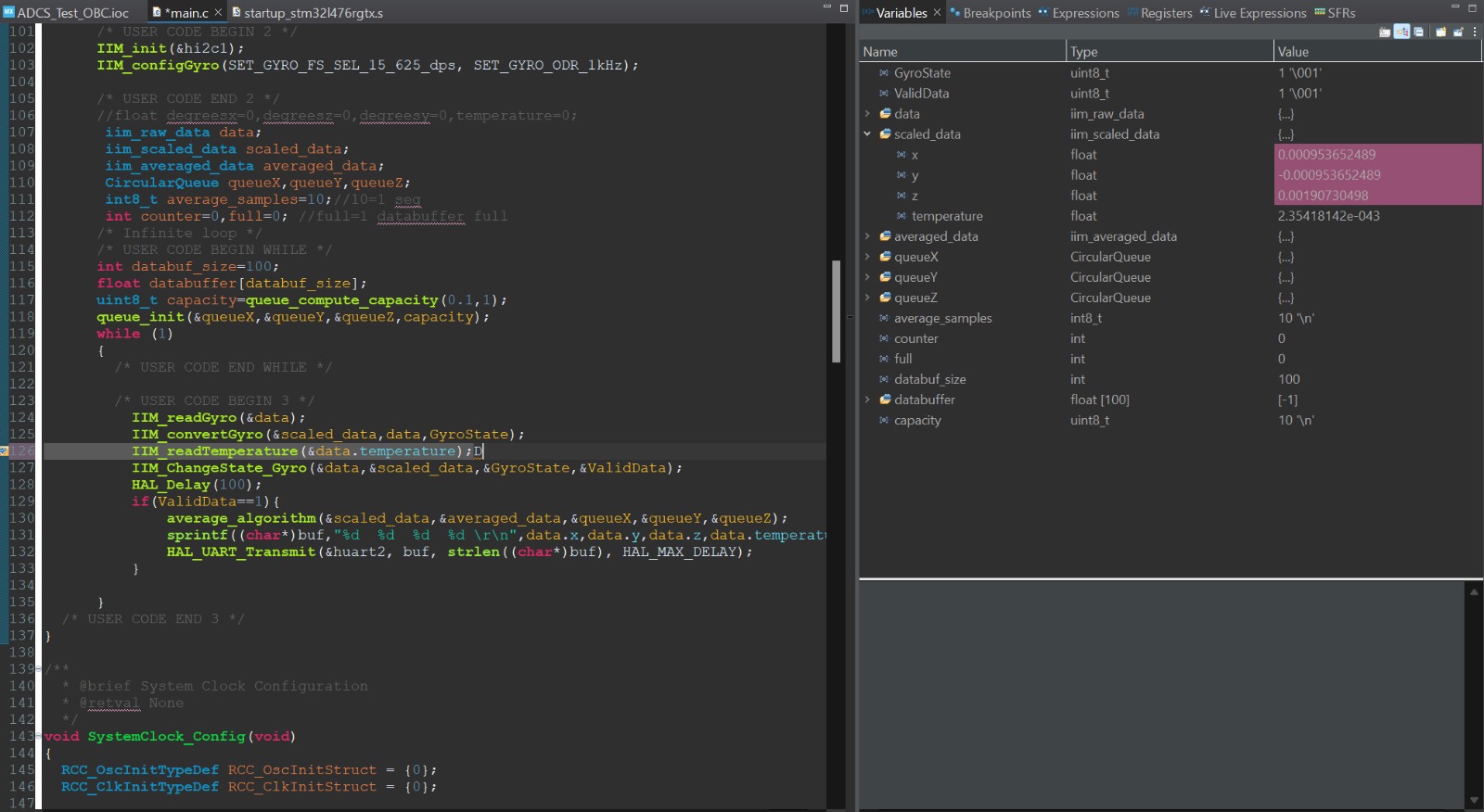
This is how a correct non-moving test with correct values is supposed to look. All of the 3 values from the 3 axis of the gyroscope are pretty much 0, indicating complete stillness.
The biggest anomaly that we faced is that only one of the ADCS boards we have is fully operational.
This could be due to many factors, some of the most likely culprits being:
In order to increase the efficiency of the workflow, the recommendable thing to do is fix at least one of the non-working ADCS boards, as to enable multiple people testing with ADCS at the same time. The best solution to doing this is to completely resolder new components from scratch, since that is the only way to ensure that everything will be working as intended.
The ADCS gyroscope data read test was a complete success, so that means that we can continue with the peripheral testing and also have the certainty that at least one ADCS board is fully operational.
The aim of this test is to verify that the OBC which was previously shown to be able to establish a correct communication with the ADCS board can also correctly read data from the photodiode, meaning that both the photodiode itself and the Analog to Digital Converter must work as intended.
| Requirement ID | Description |
|---|---|
|
OBC-511 |
The ADCS board and lateral board must be powered using the Nucleo board's output. |
|
OBC-512 |
Using the Nucleo, the I2C communication between the photodiode and the MCU must be established and the data must be correctly transmitted once it has been converted by the ADC. |
|
OBC-521 |
The ADCS board and lateral board must be powered using the ST-Link/V2 output. |
|
OBC-522 |
The ADCS board, the OBC board and the lateral board should be able to communicate data from the photodiode through I2C and the readable data correctly converted by the ADC. |
|
OBC-531 |
The photodiode reading function must be defined and integrated in the main code from GitHub. |
|
OBC-532 |
The complete GitHub code, including the newly written function, must be flashed onto the OBC-COMMS board using the ST-Link/V2 programmer. |
|
OBC-533 |
Using the already flashed OBC-COMMS board, it must be shown that the I2C communication between the chips still works when the previously integrated function is called in the main(). |
This is the list of required materials for this test:
The test will be verified if the requirements mentioned before are fulfilled. If in one of them it is detected any anomaly it will have to be corrected, otherwise the board can not pass to the other tests.
This is the picture of the necessary setup (and a cameo by Artur):
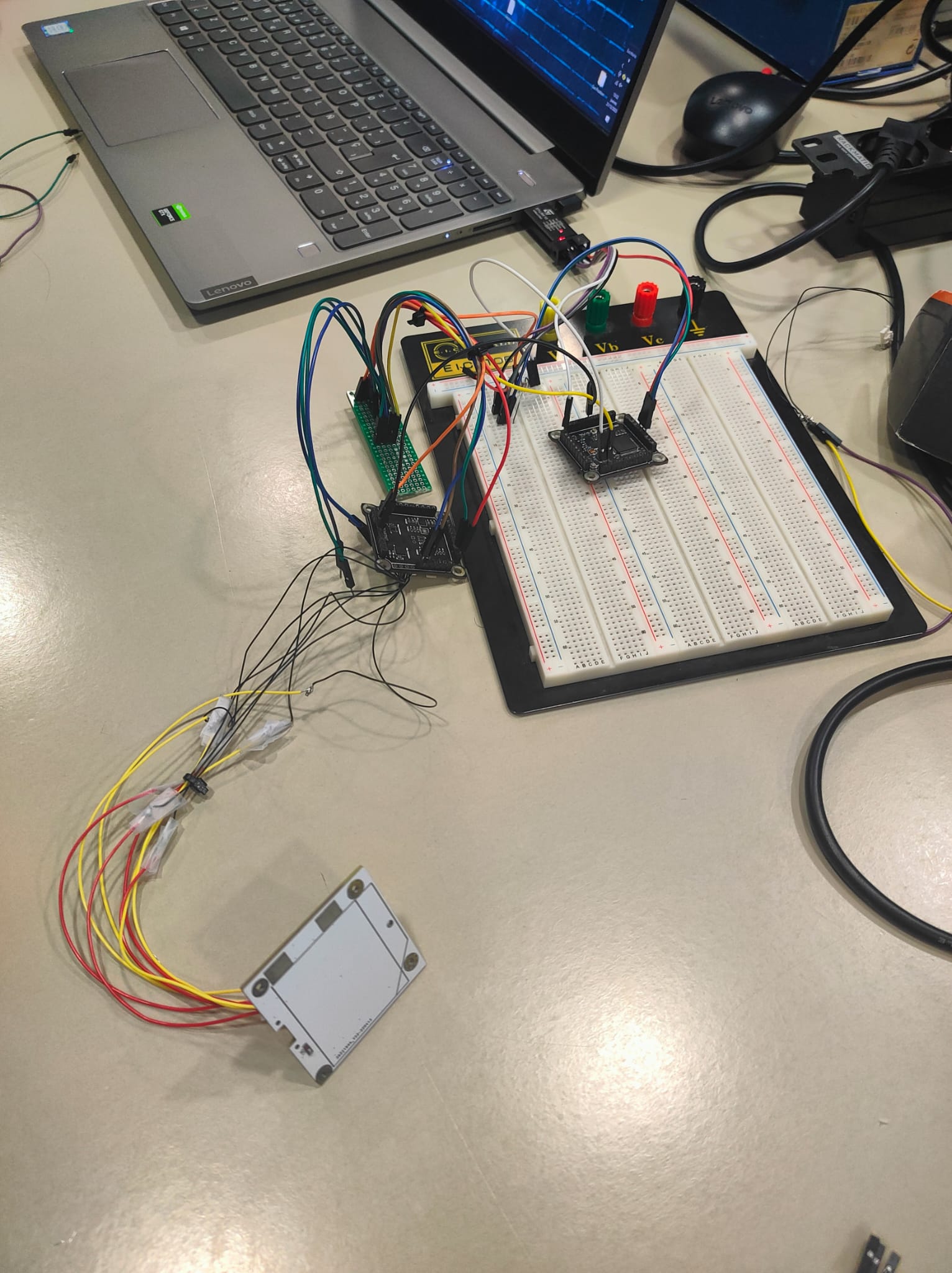
These are the steps to follow:
Step 1: Connect the power supply from the ST-Link/V2 to the ADCS PCB, OBC PCB and lateral board.
Step 2: With the help of the multimeter, check that the VCC inputs pins has the correct value
Step 3: Connect the OBC payload to the computer using SWDIO pins
Step 4: Prepare a code that can read from the photodiode using I2C
Step 5: Connect the OBC to the ADCS PCB using SCL, SDA and ADC-PH pins
Step 6: Connect the lateral board with the ADC-PH pin to the same pins from the 2 PCBs
Step 7: Run the code into the OBC and look in the memory register to see if the communication between the OBC and the ADCS has been done.
This is the code used for the OBC-ADCS photodiode and ADC test:
#include "main.h"

/* Private includes ----------------------------------------------------------*/
/* USER CODE BEGIN Includes */
	int buf[100];
/* USER CODE END Includes */

/* Private typedef -----------------------------------------------------------*/
/* USER CODE BEGIN PTD */

/* USER CODE END PTD */

/* Private define ------------------------------------------------------------*/
/* USER CODE BEGIN PD */

/* USER CODE END PD */

/* Private macro -------------------------------------------------------------*/
/* USER CODE BEGIN PM */

/* USER CODE END PM */

/* Private variables ---------------------------------------------------------*/
ADC_HandleTypeDef hadc1;

I2C_HandleTypeDef hi2c1;

UART_HandleTypeDef huart2;

/* USER CODE BEGIN PV */

/* USER CODE END PV */

/* Private function prototypes -----------------------------------------------*/
void SystemClock_Config(void);
static void MX_GPIO_Init(void);
static void MX_USART2_UART_Init(void);
static void MX_I2C1_Init(void);
static void MX_ADC1_Init(void);
/* USER CODE BEGIN PFP */

/* USER CODE END PFP */

/* Private user code ---------------------------------------------------------*/
/* USER CODE BEGIN 0 */

/* USER CODE END 0 */

/**
  * @brief  The application entry point.
  * @retval int
  */
int main(void)
{
  /* USER CODE BEGIN 1 */

  /* USER CODE END 1 */

  /* MCU Configuration--------------------------------------------------------*/

  /* Reset of all peripherals, Initializes the Flash interface and the Systick. */
  HAL_Init();

  /* USER CODE BEGIN Init */

  /* USER CODE END Init */

  /* Configure the system clock */
  SystemClock_Config();

  /* USER CODE BEGIN SysInit */

  /* USER CODE END SysInit */

  /* Initialize all configured peripherals */
  MX_GPIO_Init();
  MX_USART2_UART_Init();
  MX_I2C1_Init();
  MX_ADC1_Init();
  /* USER CODE BEGIN 2 */
  	int16_t data_ph=0,temperature;
  	float temp=0;
  	//tcn_raw_data data;
  	int i=1;
  	//tcn_scaled_data scaled_data;
  /* USER CODE END 2 */

  /* Infinite loop */
  /* USER CODE BEGIN WHILE */
  while (1)
  {
    /* USER CODE END WHILE */
	  HAL_ADC_Start(&hadc1);
	  	  HAL_ADC_PollForConversion(&hadc1,20);
	  	  data_ph=HAL_ADC_GetValue(&hadc1);
	  	  //TCN_readTemperature(&data);
	  	  //TCN_convertTemperature(data,&scaled_data);
	  	  //temp=(scaled_data.temperature*100);
	  	  //temperature=(int)temp;
	  	  //sprintf((char*)buf,"%d   %d    %d \r\n",data_ph,temperature,i);
	  	  //HAL_UART_Transmit(&huart2, buf, strlen((char*)buf), HAL_MAX_DELAY);
	  	  HAL_Delay(100);
	  	  i++;
    /* USER CODE BEGIN 3 */
  }
  /* USER CODE END 3 */
}After a few usual connection issues, the test went smoothly from what was basically the first attempt. Having a halogen lamp with multiple modules, we could test the reading with a lot of different settings, and we found that the number of modules that are lit is almost proportional to the value we read, meaning the test was in fact a success. Below are the results for 3 different light readings: no lights, 2 lights and 7 lights. The relevant variable is "data_ph", marked in yellow since it has just changed value.

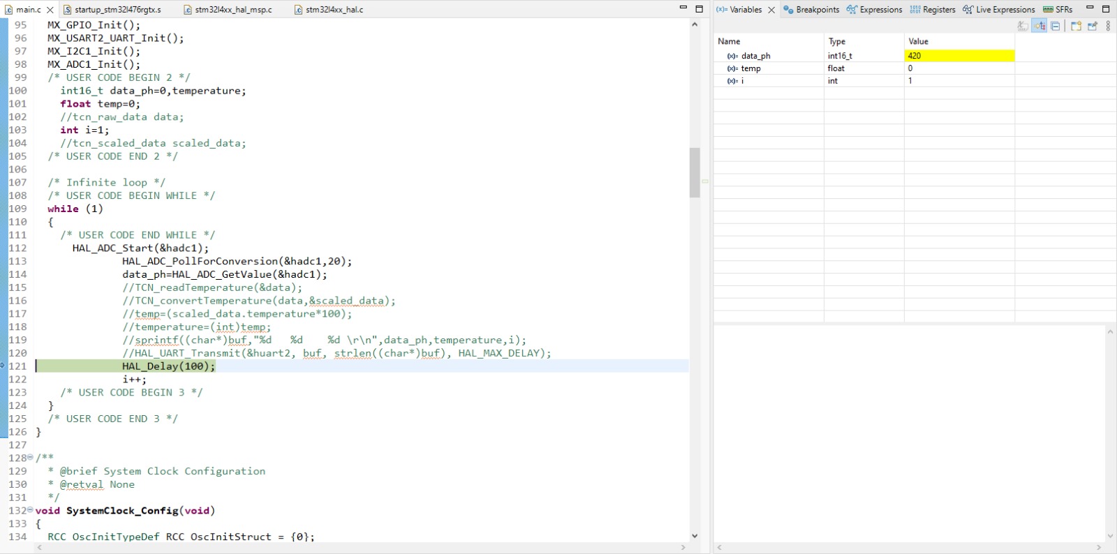
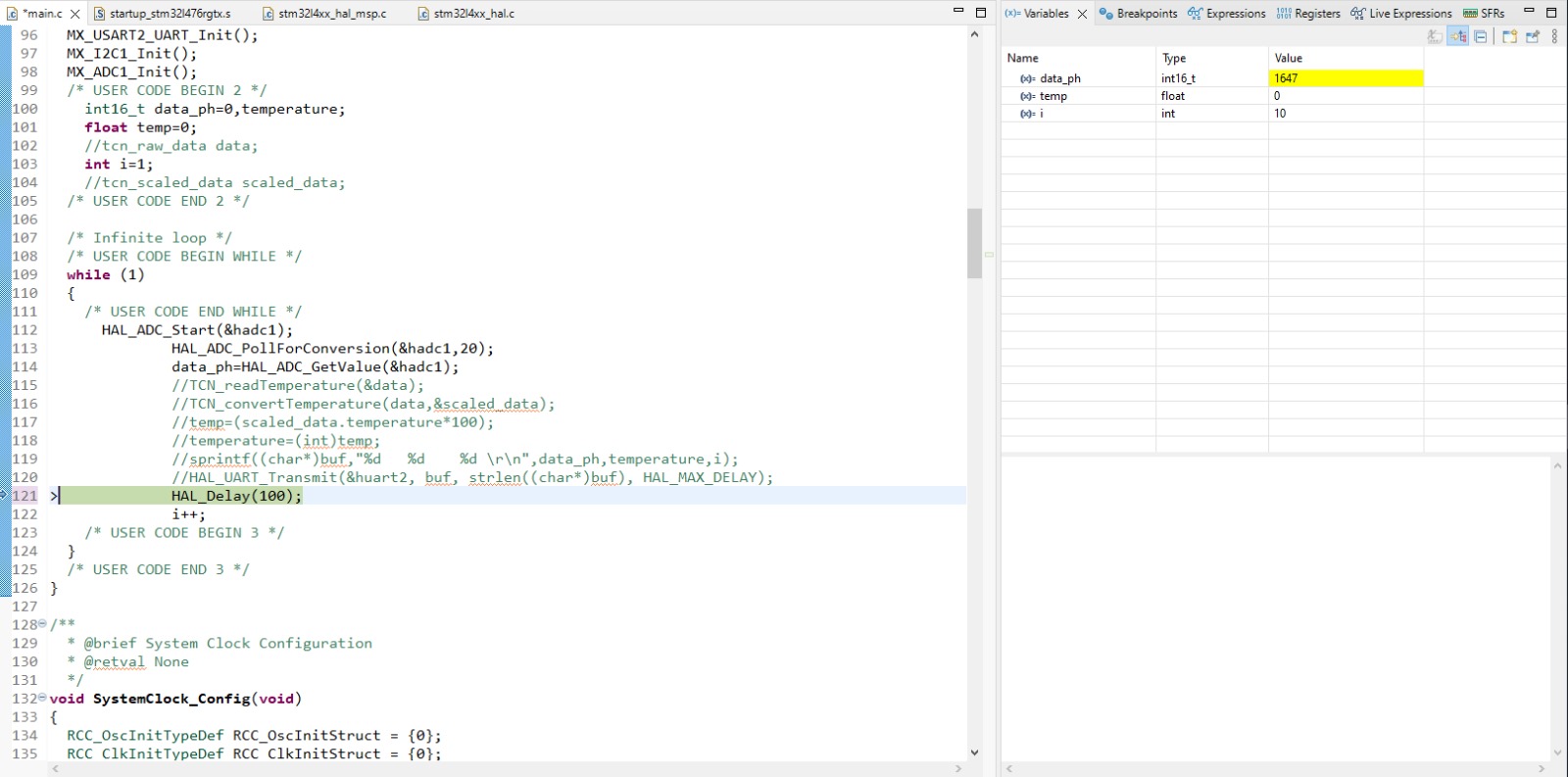
In this test, apart from the usual connection issues, we encountered no notable anomalies.
The ADCS-OBC photodiode data read and ADC data converting test was a complete success, meaning we have managed to test another one of the functionalities of the system and that we are getting closer to a fully integrated system test.
# Electrical Ground Support Equipment (EGSE) # EGSE - Wiring and SetupThe main objective of this section is to document and explain how to proceed with the wiring of the different parts of the EGSE to use it correctly. Additionally, it will explain the fundamentals for operating it properly.
The EGSE does not have all the SSVs interconnected by default, so we will need to create cable buses to interconnect the SSVs, we also need to prepare some special pieces to hold certain parts, such as the solar panels and the bottom board with the kill switches.
Next, we can see an render of the EGSE without connections and without any SSVs. Therefore, we will proceed with documenting the necessary interconnections for the EGSE and the properties it offers

First, we need to prepare the interconnection buses, so we will start by creating these using mainly PicoBlade and PicoClasp connectors (Before making the cables, we will need to ensure they have the correct length)
| ID | From | Num of cables | Connector | To | Num of cables | Connector | Lenght (mm) |
| 1 | Lat +Z | 10 | PicoBlade | PCB Connector | 10 | PicoBlade | |
| 2 | PCB Connector | 10 | PicoBlade | ADCS | 10 | PicoClasp | |
| 3 | Lat -Z | 10 | PicoBlade | PCB Connector | 10 | PicoBlade | |
| 4 | PCB Connector | 10 | PicoBlade | ADCS | 10 | PicoClasp | |
| 5 | Lat +X | 10 | PicoBlade | PCB Connector | 10 | PicoBlade | |
| 6 | PCB Connector | 10 | PicoBlade | ADCS | 10 | PicoClasp | |
| 7 | Lat -X | 10 | PicoBlade | PCB Connector | 10 | PicoBlade | |
| 8 | PCB Connector | 10 | PicoBlade | ADCS | 10 | PicoClasp | |
| 9 | Battery | 2 | PicoBlade | - | - | - | |
| 10 | PCB Connector | 2 | PicoBlade | Bottom Board | 2 | PicoBlade | |
| 11 | Battery Heater & NTC | 3 | PicoClasp | - | - | - | |
| 12 | PCB Connector | 3 | PicoClasp | ADCS | 3 | PicoClasp | |
| 13 | Umbilical | 8 | PicoBlade | PCB Connector | 8 | PicoBlade | |
| 14 | Bottom Board | 15 | PicoBlade | PCB Connector | 15 | PicoBlade | |
| 15 | PCB Connector | 15 | PicoBlade | ADCS | 15 | PicoClasp | |
| 16 | Top Board | 9 | PicoBlade | PCB Connector | 9 | PicoBlade | |
| 17 | PCB Connector | 9 | PicoBlade | ADCS | 9 | PicoClasp |
The +Y magnetometer with the ADCS has to be connected through a simple wire; there is no connector between these parts.
Each cable should be approximately the length specified in the table, which serves as a reference for the cable lengths used in the poCat-LEKTRON EGSE.
In this following diagram, we see the cables we just constructed indicated by black lines. These lines represent which parts of the EGSE will be wired. The colors indicate that they belong to the same part.
If we look closely, all the colored areas are not connected by default; we connect them using the cables we just made

This document specifies the electronic and mechanical aspects necessary to understand and operate the Electronic Ground Support Equipment. Specification and objectives of the EGSE are defined, as well as the board components and power modes available.
The Electrical Ground Support Equipment (EGSE) in a nutshell is a PCB (Printed Circuit Board) to facilitate testing, debugging and maintenance of the PocketQube on the ground. EGSEs in general consist of hardware and/or software elements that perform satellite tests, simulating the missing (sub)system interfaces to ensure full compatibility once integrated into the overall platform.
To achieve it, should allow the placement of all the PCBs contained in the disassembled PocketQube, making all the PCBs accessible and giving access to all the signals of the PocketQube.
| Specifications |
| Allows the placement and connection of the PQ completely disassembled, complying with PQ boards dimension. |
| Allows the placement of the PQ boards on top and bottom view to facilitate the testing. |
| Includes accessible test points for all PQ signals. |
|
Added an external power supply with a protection circuit for overcurrent, overvoltage and reverse polarization. |
|
The external power supply feeds the PQ itself and also charges the battery. For that reason, the EGSE includes the battery charger and EPS regulator of the design, to ensure similarity during the tests. |
| Includes a power management circuit with which, by means of jumpers, the type of supply to be used can be selected. Fig1 |
| Added a connector for programming the MCU, a standard connector such as JTAG. |
| Include lateral boards sliders printed parts to move them away from the EGSE and avoid overheat the EGSE when recharging the cells with a solar lamp. |
| Include bottom board slider printed part to activate and deactivate the kill switches. |
| Add some space and mounting holes for standoffs and the printed 3D parts. |
| Allows vertical positioning of the payload to facilitate antenna deployment, including a vertical connector and a little board adaptor. |
| The project must be carried out in KiCad as it is an open-source tool. |
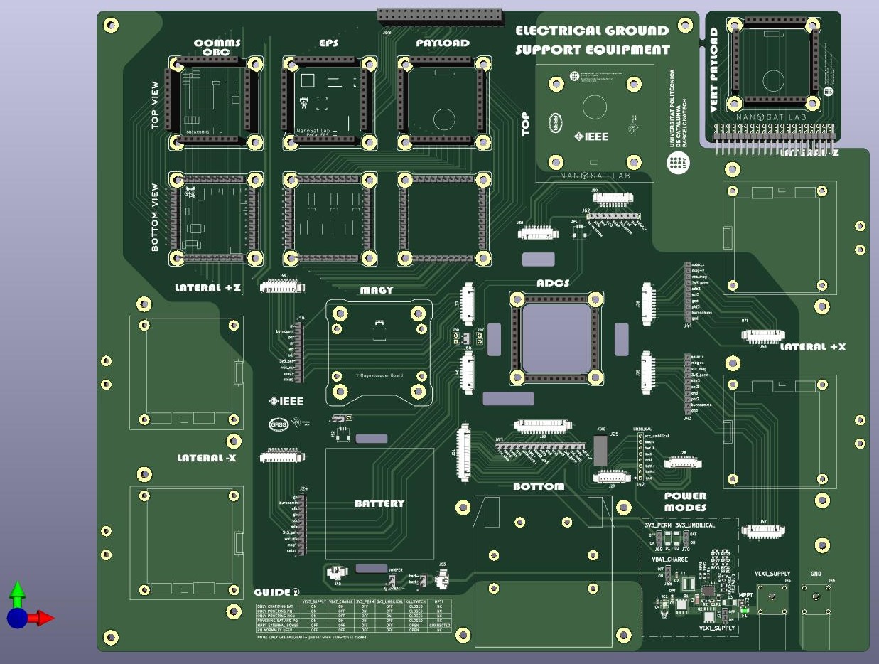 Fig1. EGSE 3D view
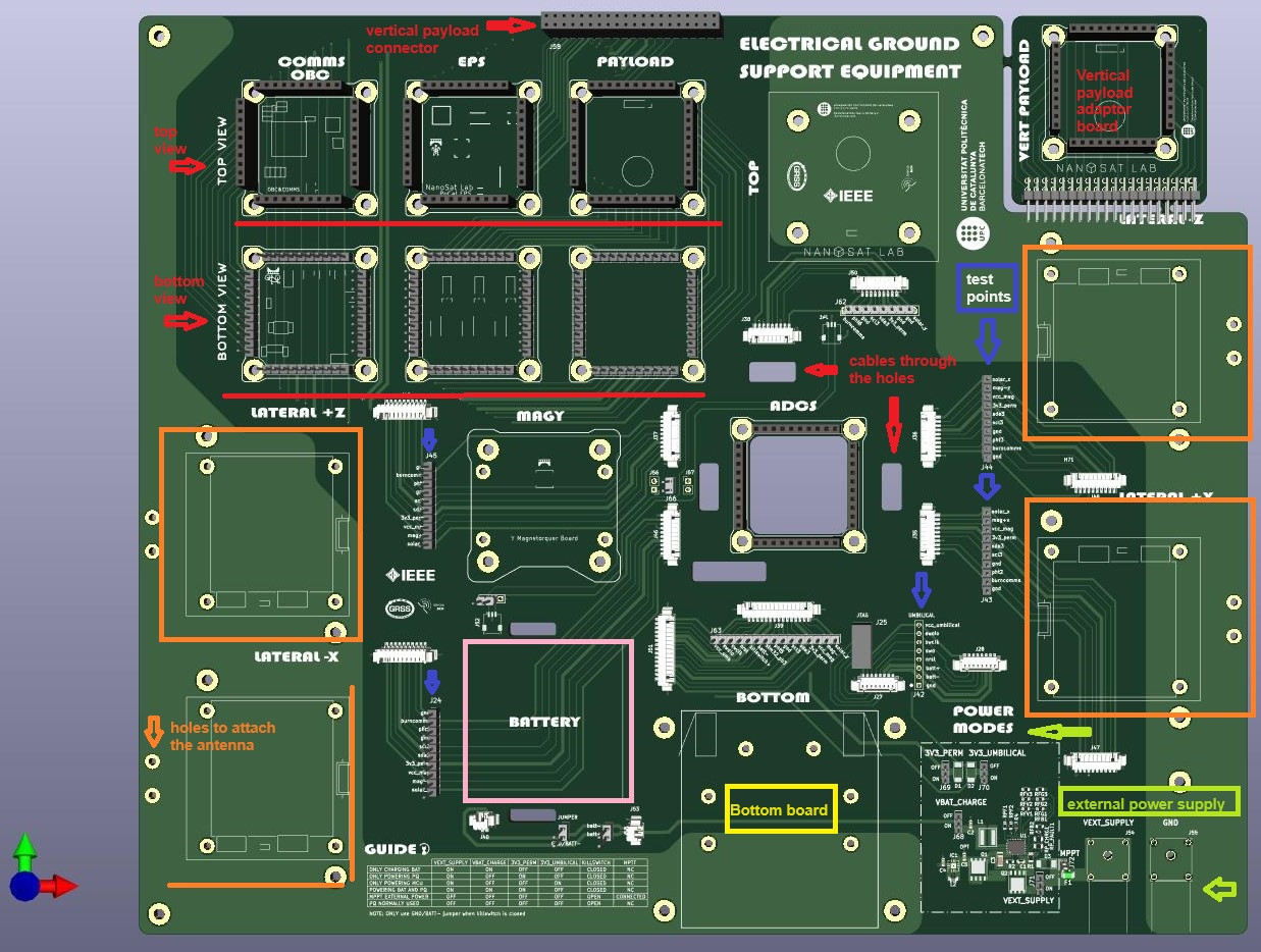
Fig2. EGSE 3D view annotations
Description of the power management options of the EGSE.
The EGSE allows using the PQ with its own battery and solar cells but also permits to use an external power with several configurations. The EGSE interfaces the external power supply with some protections (overcurrent, overvoltage and reverse polarization) and uses the battery charger or backup and the EPS voltage regulator to mirror the power management of the PQ. The available modes are described in Table 1.
| Power Mode | Description |
| ONLY CHARGING BAT | If it's only necessary to charge the battery on the same conditions of the PQ and the power on the PQ it's not needed |
| ONLY POWERING PQ | Use of the PQ with the external power source, but without charging the battery. |
| ONLY POWERING MCU | Mode to program the MCU without charging the battery or using the other subsystems. |
| POWERING BAT AND PQ | Nominal mode of the PQ, but using an external power source. |
| MPPT EXTERNAL POWER | Mode that allows to simulate the power of the solar cells with the external power source. Connect the MPTT EGSE pin to the pin on the EPS board directly with a long cable. |
| PQ NORMALLY USED | Without using an external power source, mode nominal of the PQ using the battery and solar cells, the external power is isolated of the PQ. |
Table 1. Power modes description
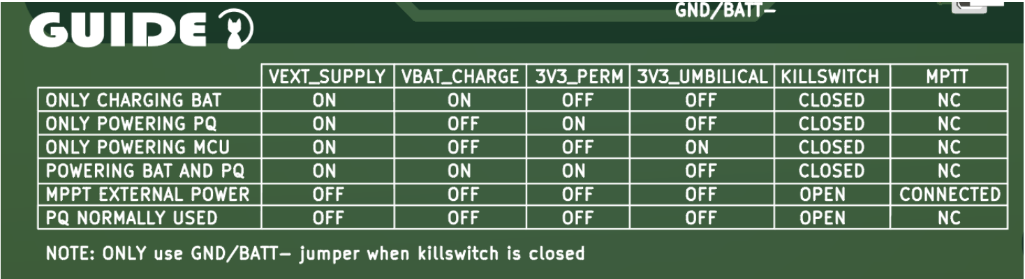
Fig3. Jumper position power modes EGSE

Fig 4. Physical position of the jumpers on the EGSE
# Mechanisms # COMMS Antenna deployer ## Introduction The antenna deployment system is a critical mechanical assembly designed to secure the COMMS antenna in its stowed configuration during launch and ensure a reliable release once in orbit. The mechanism integrates structural, thermal, and elastic components to achieve a fail-safe deployment. 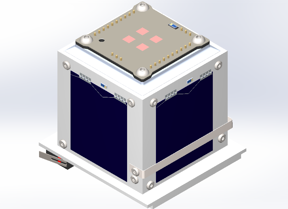 [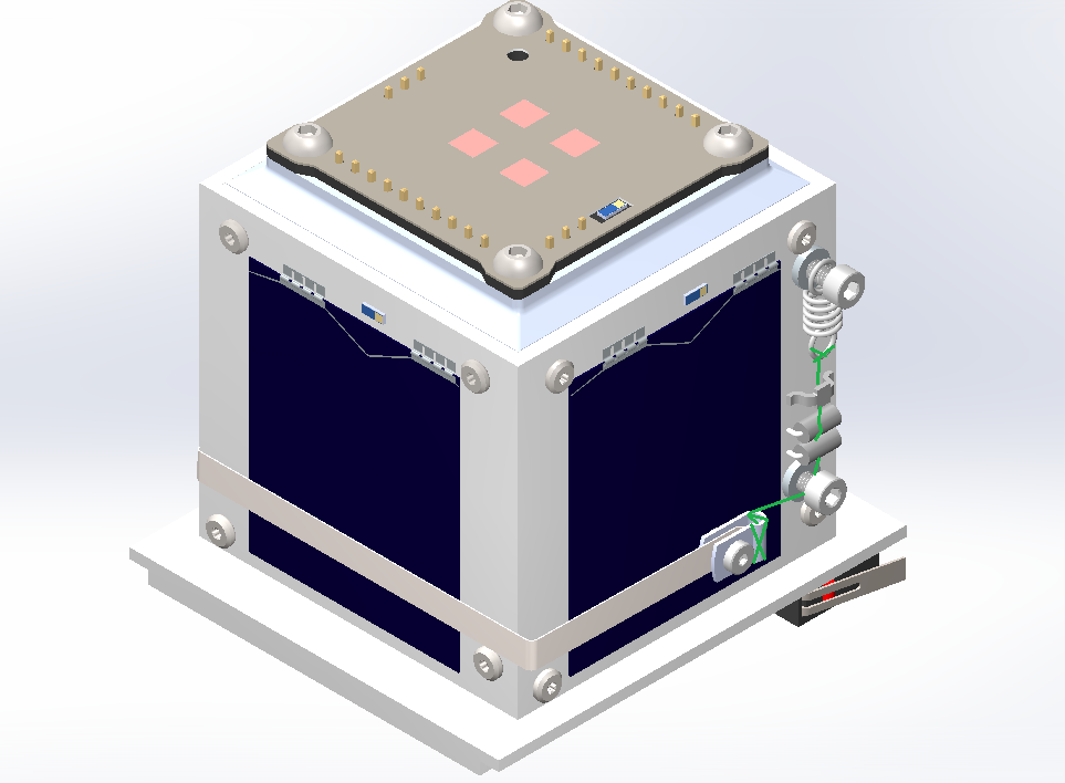](https://wiki.nanosatlab.space/uploads/images/gallery/2026-03/46limage.png) #### 1.1 System Components The assembly consists of the following key elements: - Tether: A high-strength Dyneema string. - Actuators: Two low-impedance resistors (acting as thermal knives) mounted on a dedicated lateral PCB. - Mechanical Routing: An SMT Jumper (Harwin S1731-46R) used as a precision guide and two M2.5 screws secured with thread inserts. - Tensioning System: A high-stiffness extension spring (McMaster-Carr 5108N98) and a cable clip attached to the antenna tip. #### 1.2 Functional Description The Dyneema string wraps around the satellite's perimeter, providing the primary constraint for the antenna. From its attachment point at the cable clip, the tether is routed to a primary screw that acts as a 90º pivot. Following the pivot, the string passes directly over the thermal knives. To ensure high-reliability ignition, the SMT Jumper is positioned to provide constant downward pressure, forcing the Dyneema into direct contact with the resistors. #### 1.3 Launch Integrity To survive the high-vibration environment of the launch vehicle, the system must remain under constant tension. This is achieved by the extension spring, which compensates for any mechanical tolerances and prevents the antenna from oscillating or "wiggling." This tension ensures that the tether remains correctly seated over the thermal knives until the deployment sequence is initiated by heating the resistors to the tether's melting point. ## Description The resistor is currently set at 4.7 Ohms, but further tests—including deployment in vacuum conditions—are planned to confirm its suitability. Other resistor values may offer better performance, so a trade-off analysis is needed to optimize results. The wire connecting the antenna to the thermal knife is a dyneema, specifically commercially used fishing wire made from polyethylene. More precisely, it is ultrahigh-molecular-weight polyethylene (UHMWPE), a material known for its remarkable properties, including extremely high tensile strength (up to 26 kg), making it ideal for high-stress environments, such as rocket launches. In terms of thermal properties, UHMWPE has a breaking temperature between 120°C and 130°C. The antenna is made from metallic metric tape, a coated stainless steel material. One end of the wire will be secured a cable clip at the antenna with a knot, while the other end will be tied to the spring. A final knot design is yet to be selected, as it will need to be validated during the vibration phase of environmental testing. There are two inhibitors preventing the antenna's deployment: 1. Physical Inhibitor: The kill switches on the satellite, which disconnect the PocketQube from the battery while inside the deployer. 2. Software Inhibitor: The INIT mode, which enforces a 45-minute standby period after the kill switches are depressed, as described in the *[Satellite Operation Modes](https://wiki.nanosatlab.space/books/cat-introduction-requirements/page/satellite-operational-modes)* section. ## Mechanical Integrity Calculations The following calculations verify the mechanical integrity of the jumper during the launch phase of the PocketQube. The objective is to ensure that vertical forces acting on the component do not lead to pad failure. ##### [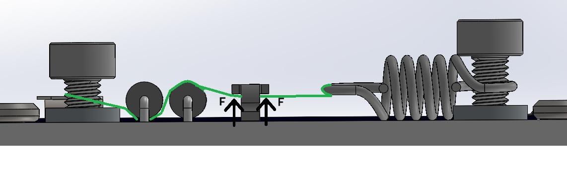](https://wiki.nanosatlab.space/uploads/images/gallery/2026-02/deploymentforces.jpg)Spring Force The axial force exerted by the spring is determined by the formula Fs = k\*x. To establish a worst-case scenario for structural integrity, a total displacement of 3mm is assumed. This value accounts for a 1.5 mm installation pre-tension and an additional 1.5 mm dynamic displacement caused by launch vibrations and antenna mass. Using the McMaster-Carr 5108N98 spring: - **Spring Rate:** 2.758 N/mm - **Total Extension:** 3 mm} - **Resulting Axial Force:** 8.27 N ##### Static Case In the static configuration, the axial force is decomposed into vertical components based on the thread geometry. Due to the "pulley effect" created by the Dyneema thread passing through the jumper, the vertical load is the sum of the components on both sides: [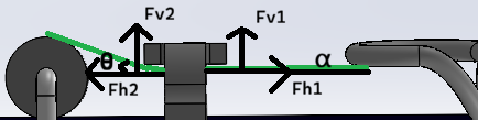](https://wiki.nanosatlab.space/uploads/images/gallery/2026-02/T41image.png) Fv1= F \* sin ⍺ = 0 N Fv2 = F \* sin θ = 2.28 N Fapplied = Fv1+ Fv2 = 2.28 N (Angles computed as ⍺ = 0, θ = 17.75º) At this level the component is well within its safety margin, as each pad is estimated to support up to 4.13 N. ##### Vertical Displacement Case The launch environment introduces random vibrations that induce lateral oscillation in the spring and a displacement that modifies the previous values. [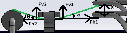](https://wiki.nanosatlab.space/uploads/images/gallery/2026-02/98Pimage.png) To calculate this displacement, we first determine the lateral stiffness (as it's not provided by the manufacturer) and the resonance frequency: 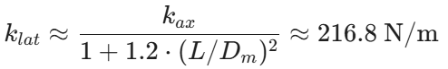 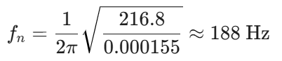 Frequency of 188Hz won't be affected by sinusoidal vibration but can be critical in random vibration. Using ESA's PSD profile (0.16g2/Hz at 188Hz) the following formula is used to obtain effective acceleration, and then, converted into physical distance. 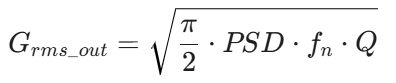 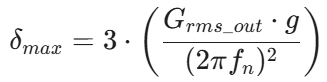 Obtaining 21.7Grms and a displacement of 0.45mm As said, during peak vibration, the dynamic displacement alters the thread angles, increasing the vertical load on the jumper. Fv1= F \* sin ⍺ = 2.7 N Fv2 = F \* sin θ = 2.28 N Fapplied = Fv1+ Fv2 = 4.98 N (Angles computed as ⍺ = 21.21º, θ = 17.75º) The total vertical force of 4.98N is distributed across two solder pads. While the load per pad exceeds the static ideal, it remains within a manageable range for the Harwin S1731-46R. # KillswitchesThe satellite has 2 killswitches located on the bottom PCB. These are connected in series, allowing for redundancy in case one of them fails.
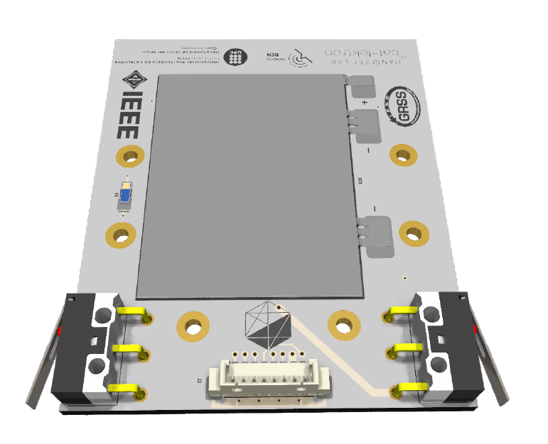
Figure 1: Killswitches in Bottom PCB
During operations where the satellite needs to be disconnected, the switches should be pressed. When the satellite is inside the deployer rail, the switches will be pressed, keeping the satellite off. Once in space, the deployer rail will release the switches, turning the satellite on by releasing the killswitches. The location of the killswitches follows the PocketQube standard [PQ Standard Alba] recommendation, positioned on the bottom PCB, just below the direct contact area with the deployer rail.
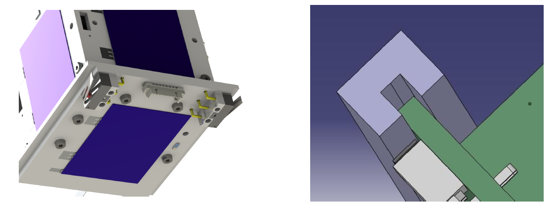
Figure 2 and 3: Killswitches Close Look and PQ Standard Killswitch location
If we analyze the general electrical scheme of the satellite in figure 4, we can see that both killswitches interfere in the direct battery line. This allows that while both are pressed, the battery will not connect to the satellite, keeping it turned off. However, the solar cells will remain connected to the EPS, and with a sun simulator or sunlight, even under AM1.5 (air mass coefficient defines the direct optical path length through the Earth's atmosphere) conditions, the satellite could be started. Therefore, it is necessary to prevent sunlight from reaching the solar cells while the killswitches are pressed.
If we analyze the general electrical scheme of the satellite in figure 3.66, we can see that both killswitches interfere in the direct battery line. This allows that while both are pressed, the battery will not connect to the satellite, keeping it turned off. However, the solar cells will remain connected to the EPS, and with a sun simulator or sunlight, even under AM1.5 conditions, the satellite could be started. Therefore, it is necessary to prevent sunlight from reaching the solar cells while the killswitches are pressed. This is a current design flaw that is under revision and awaiting further updates after design changes.
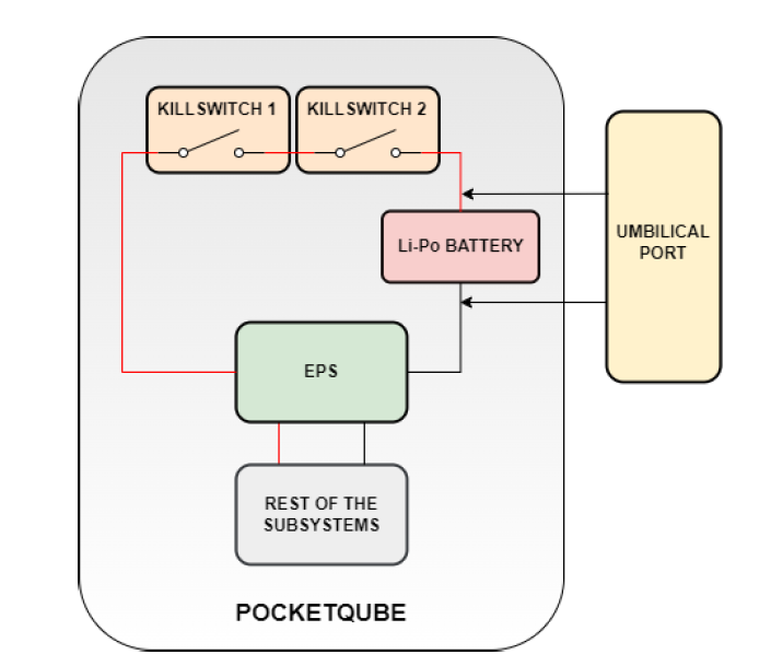
Figure 4: General Electric Scheme of the satellite with the killswitches and umbilical port
It can be observed that, even though the kill switches are pressed, the satellite still has a direct connection to the umbilical port, allowing communication with the satellite as well as the ability to charge the battery through the umbilical port.
Once the satellite is placed in the deployer rail and the kill switches are engaged, the battery will remain in standby mode, meaning it won’t charge or discharge actively. However, this will lead to a slow, passive discharge of the battery over time.
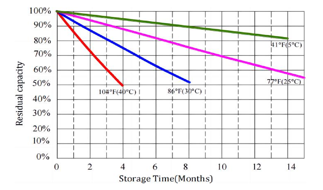
Figure 5: Capacity Discharged vs Storage Time and Temperature
According to the manufacturer’s data (figure 5), the rate of discharge depends on the temperature and how long the battery remains without the ability to charge. While these values are theoretical, in practice, the actual discharge rate can vary due to several factors. Nonetheless, these estimates provide a general idea of how long the satellite’s battery can remain without charging.


