On-Board Computer & Software (OBC/OBSW)
Subsystem Description
Functional Architecture
Conceptually, the On-board Computer (OBC) acts as the brain governing the spacecraft, serving as the central component within the overall architecture of this system. It plays a pivotal role in a complex system that accommodates the following five distinct sub-modules: Electrical Power Supply (EPS), Communication System (COMMS), Attitude Determination and Control System (ADCS), and the payload (P/L).
In other words, the main purpose of the subsystem is to perform the housekeeping of the overall satellite. In this regard, performing both data processing and storage in a timely manner while maintaining a low power consumption is crucial so as to guarantee an efficient and robust performance of the PocketQube. In light of this, the Flight Software (FSW) running on the OBC needs then to be carefully designed by the application writter in order to meet the time requirements linked to the varied tasks that the satellite is expected to perform. A common technique used in embedded systems in order to fix this time constraint is implementing Real-Time Operating Systems (RTOS). In the PoCat project, FreeRTOS has been the open-source RTOS selected to manage the on-board FSW.
On the other hand, the OBC hardware needs to accommodate the FSW by providing enough resources for a correct execution. In summary, the breakdown of the OBC from the hardware perspective consists of a low-power but high-performance ARM Cortex M4 microprocessor, volatile and non-volatile memory banks for data storage, interfaces that reach out to peripherals and data buses interconnecting the whole system architecture.
To ensure the desired behaviour of the PocketQube, it is necessary for both software and hardware to converge seamlessly. This will enable the OBC to efficiently manage various tasks that play a critical role in determining the behavior of the picosatellite. In summary, the tasks that are performed by the On-Board Computer for the PoCat space mission are listed below:
- Task scheduling.
- Inter-task communication.
- Power management.
- Telecommand processing.
- Telemetry data handling.
- Payload data acquisition.
- Attitude determination and control.
- Error handling.
Requirements
| Subsystem | ID | Requirement |
|---|---|---|
| OBC | OBC-0010 | The OBC shall monitor all spacecraft subsystems. |
| OBC | OBC-0020 | The OBC shall have a Scheduler which determines the execution of different tasks through time. |
| OBC | OBC-0030 | The OBC shall provide and store the following housekeeping data: Satellite mode, Boot count, OBC error events, Internal satellite communication error events, RAM memory usage. |
| OBC | OBC-0040 | The OBC shall retrieve and store housekeeping data for all spacecraft subsystems. |
| OBC | OBC-0050 | The OBC shall monitor all satellite subsystems in order to verify their nominal behavior. |
| OBC | OBC-0060 | The OBC shall execute TC received from the GSeg. |
| OBC | OBC-0070 | The OBC shall be able to control and command all subsystems via its interfaces. |
| OBC | OBC-0080 | The OBC shall retrieve and store scientific data from the Payload. |
| OBC | OBC-0090 | The OBC shall have data interfaces with all subsystems. |
| OBC | OBC-0100 | The OBC power supply voltage shall be 3.3 V. |
| OBC | OBC-0110 | The OBC shall enable the manual transition between satellite modes if a TC from the ground is received. |
| OBC | OBC-0120 | The OBC shall automatically transition between satellite modes based on battery levels. |
| OBC | OBC-0130 | The OBC should allow in-orbit changes of its configuration. |
| OBC | OBC-0140 | The OBC shall implement a command-less timer that triggers a recovery routine if a telecommand from the GS is not received after a certain period. |
| OBC | OBC-0150 | The spacecraft shall allow modifications to the OBC Software after the satellite assembly is complete and while on ground. |
| OBC | OBC-0160 | The spacecraft shall have a timer, set to a minimum of 30 minutes, before operations or deployment of the antennas. |
| OBC | OBC-0170 | No radio emission shall be allowed after the spacecraft has been integrated within the PocketQube deployer until 45 minutes after deployment. |
Hardware Design
Design Choices
Up next is provided a table including the most important information of the OBC. In the following sections is found information about each one of them as well as the overall design of the system.
Quick Facts Table
| Component | Value |
|---|---|
| Microcontroller | STM32L476RG |
| Core | ARM Cortex-M4 |
| Generation | STM32L4 Series of ultra-low-power MCUs |
| Flash Memory | 1 MB |
| SRAM | 128 KB |
Table 1: OBC Hardware Quick Facts Table
Microcontroller Unit (MCU)
The selected microcontroller unit is the STM32L476RG. Among its main features one can find outstanding processing performance, fast interrupt handling, low gate count and ultra-low-power consumption. Some of the reasons that back up this choice are provided next:
- Common industry use, therefore there is a lot of documentation about it on STMicroelectronics' website, but also a significant amount of online tutorials which showcase how this device could be used for a multitude of tasks.
- Size of the flash memory and effiency of SRAM, paired up with the 32 KB of hardware parity check, enabling the creation a buffer for important data to be safely stored in.
- The availability of a wide array of peripheral communications including I2C, USART, SPI, and SWPM create a very flexible environment for trying out several methods of setup and communication. This is also relevant considering the modular approach to the
- The number of internal and possible external clocks with a capacity of oscillating to 80 MHz allows the satellite to operate under multiple different modes, each with different clock settings well-suited to power management applications.
The microcontroller hosts an overall 4 GByte memory area, at adresses ranging between 0x0000 0000 and 0xFFFF FFFF. Accessible for our use are two SRAM memories providing a total sum of 128KB and a Flash memory with an storage capacity of 1MB.
| Memory | Addresses | Storage Capacity | Boot Area | Application Code |
|---|---|---|---|---|
| SRAM1 | 0x2000 0000 - 0x2003 FFFF | 96 KBytes | NO | NO |
| SRAM2 | 0x1000 0000 - 0x1000 7FFF | 32 KBytes | NO | NO |
| Flash | 0x0800 0000 - 0x080F FFFF | 1 MByte | YES | YES |
Table 2: Embedded Memories information
The flash memory is also divided in two 512KBytes banks, enabling read-while-write operations. The embedded SRAM can be accessed in read/write at CPU clock speed with 0 wait states.
Clocks
The MCU is provided with internal clocks but a pair of external clocks are accommodated for clock configuration. This is due to the fact that the speed of the MCU will be slown down depending on the state of the battery as well as due to the necessity of high speeds by the K-Band payload.
These two external clocks will provide redundancy and a stable reference signal to the OBC ensuring proper timings. One of this clocks is a 32.768KHz SMD Low Profile Crystal (ABS09-32.768KHZ-7-T), providing a lower speed signal while the other clock, a ECX-32 SMD CRYSTAL(ECS-120-18-33-JEM-TR3), provides a high speed signal at a frequency 32 MHz. Both were selected due to their temperature operative ranges as well as package size, while also considering availability.
PoL Controls
While the PoL Controls do not belong to the OBC subsystem in on of itself they are located in the OBC-COMMS board and controlled by the MCU. These are requiered to easily shutdown parts of the system as well as ensuring voltages in critical points. Even though this task could moreless be performed by transistors, the use of PoL IC improves reliability and offers a safer alternative.
The selected IC for this task is the BD2232G-GTR due to it being equipped with the functions of over-current detection, thermal shutdown and under-voltage lockout. The package size and thermal properties also match the system requirements.
Schematic Design
MCU
The MCU is undoubtedly the most complex piece of the OBC-COMMS PCB in terms of connectivity. It communicates with the rest of the system using DACs, ADCs, UART, I2C (to a great extent), SPI and GPIOs. The schematic of the MCU is provided next:

Figure 1: MCU Schematic
In order to avoid high frequency interferance with the voltage supply of the MCU seven capacitors are placed in parallel before the input resulting in the following configuration.
Figure 2: MCU Decoupling Capacitors Schematic
Now a table with some information about each one of the PINs of thee MCU is given and most relevant explanations are provided later:
| Pin Number / Name | PCB Pin Name | Type | Description |
|---|---|---|---|
| 1/VBAT | VCC | Power | General Power line at 3.3V |
| 2/PC13 | NC | - | - |
| 3/PC14 | OSC32_IN | Input | 32 kHz Oscillator Input |
| 4/PC15 | OSC32_OUT | Output | 32 kHz Oscillator Output |
| 5/PHO | OSC_IN | Input | 12 MHz Oscillator Input |
| 6/PH1 | OSC_OUT | Output | 12 MHz Oscillator Output |
| 7/NRST | NRST | Digital Input | STM32 Reset Pin |
| 8/PC0 | SCL3 | I2C | I2C3 Clock Bus |
| 9/PC1 | SDA3 | I2C | I2C3 Data Bus |
| 10/PC2 | SEL_PH0 | Digital Output | Selector for Photodiode Multiplexer |
| 11/PC3 | NC | - | - |
| 12/VSSA | GND | Power | Ground |
| 13/VDDA | VCC | Power | General Power line at 3.3V |
| 14/PA0 | BATT_NTC | Analog Input | Battery Temperature NTC Sensor |
| 15/PA1 | ADC_PL | Analog Input | ADC Input |
| 16/PA2 | X | NC | Unused Pin for Future or No Use |
| 1/PA3 | CHRGOFF | Digital Output | Battery Charging Enable Pin |
| 18/VSS | GND | Power | Ground |
| 19/VDD | VCC | Power | General Power line at 3.3v |
| 20/PA4 | CLPROG | Analog Outpot | Charge Current Programming Output |
| 21/PA5 | DAC_PL | Analog Output | DAC Output for Payload |
| 22/PA6 | X | Not connected | Unused Pin for Future or No Use |
| 23/PA7 | PoL_ADCS_POWER_EN | Digital Output | Point of Load Control for ADCS |
| 24/PC4 | FAULT | Digital Input | Battery Charging Fault Status Pin |
| 25/PC5 | ADC_PH | Analog Input | Photodiode Array Output |
| 26/PB0 | STM32_PB0 | GPIO | Connected to STM32 PB0, User Defined |
| 27/PB1 | X | Not connected | Unused Pin for Future Use |
| 28/PB2 | CHRG | Digital Input | Battery Charging Monitoring Pin |
| 29/PB10 | HEATER_EN | Digital Output | Heater Enable Pin |
| 30/PB11 | PoL_BURN_EN | Digital Output | Point of Load Control for Antenna Deployment |
| 31/VSS | GND | Power | Ground |
| 32/VDD | VCC | Power | General Power line at 3.3V |
| 33/PB12 | SX1262_NSS | SPI Chip Select | SX1262 Chip Select |
| 34/PB13 | SCK | SPI Clock | SX1262 SPI Clock |
| 35/PB14 | MISO | SPI MISO | SX1262 SPI Master-In Slave-Out |
| 36/PB15 | MOSI | SPI MOSI | SX1262 SPI Master-Out Slave-In |
| 37/PC6 | PoL_P/L_EN | Digital Output | Point of Load Control for Payload |
| 38/PC7 | X | Not connected | Unused Pin for Future or No Use |
| 39/PC8 | X | Not connected | Unused Pin for Future or No Use |
| 40/PC9 | SX1262_NRST | Digital Input | SX1262 Reset |
| 41/PA8 | SX1262_BUSY | Digital Ouput | SX1262 Busy Indicator |
| 42/PA9 | STM32_PA9 | GPIO | Connected to STM32 PA9, User Defined |
| 43/PA10 | DIO1 | Digital Iinput | SX1262 Interrupts |
| 44/PA11 | SEL_PH1 | Digital Output | Selector for Photodiode Multiplexer |
| 45/PA12 | SEL_PH2 | Digital Output | Selector for Photodiode Multiplexer |
| 46/PA13 | SWDIO | Serial Wire I/O | STM32 Debug Port |
| 47/VSS | GND | Power | Ground |
| 48/VDDUSB | VCC | Power | General Power line at 3.3V |
| 49/PA14 | SWCLK | Serial Wire | STM32 Debug Port |
| 50 /PA15 | STM32_PA15 | GPIO | Connected to STM32 PA15, User Defined |
| 51/PC10 | UART_TX | UART (Output) | UART TX Bus to P/L |
| 52/PC11 | UART_RX | UART (Input) | UART RX Bus to P/L |
| 53/PC12 | X | Not connected | Unused Pin for Future or No Use |
| 54/PD2 | X | Not connected | Unused Pin for Future or No Use |
| 55/PB3 | SWO | Serial Wire | STM32 Debug Pin |
| 56/PB4 | X | Not connected | Unused Pin for Future or No Use |
| 57/PB5 | PFO | Power | Power Fault Output |
| 58/PB6 | SCL1 | I2C | I2C1 Clock Bus |
| 59/PB7 | SDA1 | I2C | I2C1 Data Bus |
| 60/BOOT0 | Boot0 | Boot | Boot Pin |
| 61/PB8 | X | Not connected | Unused Pin for Future or No Use |
| 62/PB9 | X | Not connected | Unused Pin for Future or No Use |
| 63/VSS | GND | Power | Ground |
| 64/VDD | VCC | Power | General Power line at 3.3V |
Table 3: MCU PINs
PoL Control
The Point-of-Load (PoL) control provides powering of critical components of the system, those being the P/L, ADCS, Thermal Knife and the Battery Heater. The IC is powered by the 3.3V line and the schematic follows the manufacturers reference design, with EN/EN# pin being controlled by the OBC with GPIOs (as MCU Outputs).
Figure 3: PoL Controls Schematic
The outputs of these PoL is connected to the vertical connectors on the sides of the PCB.
External Clocks
The OBC external clocks are provided with decoupling capacitors to minimize any noise that might affect the reference signals. The schematics are provided next:
Figure 3: External Clocks Schematic
Capacitors are placed at the extremes of the clocks to reduce the gain of higher harmonics produced by the crystals themselves.
Overall Schematic
A schematic of the whole system is provided now, highlihting the parts with different colours:

Figure 4: Overall OBC Schematic
- Red: The MCU itself, coupled with the pull-up resistors and capacitors it needs for its pins.
- Green: The 4 power switch ICs which can switch several pin outputs to zero (more specifically: P/L_POWER, ADCS_POWER, BURNCOMMS, and HEATER_PWR).
- Light blue: The outside lateral connectors used for system power and data connectivity.
- Dark blue: The Umbilical Power Diode used to protect the circuit from reflections while being directly powered .
- Pink: The 2 external oscillators (Low speed and High speed) used as redundant clocks for the OBC circuit.
- Orange: The MCU's decoupling capacitors used to reduce and filter out noise caused by sudden changes in power demand from a device or component.
- Yellow: The mounting holes for the PCB, which will be used to fixate all the PCB in place with a long screw and give them a common GND pin.
PCB Design
Next an explanation of the OBC side of the OBC-COMMS PCB is given. Information related to the COMMS side is in its respective section. A render of the PCB is provided in the next figure:
Figure 5: OBC-COMMS PCB with OBC Components highlighted
- Light red: MCU.
- Green: Pull-up resistors for I2C.
- Pink: Decoupling capacitors.
- Dark blue: Power switch ICs (PoL Control) and their respective input capacitor.
- Purple: Crystal oscillators and their respective coupling capacitors.
- Crimson red: Umbilical diode and connector.
- Light blue: Input capacitor and resistor for NRST and Boot0 respectively.
The MCU is located at the top layer of the PCB, placed at the left side of the board to keeking most power distribution as far away as possible from the COMMS side of the PCB to minimize interference. This distribution also keeps the I2C pins close to the vertical connectors which helps reduce noise from the PCB. The Decoupling capactitors are placed throughout the board on the STM32 voltage pins.
The I2C Pull-up resistors are simply placed as close as possible to the corresponding pins. This decision also happens to minimize the lenght of the lines as the PINs are close to the vertical conectors. This same philosophy applies to the input capacitor and resistor for NRST and Boot0.
All this components are besides the NRST capacitor are on the top layer. On the bottom layer we find the Power switch ICs (PoL Control) which are once again located as close as possible to the vertical connectors where their outputs match in order to minime power losses, keep lines short and avoid interferences with COMMS. On the same side are the Crystal oscillators which are located at the top right corner as the MCU is then located straight on top of them. This is fundamental as the harmonics generated by these clocks are dangerous to the COMMS subsystem, so keeping them as far as possible from the RF lines and transciever minimizes risk of coupling.
The last piece of the OBC PCB are the Umbilical diode and connector, also on the bottom layer and, once again, close to the vertical connectors for the same reasons as before.
A list of the components as well as some information for each part is provided next:
Microcontroller Unit (MCU)
The table containing the MCU information:
| Characteristic | Description |
|---|---|
| Microcontroller | STM32L476RGT7 |
| MCU Manufacturer | ST |
| Core | ARM Cortex M4 |
| Word Length | 32-bit |
| Frequency (MHz) | 80 |
| Architecture | RISC |
| FPU | Yes |
| Consumption | 9.6mA |
| Interfaces | x3 I2C, x3 SPI, x2 UART, x3 USART, x8 GPIO |
| ADC | 3 |
| DAC | 2 |
| Flash | 1MB |
| RAM | 128KB |
Table 4: MCU Information
Decoupling capacitors
Capacitor C31 is a 4.7uF ceramic capacitor (GRT188R61E475KE13D) with the following characteristics:
| Temp. coeff. or Cap. Change | Temp. Range | Ref. Temp. | Rated Voltage | Capacitance | Capacitance Tolerance | Operating Temp. Range | Mounting Method |
|---|---|---|---|---|---|---|---|
| -15 to 15 % | -55 to 125°C | 25°C | DC 100V | 4.7uF | +/-10% | -55 to 85°C | Flow, Reflow |
Table 5: GRT188R61E475KE13D (C31) Relevant Values
Capacitors C32 to C36 are all 100nF ceramic capacitors (GRM188R72A104KA35J) with the following characteristics:
| Temp. coeff. or Cap. Change | Temp. Range | Ref. Temp. | Rated Voltage | Capacitance | Capacitance Tolerance | Operating Temp. Range | Mounting Method |
|---|---|---|---|---|---|---|---|
| -15 to 15 % | -55 to 125°C | 25°C | DC 100V | 0.1uF | +/-10% | -55 to 125°C | Flow, Reflow |
Table 6: GRM188R72A104KA35J (C32, C33, C34, C35, C36) Relevant Values
Capacitor C37 is a 1uF ceramic capacitor (GRM188R61A105KA61D) with the following characteristics:
| Temp. coeff. or Cap. Change | Temp. Range | Ref. Temp. | Rated Voltage | Capacitance | Capacitance Tolerance | Operating Temp. Range | Mounting Method |
|---|---|---|---|---|---|---|---|
| -15 to 15 % | -55 to 85°C | 25°C | DC 10V | 1uF | +/-10% | -55 to 85°C | Flow, Reflow |
Table 7: GRM188R61A105KA61D (C37) Relevant Values
I2C Pull-up resistors
The I2C PU Resistors (R1, R2, R7, R8) are all 4.7k thick film resistors (CRCW06034K70JNEAC):
| Resistance | Power Rating | Tolerance | Temp. Coefficient | Min. Operating Temp. | Max. Operating Temp. | Voltage Rating |
|---|---|---|---|---|---|---|
| 4.7 kOhms | 100 mW (1/10 W) | 5% | 200 PPM / °C | -55 °C | +155 °C | 75 V |
Table 8: I2C PU Resistors Values (R1, R2, R7, R8)
Crystal Oscillators
The Crystal oscillators present the following capacitors to filter harmonics:
| RefDes | Package | Value | Qty | Description | Manufacturer Code |
|---|---|---|---|---|---|
| C38, C39 | 0402 | 10pF | 1 | Multilayer ceramic capacitors C0G ±2%, 50V | 06035A100GAT2A |
| C40, C41 | 0402 | 3.3pF | 1 | Multilayer Ceramic Capacitors C0G ±5%, 100V | GCM1885C2A200JA16D |
Table 9: Crystal Oscillators Capacitors Values
Umbilical diode (RBS1LAM40ATR)
The umbilical connector boasts two diodes, which are the same component:
| Type | Configuration | Technology | If | Vrrm | Vf | Ifsm | Ir | Vr | Max Op. Temp. |
|---|---|---|---|---|---|---|---|---|---|
| Schottky Diodes | Single | Si | 1 A | 40 V | 340 mV | 40 A | 150 µA | 20 V | +125 °C |
Table 10: Umbilical Diodes Values
Input C&R for NRST and Boot0
NRST and Boot0 make use of the following components:
- The resistor R6 (CRCW040210K0FKEDC):
| Resistance | Power Rating | Tolerance | Temp. Coefficient | Min. Operating Temp. | Max. Operating Temp. | Voltage Rating |
|---|---|---|---|---|---|---|
| 10 kOhms | 63 mW (1/16 W) | 1% | 100 PPM / °C | -55 °C | +155 °C | 50 V |
Table 11: R6 Values
- The capacitor C42 (GRM188R72A104KA35J) is the same as the capacitors C32 to C36 decoupling capaciitors .
Power switch ICs Capacitors
The power switch capacitors are the same as the C37 decoupling capacitor .
PCB Layers
The OBC-COMMS layers are explained on the COMMS section of hardware-
State of the art
The Due to the novel nature of the satellite, research in this area is somewhat restricted. Most of the currently deployed spacecraft are primarily the outcome of educational initiatives and an emerging market. Considering all this, the assessment is focused on three enterprises currently offering market solutions, the already introduced Alba Orbital and FOSSA Systems, along with Citadel Space Systems. It is worth mentioning that the products of the latter company, still do not have experience in space. The 3 reference PocketQubes are Unicorn-2, FOSSASat-2 and Scquire, developed by Alba Orbital, FOSSA Systems and, Citadel Space Systems respectively.
The analysis breakdown of their microcontrollers on-board is performed in table 2.1. The underlying purpose of this comparison is to identify the technology that best meets the requirements of our On-Board Computer. In this regard, the research is focused on the relevant features of the microcontroller selected to fly towards space, such as word length, maximum frequency, architecture among others.
| Organization | Alba Orbital | FOSSA Systems | Citadel Space Systems |
|---|---|---|---|
| PocketQube | Unicorn-2 | FOSSASat-2 | Squire |
| Microcontroller | MSP430 | STM32L4 | TMS570 |
| MCU Manufacturer | TI | ST | TI |
| Core | CPU | ARM Cortex M4 | ARM Cortex R5F |
| Word Length | 16-bit | 32-bit | 32-bit |
| Frequency (MHz) | 16 | 80 | 300 |
| Architecture | RISC | RISC | RISC |
| FPU | No | Yes | Yes |
| Consumption | 6.72mA | 9.6mA | 990mA |
| Interfaces | x1 I2C, x1 SPI, x1 UART | x3 I2C, x3 SPI, x2 UART, x3 USART, x8 GPIO | x2 I2C, x5 SPI, x4 UART, x16 GPIO |
| ADC | 8 | 3 | 2 |
| DAC | - | 2 | - |
| Flash | 16KB | 1MB | 4MB |
| RAM | 512B | 128KB | 512KB |
Table x: State of the art comparison
According to the previous table, the microcontroller selected by the emergent picosatellite companies are Texas Instruments (TI) and STMicroelectronics (ST). Regarding the processor core, it is common for the microcontrollers to be based upon a processor manufactured by another enterprise. In this case, the STM32L4 and the TMS570 are based on ARM Cortex M4 and ARM Cortex R5F respectively, both developed by Arm. However, TI has opted to develop the Central Processing Unit (CPU) core themselves. Furthermore, the critical features that significantly impact microcontroller per-On-board computer software development for PocketQubes formance are frequency and word length.
On the one hand, the frequency establishes the speed of the CPU, expressed in Hertz or MegaHertz represents the number of clock cycles per second. In our scenario, the TMS570 is the fastest in terms of intruction execution with 300 MHz, followed by the STM32L4 with 80 MHz and finally, the slowest being MSP430 at 16 MHz. On the other hand, the word length determines the width of the processor registers and the bus data width. Consequently, the memory space, data and instruction handling, and data precision are dependent on this parameter. For this reason, the processing performance of the 32-bit microcontroller from FOSSA Systems and Citadel Space Systems is more powerful, than the 16-bit selected by Alba Orbital.
However, performance comes together with power consumption so adjusting the system functioning to its requirements is key. In this context, the assessment should focus on the optimum trade-off between performance and power consumption where the battery capacity plays a critical role. The only parameter that the application writer can tune in order to regulate the power consumption is the clock frequency. For the sake of simplicity, the maximum power consumption of each microcontroller has been analyzed at their respective maximum frequencies (16 MHz, 80 MHz, and 300 MHz). As anticipated, the microcontroller operating at the highest frequency exhibits the highest power consumption, measuring 990 mA. This value is over ten times larger than the power consumption of the STM32L4, which consumes 9.6 mA, and the STM32L4, in turn, consumes twice the power of the MSP430 at 6.72 mA.
Furthermore, the system can reap advantages from the inclusion of a Floating Point Unit (FPU), which is specifically designed to handle floating-point operations. While the CPU is capable of performing such operations, the FPU executes them not only faster, but also with higher precision. Interestingly, Alba Orbital made the decision not to incorporate this component, whereas FOSSA Systems and Citadel Space Systems opted to implement it.
One thing in common among the pioneering entities is the architecture of the MCU. Based on Reduced Instruction Set Computing (RISC), the processing focuses on the use of simple instructions that can be executed in a clock cycle. In general, RISC architecture when compared to Complex Instruction Set Computing (CISC), is much faster, less resource consuming and more power-efficient, which is ideal for embedded systems. Even though CISC reduces the number of memory access since more operations can be done with a single complex instruction, pipelining in RISC also accelerates the memory access process.
Regarding interfaces, it is the part that depends the most on the overall system architecture. In other words, it depends on which are the devices that the microcontroller has to communicate with and which is the protocol required to do so. The system governing FOSSASAT-2 and Squire is more complex since they feature a wide variety of serial peripheral interfaces such as I2C, SPI, UART, USART and GPIO. On the contrary, Unicorn-2 looks somewhat simpler with only one I2C, one SPI and one UART peripheral interfaces required. In addition, FOSSASat-2 accomodates three ADCs, Scquire features two of them and MSP430 has up to 8 ADC channel available. In terms of DAC, STM32L4 is the only one having this feature, with 2 DACs.
Last but not least, the discussion concerning memory storage is given. As stated before it is directly dependent on the word length, since the more addresses we can use the larger the memory can be. Memory needs to have enough room for both data and the program itself. The three introduced PocketQubes accomodate a Flash memory along with a RAM memory whose sizes are determined according to the system needs.
Software Design
Overview
As introduced in the previous sections, the On-board Computer (OBC) is responsible for governing the entire spacecraft. Since only one microcontroller is used to control the various subsystems and GPIOs, it is crucial to ensure efficient and robust performance of the PocketQube.
The primary purpose of the OBC is to manage the housekeeping of the overall satellite, which includes timely data processing and storage while maintaining low power consumption.
In this context, the Flight Software (FSW) running on the OBC must be carefully designed to meet the timing requirements associated with the diverse tasks the satellite is expected to perform. A common technique used in embedded systems to address these timing constraints is the implementation of Real-Time Operating Systems (RTOS). For the PocketQube, FreeRTOS has been selected as the open-source RTOS to manage the on-board FSW.
For a better understanding of this section, it is recommended to read and comprehend the "A Hands-On Tutorial Guide" provided by FreeRTOS beforehand, especially the sections on Task Management, Memory Management, Task Notifications, Event Groups, Queues, and Software Timers.
OBSW Architecture
The OBSW Architercure is designed with the purpose of performing the housekeeping of the overall satellite. In order to meet the time requirements linked to the varied tasks that the satellite is expected to perform, a Real time operating system (RTOS) is implemented. This RTOS allows task scheduling, crucial in our system with only one core, as well as inter-task communication and other functionalities.
Considering the time and human limitations, as the Lektron team is comprised by students, the OBSW makes use of the Hardware Abstraction Layer provided by STM for their microcontrollers. This Hardware Abstraction Layer (HAL) simplifies the control of the Microcontroller Unit (MCU) interfaces greatly, reducing the amount of lower-level coding requiered by the programming user. Do note that to make full use of such libraries parts of it have been modified slightly for them to be FreeRTOS compatible.
On the other hand drivers provided by Semtech are used to control the SX1262 Transciver. With the use of the aforementioned libraries, user functions and FreeRTOS tasks are designed and implemented in order to perform the specific mission requirements and tasks such as power management, telecommand processing and command, on-board data handling, payload data acquisition, attitude and orbit determination and control, between others.
All user code is embedded into FreeRTOS tasks. Such code will make use of HAL and other libraries as well as the basic functions and methods of the C language in order. A simple diagram of this architecture is provided next:

Figure 1: Software Architecture Block Diagram
Multitask environment
The FSW operates in a naturally multi-tasking environment, where each task serves a specific purpose and has a designated level of priority. The definition of the various tasks is based on the different sub-modules of the satellite, along with supplementary functions that need to be provided.
In this way, the FSW is structured around several key tasks, including OBC, OBDH, COMMS, AOCS, EPS, PAYLOAD, and FSS. Additionally, there will be a task dedicated to time management, as well as an existing daemon task.
The OBC Task serves as the central scheduler, coordinating the operation of all other tasks. It is responsible for managing transitions between different operational modes, task scheduling, power control, and essential satellite checkups.
The OBDH Task oversees the management of internal data within the spacecraft. Its primary focus includes housekeeping data, scientific data, and configurations, as well as managing access to flash memory.
The COMMS Task is responsible for managing the transmission and reception of data packets according to the LoRa protocol.
The AOCS Task handles satellite orientation and stabilization, along with polling data from the magnetometer, gyroscope, and photodiode sensors. It operates in four primary modes:
- IDLE Mode: This serves as the default state, where the AOCS remains inactive and does not perform any operations.
- Safe Mode: Employed to reset the sensors and algorithms in the event of an issue, ensuring system integrity.
- Nadir Pointing: Essential for conducting payload measurements, allowing the satellite to accurately gather data.
- Detumbling Mode: Activated to stabilize the satellite when it experiences undesired angular velocities.
The EPS Task is responsible for two primary functions:
- Monitoring the voltage, current, capacity, and temperature of the power board.
- Activating the battery heater if the temperature falls below a specified threshold, ensuring optimal operating conditions for the battery.
The PAYLOAD Task manages payload data acquisition.
The FSS Task is responsible for implementing the Federated Satellite System protocols.
The sTIM Task works alongside the daemon task to implement software timers for error handling purposes. To enhance the robustness of the flight software, timers will be employed to track task execution. Specifically, there will be one software timer for each FreeRTOS task. The software timers feature both active and suspended periods. If a task operation takes longer than its active period, that task will be suspended by the software timer during the suspended period. This ensures that no single task can consume processing time indefinitely, thereby preventing task starvation.
Satellite Operational Modes
The satellite can operate in five distinct modes: Init, Nominal, Contingency, Sunsafe, and Survival. These modes reflect the satellite’s operational conditions in relation to its battery power levels. Each mode establishes a set of rules that control which actions the satellite can perform, ensuring that power consumption is managed effectively.
Init: This mode is directly associated with the LEOP. The LEOP phase is the most critical, as it begins when the satellite is deployed and concludes when the COMMS antenna is deployed and contact with the ground segment is established. For the PoCat mission, it includes the following steps in this order:
-
Standby: To comply with the requirements, after injection in orbit, the spacecraft must wait a minimum of 30 minutes before beginning operations or deploying appendages, specifically the COMMS and payload antenna. At the same time, no radio emissions are permitted after the spacecraft has been integrated into the PocketQube deployer, and this restriction remains in effect for 45 minutes following deployment. Therefore, no beacon transmissions are allowed. This precaution is necessary to prevent interference with other satellites being deployed or with other systems on the rocket. To meet these requirements, the satellite will wait 45 minutes before commencing operations and communications.
-
Deployment of the LoRa Antenna: As mentioned, it is necessary to deploy the COMMS antenna to begin transmitting beacons, which will facilitate the first contact with the GS.
-
First Contact with the Ground Station: The satellite will remain in this state until it receives confirmation from the GS that everything is functioning correctly, at which point nominal operations can begin.
Nominal: If all the performance criteria and actions of the init phase are successfully completed, the satellite enters nominal mode. This mode serves as the default operating state in the best-case scenario, and the satellite remains in this mode as long as the batteries are above a certain threshold value. While in nominal mode, payload-related operations can be conducted, including the mission experiments and the FSS.
Contingency: The satellite enters this mode when the batteries fall below a certain value. In this mode, some functionalities of the flight software are disabled, including the experiments conducted by the payload and the FSS. Additionally, the AOCS subsystems stop performing nadir pointing to reduce power consumption.
Sunsafe: This mode is associated with a critical condition of the satellite and is activated when the batteries drop below an even lower threshold. More restrictions are applied in this mode to further conserve energy. The EPS and AOCS subsystems cease all activities, such as heating the batteries in the case of the EPS or dumping and detumbling in the case of the AOCS. These subsystems enter a passive state, during which they only collect HK information for telemetry messages.
Survival: This final state is the most critical, occurring when the satellite lacks sufficient energy to perform any vital actions. It may also arise if a significant error occurs in the code, making it safer to remain in this state until operators determine the best course of action. In this state, all subsystems remain active but are only polling information from the sensors. At the same time, transmissions are ceased, and no beacons are transmitted to prolong battery life; the COMMS subsystem is only in reception mode.
The figure below illustrates the transitions between the states. From the Init state, which is the first state the satellite enters after being released by the deployer or after a reboot, the satellite will transition to the Nominal state following the first contact with the ground segment. Once the satellite exits this state, it can only re-enter if a reboot event occurs.
All other states can transition up or down to the adjacent state. Transitioning to a state with more restrictions can occur automatically if the satellite does not have enough energy to remain in the current state, or it can be triggered by operators through the reception of a telecommand. Conversely, to transition to a less restrictive state, two conditions must be met: the battery level must be appropriate, and the satellite must receive a telecommand requesting the change of state.

To improve performance and reduce power consumption based on the current state of the satellite, high-power tasks are restricted. Additionally, other mechanisms are employed to optimize power usage, such as adjusting the CPU frequency of the microcontroller.
The table shown below, presents the various frequencies at which the OBC operates in each of the different operational modes. It is important to note that higher frequencies provide greater computational power but also result in increased energy consumption. Conversely, lower frequencies reduce power consumption but limit computational speed.
| Operational Mode | Frequency |
|---|---|
| Init | 2 MHz |
| Nominal | 80 MHz |
| Contingency | 26 MHz |
| Sunsafe | 8 MHz |
| Survival | 2 MHz |
Table 1: Operational Modes and their frequencies
In addition, the actions permitted in the different modes are:
| Action | Init | Nominal | Contingency | Sunsafe | Survival |
|---|---|---|---|---|---|
| COMMS Tx beacon | Yes | Yes | Yes | Yes | No |
| EPS heating | Yes | Yes | Yes | Yes | No |
| AOCS tumbling | Yes | Yes | Yes | No | No |
| AOCS Nadir Pointing | No | Yes | No | No | No |
| Payload experiment | No | Yes | No | No | No |
| FSS services | No | Yes | No | No | No |
Table 2: Operational modes permitted actions
Scheduling Policy and Task Priorities
The scheduling policy is designed to ensure that tasks are executed in a manner that meets the timing and responsiveness requirements of the OBSW. In FreeRTOS, the kernel employs a preemptive scheduling algorithm, which allows higher-priority tasks to interrupt lower-priority tasks. This approach ensures that critical tasks receive immediate attention, thereby enhancing the system's overall responsiveness.
Task priorities in FreeRTOS are assigned a value ranging from 0 (lowest priority) to a maximum value determined by the configuration settings. Each task is assigned a specific priority level, and the FreeRTOS scheduler uses these priorities to determine the order in which tasks are executed. When a higher-priority task becomes ready to run, it preempts the currently running lower-priority task, allowing the system to respond quickly to time-sensitive operations.
The priority of each task is:
| Task | Priority |
|---|---|
| sTIM | 9 |
| Daemon | 8 |
| OBDH | 7 |
| PAYLOAD | 6 |
| FSS | 5 |
| AOCS | 4 |
| EPS | 3 |
| OBC | 2 |
| COMMS | 1 |
Table 3: Task priorities
Timekeeping mechanism
FreeRTOS employs a robust timekeeping mechanism that is essential for managing task scheduling and timing operations within the RTOS. At its core, FreeRTOS uses a tick timer, which generates periodic interrupts at a defined frequency.
The tick timer is responsible for incrementing a global tick count, which serves as the basis for time management in the OBSW. Each tick represents a fixed time interval, allowing the system to keep track of elapsed time and manage task delays, timeouts, and scheduling. Tasks can be delayed for a specified number of ticks, and the system can also implement timeouts for various operations, ensuring that tasks do not block indefinitely.
In addition to the basic tick count, FreeRTOS allows to query the current tick count, convert ticks to milliseconds, and manage task timing effectively. To ensure satellite synchronization with the ground segment, the tick timer is utilized as a clock. However, this timer may experience delays or inaccuracies, particularly in the event of a reboot. To address this, the system can be synchronized again through the reception of the telecommand UPDATE_TIME, which allows for the correction of the tick count and ensures accurate timekeeping.
Data extraction and hardware driving
Data extraction from hardware mechanisms differ between the different subsystems. All I2C hardware data polling is blocking, meaning no further execution of the code will be done until the operation is finished or certain time has passed. The same philosophy is applied to DAC/ADC intefaces.
Payload data extraction can make use of Direct Memory Access (DMA), in circular mode, as the amount of information to receive is of the order of kilobytes, yet blocking polling is also possible. Futher software development and testing will determine the final approach. The COMMS subsystem, interfaced through SPI, also uses blocking polls of data.

Figure 2: Blocking data polling diagram
Hardware driving is facilitated by the provided STM Hardware Abstraction Layer as well as Semtech provided drivers in case of the COMMS subsystem. Each interface requieres data to be formatted accordingly to the components specifications.
Data overwriting
The flash memory is divided into 2 kB pages. Once information is written on a page it cannot be overwritten unless the page is previously completely erased. This leads to the use of cyclical overwriting of data as pages are full. For example, if certain information has two pages dedicated to its storage it will full both pages before deleting the first one and start writing there again.
In cases where the information stored is not to fill a full page of itself, the page containing such and other information is to be copied, erased, and then rewritten with the new values.
Software Verification Strategy
At every stage of software development different strategies are employed in order to validate the progress done.The first steps in development and validation are characterized by the use of a Nucleo STM L4746RG Development Board. As most subsystems only rely on the MCU and the power line, and this second can be easily emulated, the software corresponding to each of them will first be tried on a system composed by the Nucleo and the hardware to be tested.
In the first iterations of the process a bare bone approach is employed, not implemeting the software into the FreeRTOS environment until the hardware is validated. Once the software is adapted and implemented into the RTOS, still using the development board, the unit to be verified will consist on the prevoius hardware and the software as a single FreeRTOS task. Do note that some subsystems do requiere of values read from sensors in other to be verified. To solve this issue numerical approaches to their values are taken so as to keep testing straighforward.
Once the subsystem to be validated is sure to not be a root of problem in of by itself it will be integrated with the actual OBC-COMMS board for further testing. This process may be done with the help of the EGSE (Electrical Ground Support Equipment) (FlatSAT) or manually connecting both parts, depending on the system. During the next phases of the validation the unit to test expands until it covers the full system, or as much as must be reasonably tested. This includes the integration of the rest of the subsystems both in hardware and in software to the process. The modular approach of the system facilitates this more complete verification. FlatSAT testing is of vital importance during this phase as it provides a suitable platform for system level software tests.
The last steps are to verify the software in the environmental conditions that the satellite will find itself in as much as possible. This process involves the whole system and simulation of said conditions using different facilities and tools.
As a final note, to support communication with the external environment for control and debugging purposes, the satellite is equipped with two communication mechanisms. The first is an umbilical cable, which facilitates the transmission of output logs generated by the satellite and allows for command input via a wired connection. The second communication method utilizes RF (Radio Frequency) through the communications antenna, enabling command transmission in a manner consistent with real operational scenarios.
Subsystem Verification (SSV)
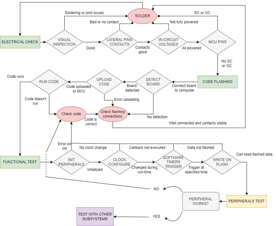
The SSV of the OBC consists of two main components: hardware and software.
Hardware Validation
The hardware validation begins with an electrical check. The first step is to visually inspect the soldered board for marks, scratches, significant soldering errors, and other potential issues. Next, the lateral pins of the board are evaluated for poor contacts.
Once all contacts are confirmed, voltages are measured, and MCU pins are checked for potential shorts or open circuits. If the hardware is deemed properly set up, the software evaluation phase begins. It is essential to ensure that the MCU can run user-uploaded code. At this stage, new potential points of failure include the flashing connections and the uploaded code.
After successfully running simple code on the MCU, the next step is to evaluate the initialization of various mission-critical peripherals. This includes on-the-fly clock reconfigurations, which may occur during the mission, and confirming that software timer triggers occur at the specified times. It is also critical to verify that writing to flash memory is possible. Following these steps, the peripherals are tested, and integration with other subsystems is performed to further verify proper behavior.
Software Development and Validation
At every stage of software development, different strategies are employed to validate progress. The initial steps involve using a Nucleo STM L4746RG Development Board. Since most subsystems rely on the MCU and the power line, both of which can be easily emulated, the software for each subsystem is first tested on a system composed of the Nucleo and the hardware to be validated.
In the early iterations, a bare-bones approach is taken, delaying the implementation of the software into the FreeRTOS environment until the hardware is validated. Once the software is adapted and integrated into the RTOS, the unit to be verified consists of the previous hardware and the software as a single FreeRTOS task. Note that some subsystems require values read from sensors for verification. To address this, numerical approximations of these values are used to simplify testing.
Once a subsystem is confirmed not to be a source of problems, it is integrated with the actual OBC-COMMS board for further testing. This integration may be facilitated by the EGSE (FlatSAT) or through manual connections, depending on the system.
During subsequent validation phases, the unit under test expands to cover the full system or as much as is reasonably testable. This includes integrating the remaining subsystems, both in hardware and software. The modular approach of the system facilitates comprehensive verification. FlatSAT testing is crucial during this phase, as it provides a suitable platform for system-level software tests.
Final Validation Steps
The final steps involve verifying the software under the environmental conditions the satellite will encounter. This process encompasses the entire system and simulates these conditions using various facilities and tools.
To support communication with the external environment for control and debugging purposes, the satellite is equipped with two communication mechanisms. The first is an umbilical cable, which facilitates the transmission of output logs generated by the satellite and allows for command input via a wired connection. The second method utilizes RF through the communications antenna, enabling command transmission in a manner consistent with real operational scenarios.
Tests as Run
DOCUMENT SCOPE
The aim of this document is to clearly explain the tests performed during the delevolpment of the subsystem.
This document is based on current but also previous versions both of hardware and software and as such be followed with care.
TEST 1: Electrical check
Test Description and Objectives
The aim of this test is to verify that non of the components or connections had been damaging during the assembling, and that the consumption of the components is nominal.
Requirements Verification
| Requirement ID | Description |
|---|---|
| OBC-001 | There must be no visible damage to the board, such as scratches, soldering or joint issues. |
| OBC-011 | Each pin found in the lateral sides must have good electrical connection |
| OBC-012 | Verify that there are not any shorts, nor open ends, and the corresponding behavior and value |
| OBC-021 | The board must be powered with 3.3 V and all the power pins from the board must be checked |
| OBC-031 | All the other pins from the board must be electrically checked in order to make sure that the board is responding correctly |
Test Set-Up
- OBC payload full soldered
- Microscope
- Power Supply
- Wires
- Soldering machine
- Tin
- Flux
- Multi-meter
- Calculator, pen and paper
- Laptop with KiCad and the design
Pass/Fail Criteria
The PCB will be verified if the five requirements mentioned before are fulfilled. If in one of them it is detected any anomaly it will have to be corrected, otherwise the board can not pass to the other tests.
Test Plan
- With the help of the microscope, look at the PCB looking for any outer physical parameters, such as scratches, soldering or joint issues. If any anomaly is detected, re-solder or fix the encountered error.
- Check the correct connection with the corresponding component of the 40 pins (10 in each lateral side) with the multi-meter.
- Check the value with the multi-meter of all the passive components and compare it to the one in the schematic.
- Verify the active components, checking one by one all the pins with the multi-meter in order to find shorts, open ends, and correct connections among the various pins.
- Check the connections between all of the components and pins of the PCB
Test Results
The test for the EPS PCB has been done during the 01/06/2023.
The test passed the visual inspection since the outer physical checking was successful.
The pins', passive and active components' connectivity were successfully accomplished considering that there were no open ends or shorts, and the component values were correct.
The in-circuit testing was passed since the connections between all of the components and pints of the PCB were verified.
Anomalies
During the examination of the PCB no anomalies were detected.
Conclusions
The PCB passed the electrical test and is ready to do more complex tests.
TEST 2: In-circuit voltages
Test Description and Objectives
The objective of this test is to verify that when providing the PCB with the power supply, the voltages and currents are correct on the whole PCB
Requirements Verification
The voltages required for each component are summarized in the following chart (they can be seen from the datasheet of each component):
| COMPONENT | Vin Min (V) | Vin Max (V) | Vo Min (V) | Vo Max(V) |
| SX1262IMLTRT | 1.8 | 3.7 | - | - |
| BGS12PL6E6327XTSA1 | 1.65 | 3.6 | - | - |
| STM32L476RGTx | 1.71 | 3.6 | - | - |
| BD2232G-GTR | 2.7 | 5.5 | -0.3 | Vin + 0.3 |
Test Set-Up
- OBC payload
- Microscope
- Multimeter
- Power supply unit
- Wires
- Pen and paper
- Computer with KiCad and the design
Pass/Fail Criteria
This test will be verified if the voltage obtained in the measurements of each component of the PCB is between the expected values.
Test Plan
- Prepare the power supply with 3.3V
- Connect the power supply to the PCB (3V3_PERM and GND)

- With the help of the multimeter, check that the inputs pins has the 3.3V value

With the help of the multimeter, check the voltage levels in the input and output of each component of the 3.2 chart
(the previous mentioned components are shown in order in the figures below, where the input put are marked in red)


Test Results
This test for the EPS PCB has been done during the 01/06/2023.
| COMPONENT | Vin (V) |
| SX1262IMLTRT | 3.35 |
| BGS12PL6E6327XTSA1 | 3.32 |
| STM32L476RGTx | 3.27 |
| BD2232G-GTR | 3.34 |
As it can be seen in the previous chart, all the components have the correct input voltage. The test has been correctly passed.
Anomalies
No anomalies has been detected
Conclusions
The PCB passed the test and is ready to do more complex tests.
TEST 3: STM32L476RG Flashing
Test Description and Objectives
The objective of this test is to verify that it is possible to flash code to the STM32L476RG using the ST-Link v2
Requirements Verification
| Requirement ID | Description |
|---|---|
|
OBC-101 |
The program ST-Link Utility must detect the STM32L476RG |
|
OBC-111 |
The STM32 must be able to run code |
|
OBC-121 |
A very simple instruction with a visible result must be written in order to prove that the code works correctly |
Test Set-Up
- OBC payload
- Microscope
- Multimeter
- ST-Link V2
- Saleae
- Wires
- Pen and paper
- Computer with KiCad, ST-Link Utility and Saleae
Pass/Fail Criteria
This test will be verified if the two requirements are fullfiled.
Test Plan
- Connect the ST-Link V2 to the OBC board


- Open the ST-Link utility program
- Connect the ST-Link V2 to the PC
- Click in the connection option and check if the program detects the STM32L476RG
- Open the STM32CubeIDE
- Debug code to see if the program detects the STM32L476RG
- Flash code


4.5.1 Debbuging steps for STM32 SWD Connection
ST-Link V2 connected to PC?
Yes
Connections ok? Revise ST-Link V2 and STM32 custom board SWD connections
Connection ok** **
**

STM32CubeIDE debbuger configured ok?

Supply ok? Check voltages
- Power Supply: 3.3V ok
- VCC PIN 1 STM: 3.3V ok
- VCC PIN 13 STM: 3.3V ok
- VCC PIN 19 STM: 3.3V ok
- VCC PIN 32 STM: 3.3V ok
- VCC PIN 48 STM: 3.3V ok
- VCC PIN 64 STM: 3.3V ok
ST-Link V2 ok? Try programming Nucleo board with ST-Link V2d
STM32 detects the nucleo board. Therefore, the ST_Link v2 is ok.

Signals and logic ok? Connect Saleae to SWD and NRST in STM32 custom board
The SWDO and the SWCLK are working ok, but no signal is received from the NRST PIN. The same happens when the Saleae is connected directly to the STM32.
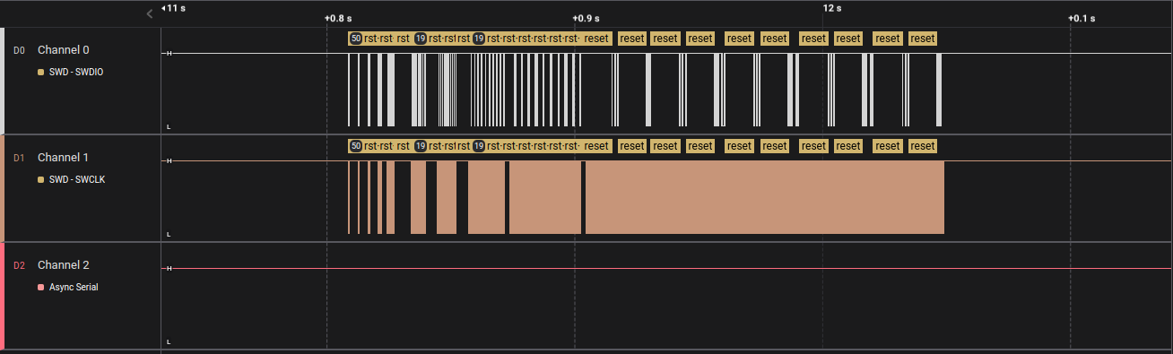
Signals from ST-Link V2 ok? Connect Saleae to SWD and NRST in ST-Link V2. Check if NRST is being aserted
Prepare STM32 board with minimum connections, only supply, gnd and SWD, does it work?
No, the ST-Link still does not detect the STM32
Resolder the board
When resoldering the board a mistake was detected: The STM32 has two orientation marks, and it was placed in the wrong direction. It is important to know that the hole that indicates the direction of the STM32 is the small one:

With the STM32 well orientated and the new PCB resoldered, the ST-Link can now make a connection with the STM32L476RG and flash code into it.
Test Results
This test for the OBC PCB has been done during the 02/06/2023.
The STM32L476RG was succesfully detected by the ST-Link Utility program

The STM32CubeIde also detected the STM32 and was able to run code through it.

Anomalies
When trying to do the connection with the ST-Link utility program, the STM32 was no detected. The debugging process realized to solve this problem can be seen in 4.5.1.
Conclusions
The PCB passed the test.
TEST 4: STM32L476RG functional test
Test Description and Objectives
The aim of this test is to verify that the required functions of the OBC can be performed by the STM32L4 integrated.
Requirements Verification
| Requirement ID | Description |
|---|---|
|
OBC - 211 |
The peripherals must be able to be correctly initialized |
|
OBC - 212 |
The clock has been able to be configured |
|
OBC - 221 |
FreeRTOS must be able to create a task |
|
OBC - 222 |
FreeRTOS must be able to do task scheduling |
|
OBC - 223 |
FreeRTOS must be able to make queue inter-tasks communication |
|
OBC - 224 |
It is needed to write on memory flash |
|
OBC - 225 |
The clock configuration can be changed during run-time |
|
OBC - 231 |
Be able to do software timers triggering (in 80, 26, 8 and 2 MHz) |
Test Set-Up
- OBC payload
- ST-Link V2
- Wires
- Pen and paper
- Computer with KiCad, ST-Link Utility and Saleae
- STM32CubeIDE with OBC code
Pass/Fail Criteria
The PCB will be verified if the five requirements mentioned before are fulfilled. If in one of them it is detected any anomaly it will have to be corrected, otherwise the board can not pass to the other tests.
Test Plan
- Connect the OBC to the ST-Link using the SWDIO connection
- Connect the ST-Link to the computer
- Run the code, implemented by Nil Rius, for the OBC
- Verify the correct initialization of the peripherals and the clock
- Check the task management list provided by FreeRTOS in order to verify the correct task creation and management.
- Use the FreeRTOS' functions to write in memory and look in the memory map to veirfy the correct writing.
- Verify that when the code changes the frequency of the clocks, the timer triggers at the correct time
Test Results
The test for the OBC PCB has been done during the 10/06/2023.
All the requirements have been successfully met.
Anomalies
During the examination of the PCB no anomalies were detected.
Conclusions
The PCB passed the STM32 functional test.
TEST 5: I2C reading of Temperature Sensor data test
Test Description and Objectives
This test is designed to attempt communication from the OBC-COMMS board, via I2C, to the TCN75A temperature sensor located on all of the lateral boards.
Requirements Verification
| Requirement ID | Description |
|---|---|
|
OBC-311 |
The sensor must be powered using the Nucleo board's output. |
|
OBC-312 |
Using the Nucleo, the configuration register of the temperature sensor must be set (TX). |
|
OBC-313 |
Using the Nucleo, the temperature data from the sensor must be received and tracked using PuTTY for a cleaner reading of the data (RX). |
|
OBC-321 |
The sensor must be powered using the output from the ST-Link/V2 programmer. |
|
OBC-322 |
The already written and tested code from the Nucleo must be correctly flashed onto the OBC-COMMS board using the ST-Link/V2 programmer. |
|
OBC-323 |
Using the OBC-COMMS board, the configuration register of the sensor must be set (TX). |
|
OBC-324 |
Using the OBC-COMMS board, the temperature data from the sensor must be received (RX). |
|
OBC-331 |
The temperature reading function must be defined and integrated in the main code from GitHub. |
|
OBC-332 |
The complete GitHub code, including the newly written function, must be flashed onto the OBC-COMMS board using the ST-Link/V2 programmer. |
|
OBC-333 |
Using the already flashed OBC-COMMS board, it must be shown that the configuration and temperature data is still being sent and received through I2C when the previously integrated function is called in the main(). |
Test Setup
Necessary materials:
- Lateral board with the TCN75A temperature sensor and all the necessary components (as seen in the KiCad project);
- Nucleo-L476RG board;
- OBC-COMMS board;
- ST-Link/V2 programmer;
- 2 x 4.7k Ω resistors (for pull-up);
- USB - USB 2.0 cable;
- 10 pin Molex connector and 4 crimped cables;
- Normal F-M and M-M cables;
- Protoboard;
- Laptop with STM32CubeIDE, KiCad, PuTTY and Picoscope installed and at least one USB port;
- Multimeter and oscilloscope/Picoscope for testing.
The setup for the initial test with the Nucleo:

[Detailed schematic made in photoshop to be inserted at a later date]
The setup for the subsequent test with the OBC-COMMS board:

[Detailed schematic made in photoshop to be inserted at a later date]
Pass/Fail Criteria
All of the requirements mentioned before must be fulfilled. If any one of them is not satisfactorily carried out, the anomalies must be taken care of. This test is absolutely critical since this is the easiest peripheral for I2C communication testing and this protocol is used for most internal communication jobs, so it is mandatory that it works without a hitch.
Test Plan
6.5.1. Initial test with the Nucleo board
Step 1:
Build the previously shown setup. Make sure all of the connections are good and, using the multimeter, measure all of the relevant voltages (Power Pin, NRST, SWDIO, SWCLK, I2C SDA, I2C SCL) to make sure they reach around 3.3 V.
Step 2:
All code and software related stuff will be done in STM32CubeIDE, as it's the easiest and most reliable tools to use.
Write code for transmitting configuration settings to the configuration register of the sensor (thus testing TX) and receiving temperature data from the temperature register of the sensor (thus also testing RX).
Make sure you read the documentation data for the TCN75A sensor in particular, how it handles I2C communication and pay special attention to the way the address of the sensor is formatted, taking into account the particular configuration of resistors from the lateral board which define the last 3 bits of said address.
Step 3:
Flash the Nucleo board with the code you have written (look-up tutorial), open PuTTY, put in the parameters of your serial virtual COM port which gets created automatically from the Nucleo debugger (you can see it in Device Manager -> Port) and connect. Run the program and see if the data gets transmitted correctly. You can touch the sensor to warm it up and check if the temperature readings match.
Optional:
You can check the I2C SDA and SCL signals respectively with the oscilloscope/Picoscope you're using.
The Picoscope IDE also allows you to decode the 2 signals if both are connected, which should technically give you the same output as in PuTTY.
6.5.2. OBC-COMMS board test
Once you have made sure that you can communicate through I2C between the Nucleo board and the sensor, it's time to try it with the main OBC-COMMS board.
The steps you should follow are exactly the same:
Step 1:
Build the previously shown setup.
Step 2 (extremely important):
Create a new project and redo the pin configuration in order to match the KiCad project for the OBC-COMMS board.
In particular, the I2C pins are not PB8 and PB9, but PB6 and PB7.
The code until and including the main() can be copy-pasted in its entirety from the other project.
Step 3:
Flash the code from this new project on the OBC-COMMS board using the debugger and test the values for the relevant variables while debugging. Since the ST-Link/V2 does not create a virtual COM port, the easiest way to check if the I2C communication is correctly being performed is by debugging step by step and checking if the variables change according to how they're supposed to.
6.5.3. Temperature reading function definition, integration and testing with the full code
Now that the OBC-COMMS -> Temperature Sensor communication works, the only thing left to do is to create a function, integrate it in the full code and test its functionality as a whole.
One of the ways to do this is:
Step 1:
Decide in what subsystem you want to integrate this code. In this case, it would make the most sense to write a function in the ADCS subsystem, since everything related to the lateral board "depends" on the ADCS.
Step 2:
Write the function and its corresponding header. Make sure to include everything you need in the header, especially all files which contain the I2C functions.
The .c file will be basically the same as the other code, containing all the functions that the other one contains, and changing it so that the main() of the existing code is all contained inside a function that will be called in the main.c file in order to test if everything works as intended.
Step 3:
Call the previously brought up function in the main.c file of the program.
Repeat the setup from the previous test and flash the entire code on the OBC-COMMS board. While debugging, go step by step and when you reach the temperature sensor data reading function, click on "Step into", and again, go step by step and check the relevant variables to see if their values correspond with your expected outputs.
If everything is good and nothing in the code crashed unexpectedly, that means that the integration test was successful.
Test Results
6.6.1. Initial test with the Nucleo board
This is the code I wrote for the Nucleo board test (not including the autogenerated functions):
//* Includes ------------------------------------------------------------------*/
#include "main.h"
#include "i2c.h"
/* Private includes ----------------------------------------------------------/
#include <string.h>
#include <stdio.h>
#include <math.h>
/ Private typedef -----------------------------------------------------------/
/ USER CODE BEGIN PTD /
/ USER CODE END PTD */
/* Private define ------------------------------------------------------------*/
#define TCN75_ADDR 0x4C // Change as per your hardware configuration
#define REG_CONFIG 0x01
#define REG_TEMP 0x00
/* USER CODE BEGIN PD /
/ USER CODE END PD */
/* Private macro -------------------------------------------------------------/
/ USER CODE BEGIN PM /
/ USER CODE END PM */
/* Private variables ---------------------------------------------------------*/
I2C_HandleTypeDef hi2c1;
UART_HandleTypeDef huart2;
/* USER CODE BEGIN PV /
/ USER CODE END PV */
/* Private function prototypes -----------------------------------------------*/
void SystemClock_Config(void);
static void MX_GPIO_Init(void);
static void MX_USART2_UART_Init(void);
void MX_I2C1_Init(void);
/* USER CODE BEGIN PFP */
void I2C_ReInit(void);
HAL_StatusTypeDef I2C_CheckError(I2C_HandleTypeDef *hi2c, uint16_t DevAddress);
void I2C_BusReset(void);
void UART_Log(char message);
/ USER CODE END PFP */
/* USER CODE BEGIN 0 */
void I2C_ReInit(void) {
HAL_I2C_DeInit(&hi2c1);
MX_I2C1_Init();
}
HAL_StatusTypeDef I2C_CheckError(I2C_HandleTypeDef *hi2c, uint16_t DevAddress) {
if (HAL_I2C_IsDeviceReady(hi2c, DevAddress, 3, 1000) != HAL_OK) {
uint32_t errorCode = HAL_I2C_GetError(hi2c);
char errorMsg[64];
sprintf(errorMsg, "I2C Error: 0x%lx\r\n", errorCode);
UART_Log(errorMsg);
I2C_ReInit();
return HAL_ERROR;
}
return HAL_OK;
}
void I2C_BusReset(void) {
GPIO_InitTypeDef GPIO_InitStruct = {0};
HAL_I2C_DeInit(&hi2c1);
GPIO_InitStruct.Pin = GPIO_PIN_9 | GPIO_PIN_8;
GPIO_InitStruct.Mode = GPIO_MODE_OUTPUT_OD;
GPIO_InitStruct.Pull = GPIO_NOPULL;
GPIO_InitStruct.Speed = GPIO_SPEED_FREQ_HIGH;
HAL_GPIO_Init(GPIOB, &GPIO_InitStruct);
for (int i = 0; i < 9; i++) {
HAL_GPIO_WritePin(GPIOB, GPIO_PIN_8, GPIO_PIN_SET);
HAL_Delay(1);
HAL_GPIO_WritePin(GPIOB, GPIO_PIN_8, GPIO_PIN_RESET);
HAL_Delay(1);
}
MX_I2C1_Init();
}
void UART_Log(char message) {
HAL_UART_Transmit(&huart2, (uint8_t)message, strlen(message), HAL_MAX_DELAY);
}
int main(void) {
HAL_Init();
SystemClock_Config();
MX_GPIO_Init();
MX_USART2_UART_Init();
MX_I2C1_Init();
while (1) {
uint8_t buf[12];
int8_t val_bfc;
float val_afc = 0.0f;
uint8_t auxbuf[12];
char sign = ' ';
buf[0] = REG_CONFIG;
buf[1] = 0x60; // Example configuration value
char AuxilMsg[64];
sprintf(AuxilMsg, "While loop reset \r\n");
HAL_UART_Transmit(&huart2, AuxilMsg , strlen(AuxilMsg), HAL_MAX_DELAY);
if (I2C_CheckError(&hi2c1, TCN75_ADDR << 1) == HAL_OK) {
sprintf(AuxilMsg, "I2C OK \r\n");
HAL_UART_Transmit(&huart2, AuxilMsg , strlen(AuxilMsg), HAL_MAX_DELAY);
HAL_I2C_Master_Transmit(&hi2c1, TCN75_ADDR << 1, buf, 2, HAL_MAX_DELAY);
buf[0] = REG_TEMP;
sprintf(AuxilMsg, "First transmission complete \r\n");
HAL_UART_Transmit(&huart2, AuxilMsg , strlen(AuxilMsg), HAL_MAX_DELAY);
HAL_I2C_Master_Transmit(&hi2c1, TCN75_ADDR << 1, buf, 1, HAL_MAX_DELAY);
sprintf(AuxilMsg, "Second transmission complete \r\n");
HAL_UART_Transmit(&huart2, AuxilMsg , strlen(AuxilMsg), HAL_MAX_DELAY);
HAL_I2C_Master_Receive(&hi2c1, (TCN75_ADDR << 1) | 0x01, buf, 2, HAL_MAX_DELAY);
sprintf(AuxilMsg, "Receiving complete \r\n");
HAL_UART_Transmit(&huart2, AuxilMsg , strlen(AuxilMsg), HAL_MAX_DELAY);
if(buf[0] >= 0x80)
{sign = '-';
auxbuf[0] = buf[0] - 0x80;
auxbuf[1] = buf[1];
}
else
{
auxbuf[0] = buf[0];
auxbuf[1] = buf[1];
}
val_bfc = (uint8_t) auxbuf[0];
for (int i = 0; i < 8; ++i) {
if (auxbuf[1] & (1 << i)) {
val_afc += 1 / pow(2, 8-i);
}
}
val_afc *= 100;
char tempMsg[64];
sprintf(tempMsg, "Temperature: %c%d.%02d C\r\n", sign, val_bfc, (int)val_afc);
HAL_UART_Transmit(&huart2, (uint8_t*)tempMsg, strlen(tempMsg), HAL_MAX_DELAY);
} else {
UART_Log("I2C Error. Resetting...\r\n");
I2C_BusReset();
}
HAL_Delay(500);
}
}
And this is the specially created "i2c.h" file, which when the full integration test will be done will be placed in the "CommonResources" folder:
/*
* Created on: 02.12.2023
* Author: Vladimir Frunza
*/
/* Define to prevent recursive inclusion -------------------------------------*/
#ifndef __I2C_H
#define __I2C_H
#ifdef __cplusplus
extern "C" {
#endif
/* Includes ------------------------------------------------------------------*/
#include "stm32l4xx_hal.h"
/* USER CODE BEGIN Includes */
/* USER CODE END Includes */
extern I2C_HandleTypeDef hi2c1;
/* USER CODE BEGIN Private defines */
/* USER CODE END Private defines */
void MX_I2C1_Init(void);
/* USER CODE BEGIN Prototypes */
/* USER CODE END Prototypes */
#ifdef __cplusplus
}
#endif
#endif /* __I2C_H */
Flashing it on the board with the complete setup and reading the output from PuTTY, it looks something like this:

-> This is the sensor just measuring the background temperature;

-> This is the sensor heating up as I touch it;

-> And this is the sensor cooling down as I stop touching it.
This test is considered a success.
6.6.2. OBC-COMMS board test
As previously mentioned, it is extremely important to make sure that the pin configuration for each test is correct.
In our case, the difference between the Nucleo and the OBC-COMMS board is the location of the I2C pins:
The Nucleo uses pins PB9 and PB8 for I2C While the OBC-COMMS board uses pins PB7 and PB6 for I2C


Apart from this change, all the software (including the code) is exactly the same, since the 2 communicating devices (the MCU from the OBC-COMMS board and the temperature sensor) are identical.
Again, as previously mentioned, since the ST-Link/V2 doesn't create a virtual COM port, the easiest way to check is to check the relevant variables in the code by debugging step by step.
In my test, this looks like this:

The relevant values after going through the entire main() are val_bfc (value before the comma) and val_afc (value after the comma).
As you can see:
- val_bfc = 23, meaning that there are 23.xx °C;
- val_afc = 6.25, meaning that there are 23.06 °C.
This test is also considered a success.
6.6.3. Temperature reading function definition, integration and testing with the full code
Once everything else is done, this should be the easiest part. The only worries should be:
- To make sure that you're not blocking the rest of the processes that should be happening when running the full code;
- To make sure that you're including all the files needed and that you're not getting errors like "function not found/defined";
- To integrate your function in such a way that you do not get stuck in any infinite loop when running it or it doesn't add unexpected delays to the rest of the code, making some things not work unexpectedly.
From the code I wrote, this is the header for the .c file, both of which are contained in the ADCS subfolder:
/*
* Created on: 02.12.2023
* Author: Vladimir Frunza
*/
#ifndef __LATBOARD_TEMP_SENSOR_H
#define __LATBOARD_TEMP_SENSOR_H
#ifdef __cplusplus
extern "C" {
#endif
/* Includes ------------------------------------------------------------------*/
#include "stm32l4xx_hal.h"
/* Private includes ----------------------------------------------------------/
/ USER CODE BEGIN Includes /
#include "i2c.h"
#include "main.h"
/ USER CODE END Includes */
/* Private defines -----------------------------------------------------------/
#define TCN75_ADDR 0x4C
#define REG_CONFIG 0x01
#define REG_TEMP 0x00
/ USER CODE BEGIN Private defines */
/* USER CODE END Private defines */
#ifdef __cplusplus
}
#endif
#endif /* __LATBOARD_TEMP_SENSOR_H */
And this is the .c file, named in the same way as the header, "latboard_temp_sensor":
/*
* Created on: 02.12.2023
* Author: Vladimir Frunza
*/
//* Includes ------------------------------------------------------------------*/
#include "latboard_temp_sensor.h"
#include "i2c.h"
#include "main.h"
/* Private includes ----------------------------------------------------------/
#include <string.h>
#include <stdio.h>
#include <math.h>
/ Private typedef -----------------------------------------------------------/
/ USER CODE BEGIN PTD /
/ USER CODE END PTD */
/* USER CODE BEGIN PFP */
void I2C_ReInit(void);
HAL_StatusTypeDef I2C_CheckError(I2C_HandleTypeDef *hi2c, uint16_t DevAddress);
void I2C_BusReset(void);
void UART_Log(char message);
/ USER CODE END PFP */
/* USER CODE BEGIN 0 */
void I2C_ReInit(void) {
HAL_I2C_DeInit(&hi2c1);
MX_I2C1_Init();
}
HAL_StatusTypeDef I2C_CheckError(I2C_HandleTypeDef *hi2c, uint16_t DevAddress) {
if (HAL_I2C_IsDeviceReady(hi2c, DevAddress, 3, 1000) != HAL_OK) {
uint32_t errorCode = HAL_I2C_GetError(hi2c);
char errorMsg[64];
sprintf(errorMsg, "I2C Error: 0x%lx\r\n", errorCode);
UART_Log(errorMsg);
I2C_ReInit();
return HAL_ERROR;
}
return HAL_OK;
}
void I2C_BusReset(void) {
GPIO_InitTypeDef GPIO_InitStruct = {0};
HAL_I2C_DeInit(&hi2c1);
GPIO_InitStruct.Pin = GPIO_PIN_9 | GPIO_PIN_8;
GPIO_InitStruct.Mode = GPIO_MODE_OUTPUT_OD;
GPIO_InitStruct.Pull = GPIO_NOPULL;
GPIO_InitStruct.Speed = GPIO_SPEED_FREQ_HIGH;
HAL_GPIO_Init(GPIOB, &GPIO_InitStruct);
for (int i = 0; i < 9; i++) {
HAL_GPIO_WritePin(GPIOB, GPIO_PIN_8, GPIO_PIN_SET);
HAL_Delay(1);
HAL_GPIO_WritePin(GPIOB, GPIO_PIN_8, GPIO_PIN_RESET);
HAL_Delay(1);
}
MX_I2C1_Init();
}
void UART_Log(char message) {
HAL_UART_Transmit(&huart4, (uint8_t)message, strlen(message), HAL_MAX_DELAY);
}
void Send_Latboard_Temp(void)
{
uint8_t buf[12];
int8_t val_bfc;
float val_afc = 0.0f;
uint8_t auxbuf[12];
char sign = ' ';
buf[0] = REG_CONFIG;
buf[1] = 0x60;
char AuxilMsg[64];
//sprintf(AuxilMsg, "While loop reset \r\n");
//HAL_UART_Transmit(&huart2, AuxilMsg , strlen(AuxilMsg), HAL_MAX_DELAY);
if (I2C_CheckError(&hi2c1, TCN75_ADDR << 1) == HAL_OK) {
//sprintf(AuxilMsg, "I2C OK \r\n");
//HAL_UART_Transmit(&huart2, AuxilMsg , strlen(AuxilMsg), HAL_MAX_DELAY);
HAL_I2C_Master_Transmit(&hi2c1, TCN75_ADDR << 1, buf, 2, HAL_MAX_DELAY);
buf[0] = REG_TEMP;
//sprintf(AuxilMsg, "First transmission complete \r\n");
//HAL_UART_Transmit(&huart2, AuxilMsg , strlen(AuxilMsg), HAL_MAX_DELAY);
HAL_I2C_Master_Transmit(&hi2c1, TCN75_ADDR << 1, buf, 1, HAL_MAX_DELAY);
//sprintf(AuxilMsg, "Second transmission complete \r\n");
//HAL_UART_Transmit(&huart2, AuxilMsg , strlen(AuxilMsg), HAL_MAX_DELAY);
HAL_I2C_Master_Receive(&hi2c1, (TCN75_ADDR << 1) | 0x01, buf, 2, HAL_MAX_DELAY);
//sprintf(AuxilMsg, "Receiving complete \r\n");
//HAL_UART_Transmit(&huart2, AuxilMsg , strlen(AuxilMsg), HAL_MAX_DELAY);
if(buf[0] >= 0x80)
{sign = '-';
auxbuf[0] = buf[0] - 0x80;
auxbuf[1] = buf[1];
}
else
{
auxbuf[0] = buf[0];
auxbuf[1] = buf[1];
}
val_bfc = (uint8_t) auxbuf[0];
for (int i = 0; i < 8; ++i) {
if (auxbuf[1] & (1 << i)) {
val_afc += 1 / pow(2, 8-i);
}
}
val_afc *= 100;
char tempMsg[64];
//sprintf(tempMsg, "Temperature: %c%d.%02d C\r\n", sign, val_bfc, (int)val_afc);
//HAL_UART_Transmit(&huart2, (uint8_t*)tempMsg, strlen(tempMsg), HAL_MAX_DELAY);
}
else {
//UART_Log("I2C Error. Resetting...\r\n");
I2C_BusReset();
}
}
As you can see, the function that will be called in the main.c file is "Send_Latboard_Temp()", function which is almost a one to tone copy of the while(1) loop from the int main() of the previous program.
After including the "latboard_temp_sensor.h" in the "adcs.h" file which is included in the "main.h" file and calling the previously mentioned function in int main() of main.c, by stepping into it after debugging we can see:

At the end of the execution of the function, the previously talked about val_bfc and val_afc have the values 22 and 56.25 respectively, meaning a temperature of 22.56 °C.
Considering that everything else after the end of the execution of this functions runs as it should, meaning all tasks and all timers are created correctly, we can say that this test is also a success, meaning the absolute goal was accomplished.
Anomalies and mistakes
Making everything work for this test took considerably longer than expected, and here is a list of problems I faced that anyone who tries I2C communication should also consider and thoroughly verify:
1. Connection issues
Be it either cables being damaged, boards being improperly soldered, connectors not touching or any other one of these very common problems, I2C like any other communication protocol requires a strong and well defined signal, especially when trying to communicate something as delicate as an exact temperature value, where even a bit flip can have dramatic consequences.
The only real way to make sure that you're not experiencing any connection issues is to painstakingly check every possible connection by hand, firstly with a simple multimeter in order to make sure that your voltages are correct, and then with an oscilloscope in order to more finely analyze the signals transmitted.
Separating each connection and testing it individually is always better than trying to test everything when it's all connected, since there can be a lot of broken links in a bigger chain and it's way harder to identify which one is problematic.
2. Unfamiliar connectors
When working on any electronics project, you might very quickly come to see a component of any kind with which you are unfamiliar. In that case, instead of trying to work your way around a functionality of said component, it is always better to use it as it is intended, since that is the optimal way to make sure that you are not shooting yourself in the foot.
In our case, the lateral board has a 10/11 pin connector which requires special crimping of cables with a specialized Molex crimping tool in order for the connection to be strong. Trying without crimping has led quickly led me to the conclusion that, even though there might be a connection, for something like I2C a poor connection is as good as no connection.
3. Burned or damaged components
Every board that requires soldering is subject to damage: damage of the copper traces, damage of the lateral connectors, damage of the components, etc.
Sometimes it is better to make manually make sure that all your components are in working condition and that the connections between them are not damaged than just assume that's the case and have to suffer the potential consequences. Other times, changing them anyway might even be the safer strategy.
4. Mistakes in the basic setup of the experiment
Be it either a mistake in the physical setup, the setup in the IDE or even a big gap in the logic of the code itself, these mistakes are extremely common and do happen to everyone.
The only way to prevent this is to check even the things that you consider to be the most basic and logical things from the get go. Read all the documentation for the chips you are using, thoroughly consult all the schematics for the circuits that you are using and never assume that if something worked in a specific way with a board that it should work exactly the same with another one.
Conclusions
The I2C testing of the temperature sensor from the lateral boards was a complete success and now we can be sure that we have an OBC-COMMS board with working I2C pins that is ready for further testing of the peripherals.
TEST 6: ADCS gyroscope data read with OBC
Test Description and Objectives
The aim of this test is to verify that the OBC payload can establish a correct communication with the ADCS board and receive data from the gyroscope.
Requirements Verification
| Requirement ID | Description |
|---|---|
|
OBC-411 |
The ADCS board must be powered using the Nucleo board's output. |
|
OBC-412 |
Using the Nucleo, the I2C communication between the gyroscope and the MCU must be established, and the data must be correctly transmitted. |
|
OBC-421 |
The ADCS board must be powered using the ST-Link/V2 output. |
|
OBC-422 |
The ADCS board and the OBC board should be able to communicate data from the gyroscope to the MCU through I2C. |
|
OBC-431 |
The gyroscope reading function must be defined and integrated in the main code from GitHub. |
|
OBC-432 |
The complete GitHub code, including the newly written function, must be flashed onto the OBC-COMMS board using the ST-Link/V2 programmer. |
|
OBC-433 |
Using the already flashed OBC-COMMS board, it must be shown that the I2C communication between the chips still works when the previously integrated function is called in the main(). |
Test Setup
This is the list of required materials for this test:
- ADCS board
- OBC-COMMS board
- ST-Link/V2
- Power Supply
- Wires
- 2 x 4.7k Ω resistors (pull-up)
- Multimeter
- Oscilloscope
- Calculator, pen and paper
- Laptop with STM32CubeIde and Ki-Cad installed
Pass/Fail Criteria
The test will be verified if the requirements mentioned before are fulfilled. If in one of them it is detected any anomaly it will have to be corrected, otherwise the board can not pass to the other tests.
Test Plan
7.5.1. The Nucleo board test
This is a picture of the setup for the Nucleo board test:

To complete this test, the following steps should be followed:
Step 1: Connect the 3.3V pin to the ADCS PCB.
Step 2: With the help of the multimeter, check that the VCC inputs pins has the correct value.
Step 3: Connect the Nucleo's SCL and SDA pins to the ADCS's corresponding I2C 3 pins.
Step 4: Prepare a code that can read from the gyroscope using I2C
Step 5: Run the code into the Nucleo and debug it step by step to see if the communication between the Nucleo and the ADCS has been done.
7.5.2. The OBC-COMMS board test
This is a picture of the setup:

These are the steps to follow:
Step 1: Connect the power supply from the ST-Link/V2 to the ADCS PCB and OBC PCB
Step 2: With the help of the multimeter, check that the VCC inputs pins has the correct value
Step 3: Connect the OBC payload to the computer using SWDIO pins
Step 4: Prepare a code that can read from the gyroscope using I2C
Step 5: Connect the OBC to the ADCS PCB using SCL and SDA pins
Step 6: Run the code into the OBC and look in the memory register to see if the communication between the OBC and the ADCS has been done.
Test Results
This is the code used for the Nucleo - ADCS data read test:
/* Includes ------------------------------------------------------------------*/
#include "main.h"
#include "iim42652.h"
#include "Sumador.h"
#include <string.h>
#include <stdio.h>
#include <stdlib.h>
/* Private includes ----------------------------------------------------------/
/ USER CODE BEGIN Includes /
int buf[100];
/ USER CODE END Includes */
/* Private typedef -----------------------------------------------------------/
/ USER CODE BEGIN PTD */
/* USER CODE END PTD */
/* Private define ------------------------------------------------------------/
/ USER CODE BEGIN PD */
/* USER CODE END PD */
/* Private macro -------------------------------------------------------------/
/ USER CODE BEGIN PM */
/* USER CODE END PM */
/* Private variables ---------------------------------------------------------*/
I2C_HandleTypeDef hi2c1;
UART_HandleTypeDef huart2;
/* USER CODE BEGIN PV */
/* USER CODE END PV */
/* Private function prototypes -----------------------------------------------/
void SystemClock_Config(void);
static void MX_GPIO_Init(void);
static void MX_USART2_UART_Init(void);
static void MX_I2C1_Init(void);
/ USER CODE BEGIN PFP */
/* USER CODE END PFP */
/* Private user code ---------------------------------------------------------/
/ USER CODE BEGIN 0 */
/* USER CODE END 0 */
/**
-
@brief The application entry point.
-
@retval int
/
int main(void)
{
/ USER CODE BEGIN 1 /
uint8_t GyroState=1;
uint8_t ValidData=1; // 1=true,0=false
/ USER CODE END 1 */
/* MCU Configuration--------------------------------------------------------*/
/* Reset of all peripherals, Initializes the Flash interface and the Systick. */
HAL_Init();
/* USER CODE BEGIN Init */
/* USER CODE END Init */
/* Configure the system clock */
SystemClock_Config();
/* USER CODE BEGIN SysInit */
/* USER CODE END SysInit */
/* Initialize all configured peripherals /
MX_GPIO_Init();
MX_USART2_UART_Init();
MX_I2C1_Init();
/ USER CODE BEGIN 2 */
IIM_init(&hi2c1);
IIM_configGyro(SET_GYRO_FS_SEL_15_625_dps, SET_GYRO_ODR_1kHz);
/* USER CODE END 2 /
//float degreesx=0,degreesz=0,degreesy=0,temperature=0;
iim_raw_data data;
iim_scaled_data scaled_data;
iim_averaged_data averaged_data;
CircularQueue queueX,queueY,queueZ;
int8_t average_samples=10;//10=1 seg
int counter=0,full=0; //full=1 databuffer full
/ Infinite loop /
/ USER CODE BEGIN WHILE /
int databuf_size=100;
float databuffer[databuf_size];
uint8_t capacity=queue_compute_capacity(0.1,1);
queue_init(&queueX,&queueY,&queueZ,capacity);
while (1)
{
/ USER CODE END WHILE */
/* USER CODE BEGIN 3 */
IIM_readGyro(&data);
IIM_convertGyro(&scaled_data,data,GyroState);
IIM_readTemperature(&data.temperature);D
IIM_ChangeState_Gyro(&data,&scaled_data,&GyroState,&ValidData);
HAL_Delay(100);
if(ValidData==1){
average_algorithm(&scaled_data,&averaged_data,&queueX,&queueY,&queueZ);
sprintf((char*)buf,"%d %d %d %d \r\n",data.x,data.y,data.z,data.temperature);
HAL_UART_Transmit(&huart2, buf, strlen((char*)buf), HAL_MAX_DELAY);
}
}
/* USER CODE END 3 */
}
INITIAL TESTING
Unfortunately, the ADCS board I worked with could not correctly flash this code, since there were issues with the 2 I2C pins who constantly remained at 0 V.
Even though I have briefly tried to figure out what the problem could be, it seems like there are more things wrong with that board.
That being said, Edgar Hernandez Recio, the ADCS responsible who wrote the code from above, did manage to flash and correctly transmit gyroscope data through I2C with this code, using another board.
So, this test is a success, but it will need replicating if I want to test the OBC-COMMS -> ADCS communication, most likely with the only ADCS board that seems to work.
FURTHER TESTING
After I changed the ADCS board from the one that obviously wasn't working to Edgar's working board and working together with him in order to make sure that we have the correct software configuration inside the IDE (correct code + correct pinout), we managed to replicate the Nucleo board test with my laptop, resulting in a complete success of test 1.
After that, I changed the configuration to the one for the OBC-COMMS test, again worked with Edgar to ensure that everything is as intended, and managed to communicate through I2C between the OBC-COMMS board and the ADCS board, resulting in a complete success of test 2 and, by proxy, the entire experiment.
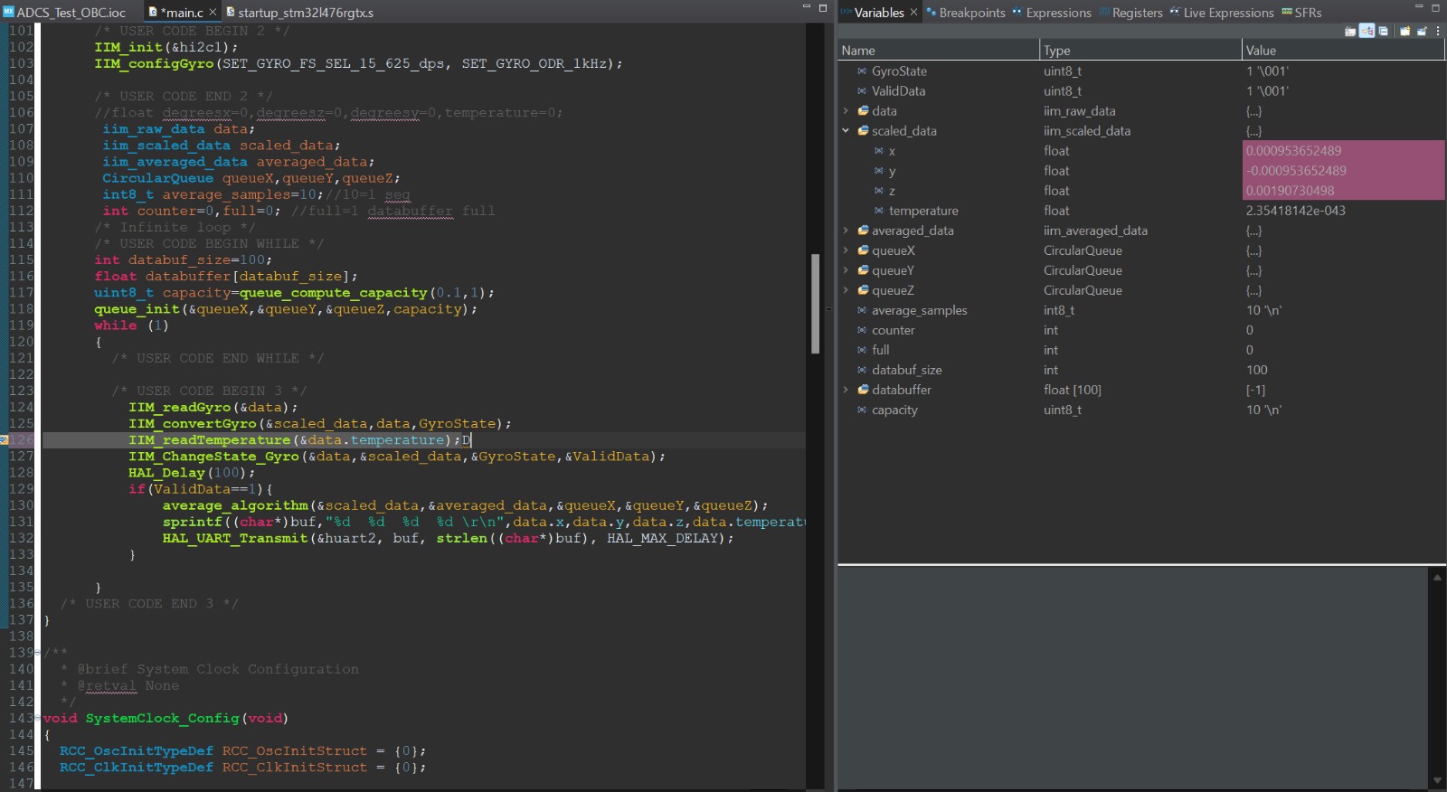
This is how a correct non-moving test with correct values is supposed to look. All of the 3 values from the 3 axis of the gyroscope are pretty much 0, indicating complete stillness.
Anomalies
The biggest anomaly that we faced is that only one of the ADCS boards we have is fully operational.
This could be due to many factors, some of the most likely culprits being:
- bad soldering;
- burned components;
- bad connectors.
In order to increase the efficiency of the workflow, the recommendable thing to do is fix at least one of the non-working ADCS boards, as to enable multiple people testing with ADCS at the same time. The best solution to doing this is to completely resolder new components from scratch, since that is the only way to ensure that everything will be working as intended.
Conclusions
The ADCS gyroscope data read test was a complete success, so that means that we can continue with the peripheral testing and also have the certainty that at least one ADCS board is fully operational.
TEST 7: ADCS photodiode data read and ADC data converting with OBC
Test Description and Objectives
The aim of this test is to verify that the OBC which was previously shown to be able to establish a correct communication with the ADCS board can also correctly read data from the photodiode, meaning that both the photodiode itself and the Analog to Digital Converter must work as intended.
Requirements Verification
| Requirement ID | Description |
|---|---|
|
OBC-511 |
The ADCS board and lateral board must be powered using the Nucleo board's output. |
|
OBC-512 |
Using the Nucleo, the I2C communication between the photodiode and the MCU must be established and the data must be correctly transmitted once it has been converted by the ADC. |
|
OBC-521 |
The ADCS board and lateral board must be powered using the ST-Link/V2 output. |
|
OBC-522 |
The ADCS board, the OBC board and the lateral board should be able to communicate data from the photodiode through I2C and the readable data correctly converted by the ADC. |
|
OBC-531 |
The photodiode reading function must be defined and integrated in the main code from GitHub. |
|
OBC-532 |
The complete GitHub code, including the newly written function, must be flashed onto the OBC-COMMS board using the ST-Link/V2 programmer. |
|
OBC-533 |
Using the already flashed OBC-COMMS board, it must be shown that the I2C communication between the chips still works when the previously integrated function is called in the main(). |
Test Setup
This is the list of required materials for this test:
- ADCS board
- OBC-COMMS board
- Lateral board with a photodiode
- ST-Link/V2
- Powerful halogen lamp
- Power Supply
- Wires
- 2 x 4.7k Ω resistors (pull-up)
- Multimeter
- Oscilloscope
- Calculator, pen and paper
- Laptop with STM32CubeIde and Ki-Cad installed
Pass/Fail Criteria
The test will be verified if the requirements mentioned before are fulfilled. If in one of them it is detected any anomaly it will have to be corrected, otherwise the board can not pass to the other tests.
Test Plan
This is the picture of the necessary setup (and a cameo by Artur):
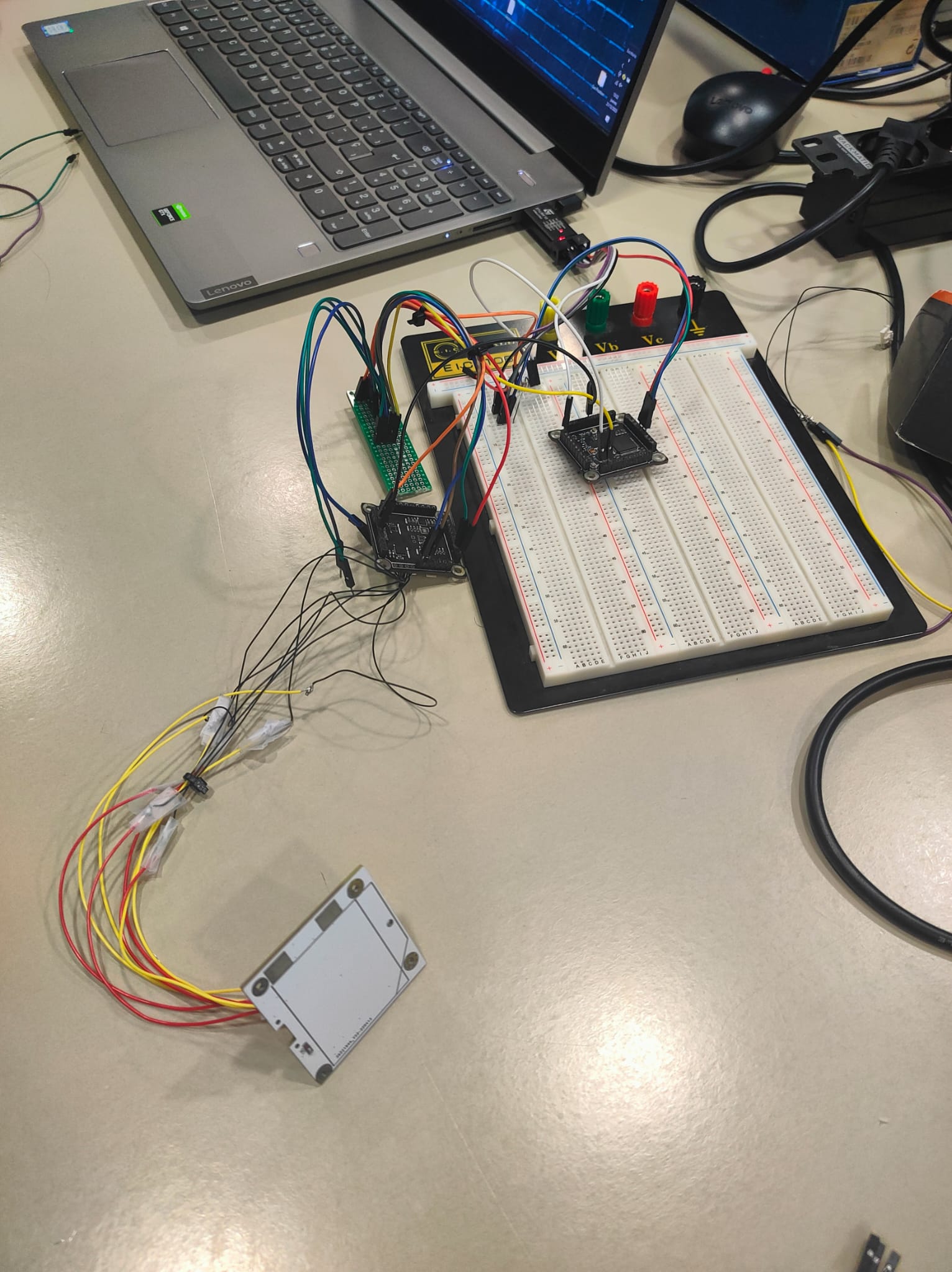
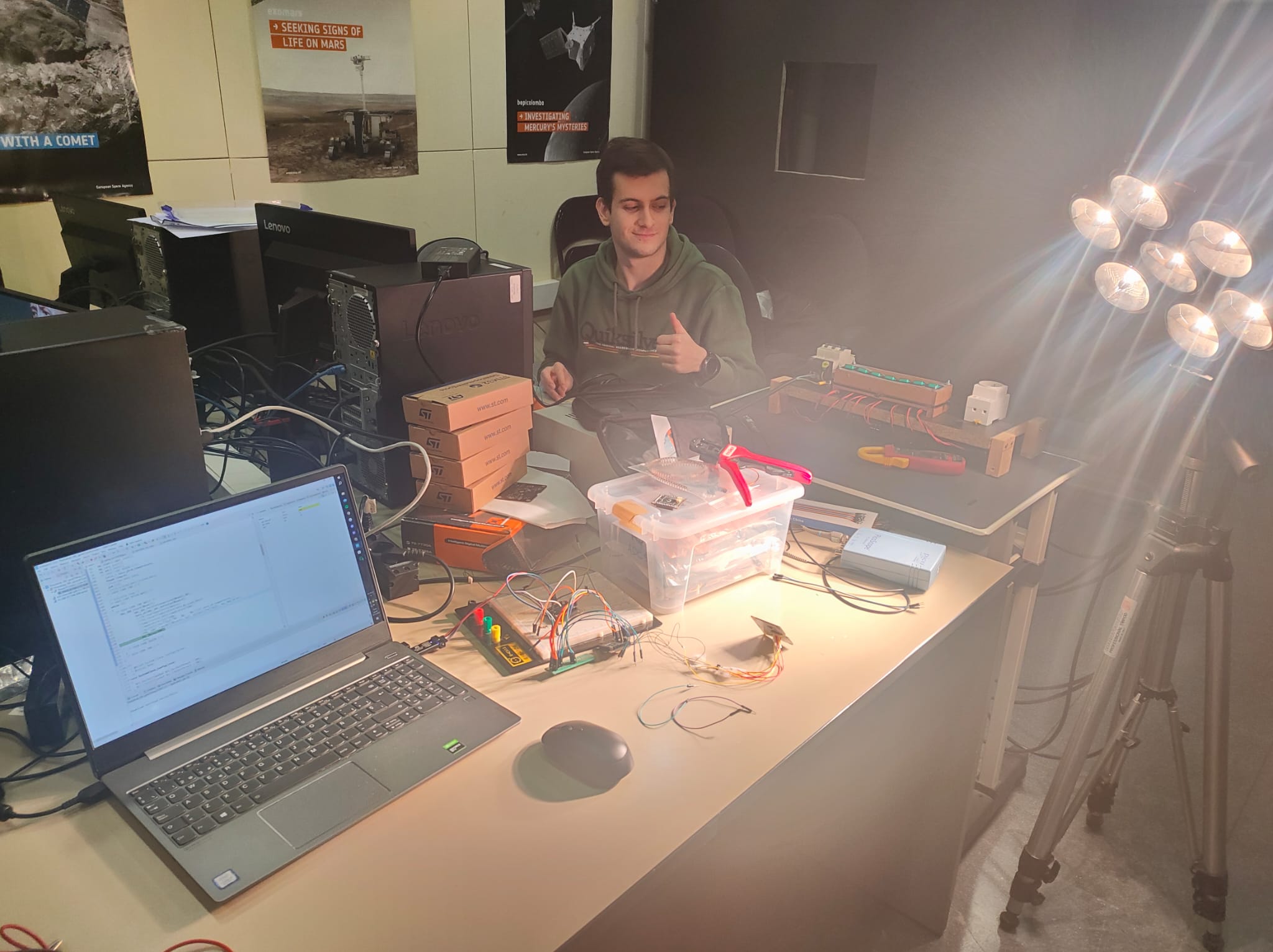
These are the steps to follow:
Step 1: Connect the power supply from the ST-Link/V2 to the ADCS PCB, OBC PCB and lateral board.
Step 2: With the help of the multimeter, check that the VCC inputs pins has the correct value
Step 3: Connect the OBC payload to the computer using SWDIO pins
Step 4: Prepare a code that can read from the photodiode using I2C
Step 5: Connect the OBC to the ADCS PCB using SCL, SDA and ADC-PH pins
Step 6: Connect the lateral board with the ADC-PH pin to the same pins from the 2 PCBs
Step 7: Run the code into the OBC and look in the memory register to see if the communication between the OBC and the ADCS has been done.
Test Results
This is the code used for the OBC-ADCS photodiode and ADC test:
#include "main.h"
/* Private includes ----------------------------------------------------------/
/ USER CODE BEGIN Includes /
int buf[100];
/ USER CODE END Includes */
/* Private typedef -----------------------------------------------------------/
/ USER CODE BEGIN PTD */
/* USER CODE END PTD */
/* Private define ------------------------------------------------------------/
/ USER CODE BEGIN PD */
/* USER CODE END PD */
/* Private macro -------------------------------------------------------------/
/ USER CODE BEGIN PM */
/* USER CODE END PM */
/* Private variables ---------------------------------------------------------*/
ADC_HandleTypeDef hadc1;
I2C_HandleTypeDef hi2c1;
UART_HandleTypeDef huart2;
/* USER CODE BEGIN PV */
/* USER CODE END PV */
/* Private function prototypes -----------------------------------------------/
void SystemClock_Config(void);
static void MX_GPIO_Init(void);
static void MX_USART2_UART_Init(void);
static void MX_I2C1_Init(void);
static void MX_ADC1_Init(void);
/ USER CODE BEGIN PFP */
/* USER CODE END PFP */
/* Private user code ---------------------------------------------------------/
/ USER CODE BEGIN 0 */
/* USER CODE END 0 */
/**
- @brief The application entry point.
- @retval int
/
int main(void)
{
/ USER CODE BEGIN 1 */
/* USER CODE END 1 */
/* MCU Configuration--------------------------------------------------------*/
/* Reset of all peripherals, Initializes the Flash interface and the Systick. */
HAL_Init();
/* USER CODE BEGIN Init */
/* USER CODE END Init */
/* Configure the system clock */
SystemClock_Config();
/* USER CODE BEGIN SysInit */
/* USER CODE END SysInit */
/* Initialize all configured peripherals /
MX_GPIO_Init();
MX_USART2_UART_Init();
MX_I2C1_Init();
MX_ADC1_Init();
/ USER CODE BEGIN 2 /
int16_t data_ph=0,temperature;
float temp=0;
//tcn_raw_data data;
int i=1;
//tcn_scaled_data scaled_data;
/ USER CODE END 2 */
/* Infinite loop /
/ USER CODE BEGIN WHILE /
while (1)
{
/ USER CODE END WHILE /
HAL_ADC_Start(&hadc1);
HAL_ADC_PollForConversion(&hadc1,20);
data_ph=HAL_ADC_GetValue(&hadc1);
//TCN_readTemperature(&data);
//TCN_convertTemperature(data,&scaled_data);
//temp=(scaled_data.temperature100);
//temperature=(int)temp;
//sprintf((char*)buf,"%d %d %d \r\n",data_ph,temperature,i);
//HAL_UART_Transmit(&huart2, buf, strlen((char*)buf), HAL_MAX_DELAY);
HAL_Delay(100);
i++;
/* USER CODE BEGIN 3 /
}
/ USER CODE END 3 */
}
TEST RESULTS
After a few usual connection issues, the test went smoothly from what was basically the first attempt. Having a halogen lamp with multiple modules, we could test the reading with a lot of different settings, and we found that the number of modules that are lit is almost proportional to the value we read, meaning the test was in fact a success. Below are the results for 3 different light readings: no lights, 2 lights and 7 lights. The relevant variable is "data_ph", marked in yellow since it has just changed value.

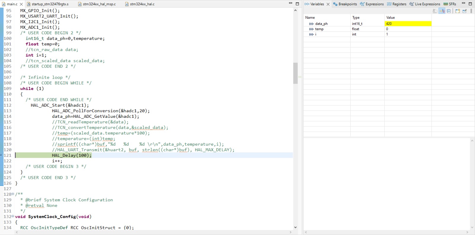
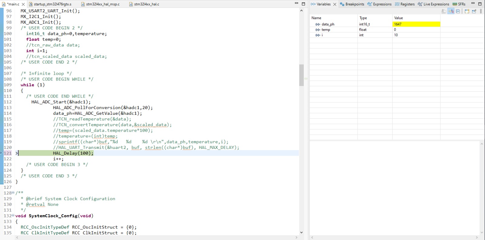
Anomalies
In this test, apart from the usual connection issues, we encountered no notable anomalies.
Conclusions
The ADCS-OBC photodiode data read and ADC data converting test was a complete success, meaning we have managed to test another one of the functionalities of the system and that we are getting closer to a fully integrated system test.