Electrical Power System (EPS)
- Subsystem Description
- Hardware Design
- Software Design
- Subsystem Verification (SSV)
- Tests as Run
- Tests as Run (Legacy)
Subsystem Description
Functional Architecture
The EPS is responsible for managing the energy throughout the satellite, including charging the battery and distributing power to the various subsystems. It is divided into two main blocks: the Energy Harvest Block, which is in charge of collecting energy from the solar cells and maximizing power generation, and the Battery Charger Block, which efficiently and safely charges the LiPo battery while distributing power to the different subsystems.
It is made use of a total of 5 solar cells: 4 on the sides and 1 on the bottom. These are high-efficiency GaAs triple junction solar cells with an efficiency rate of 30%. The solar cells on the sides are arranged in parallel (+Z with -Z and +X with -X). This configuration allows one of the two faces to always be illuminated, enabling the use of one MPPT (Maximum Power Point Tracker) for each pair of solar cells. The bottom cell is managed individually with its own MPPT.
The MPPTs are responsible for maximizing the power generated by the solar cells. After the MPPT output, with a reverse-blocking diode, the power management system will handle the energy distribution.
The Power Management IC is the core component that manages energy at all times, deciding the actions based on the available energy and the requirements of the other subsystems. Depending on the battery’s charge state, the Power Management IC will take advantage of the opportunity to charge it, ensuring that energy is always available.
Simultaneously, energy is constantly sent through a power regulator, reducing the voltage to 3.3V, which is used by the other subsystems. The Power Management IC will decide whether to power the system directly from the solar cells, depending on the power consumption, or from the battery when necessary.
The EPS also includes a battery sensor capable of measuring various battery parameters such as voltage, current and temperature. This sensor communicates with the OBC via I2C. Additionally, the battery is equipped with an NTC temperature sensor that the Power Management IC can read to ensure the battery does not overheat or drop below a certain threshold. If the OBC detects that the battery temperature approaches a critical level, it will activate a battery heater to maintain the temperature within safe operating limits
Moreover, the Power Management IC, through digital control pins, will notify the OBC of its status, including notifications such as charge completed or battery error, among others.
To the other subsystems, the EPS appears as a single power source, capable of providing the necessary energy at all times while also supplying real-time battery data.
A block diagram of the EPS is provided up next:

Figure 1: EPS Block Diagram
Requirements
The EPS is designed and schedulled tu fulfill the following requirements established by the necessitities of the spacecraft and the mission itself.
| SS | SS - Number | DESCRIPTION |
|---|---|---|
| EPS | EPS-0000 | The EPS is capable of providing the requisite current for the other subsystems to function correctly. |
| EPS | EPS-0010 | The battery shall remain within safe temperature ranges. |
| EPS | EPS-0020 | The EPS shall provide an output of 3.3V ±5% at its output to power the other subsystems |
| EPS | EPS-0030 | The battery shall be able to charge via the umbilical port. |
| EPS | EPS-0040 | The satellite's battery shall be decoupled from the rest of the system during launch using mechanically controlled kill switches. |
| EPS | EPS-0050 | The EPS shall charge the battery automatically using the solar cells. |
| EPS | EPS-0060 | The EPS shall include protections to prevent battery damage |
| EPS | EPS-0070 | The MPPTs shall produce sufficient power to charge the battery |
Hardware Design
Design Choices
Up next is provided a table including the most important components of the EPS. In the following sections is found information about each one of them as well as the overall design of the system.
Quick Facts Table
| Component | Model |
|---|---|
| Solar Cell | Lightricity S3040_CIC |
| Battery | 3.7v 1400 mAh |
| MPPT | SPV1040TTR |
| Power Management | LTC4040 |
| Battery Sensor | DS2782E+ |
| Voltage Regulator | ISL9120IRTNZ |
| MOSFET | SIR424DP-T1-GE3 |
Table 1: EPS main components.
Solar Cells
The selected model is the S3040_CIC from Lightricity, a 30% Triple Junction Gallium Arsenide and Ultra High-Efficiency solar cell. Note that due to a recent shortage of supplies from the solar cell provider, it was necessary to seek alternatives and switch to a new provider and model. Consequently, certain values, parameters, and renders are still being defined and are in the process of being updated. The cells were chosen due to their availability as well as their capability to meet al requirements established.

Figure 1: Lightricity S3040CIC (Solar array)
The following tables show the main specifications of S3040_CIC solar arrays and their physical dimensions:
| Lightricity S3040CIC | |
|---|---|
| Integration | CIC (Coverglass Interconnected Cells) |
| Size (mm) | 40.15 × 30.35 × 0.30 |
| PV active area | 12cm² |
| Voltage output (AM0) | ~ 2.5V |
| Power Output (AM0) | ~ 0.5W |
Table 2: Solar array main specifications.
Note that the array has Coverglass Interconnected Cells (CIC), a specific type of solar cell assembly used in space-grade solar panels. The term refers to a system in which individual solar cells are interconnected and covered with a thin protective glass layer.
Also notice that both voltage output and power output is presented at AM0, which indicates the measures are given at Air Mass Zero, outside the Earth's atmosphere, therefore without it's filtering.
PV active area indicates the area of the array in which the photovoltaic efect is produced.
The solar array dimensions and physical properties are provided in Table 3:
| Dimensions | |
|---|---|
| Max. length L (mm) | 40.15 |
| Max. width W (mm) | 30.35 |
| Total thickness (µm) | 300 |
| Coverglass thickness (µm) | 100 |
| Interconnector (Ag) thickness (µm) | 25 |
| Total cell area (cm²) | 12 |
| Total weight (mg/cm²) | <120 |
Table 3: Solar array dimensions
In the next tables the electrical parameters are presented, both at the Beginning of Life (BOL) and at End of Life (EOL). Then an explanation is given of each one.
| Main electrical parameters | BOL | EOL (10^15 e.cm^-2) |
|---|---|---|
| Voc (V) | 2.74 | 2.48 |
| Jsc (mA.cm^-2) | 17.2 | 16.7 |
| Vmp (V) | 2.45 | 2.26 |
| Jmp (mA.cm^-2) | 16.4 | 15.4 |
| Efficiency (%) | >30.0 | 25.7 |
Table 4: Solar cells main electrical parameters
| Thermal coefficients | BOL | EOL (10^15 e.cm^-2) |
|---|---|---|
| dVoc / dT (mV.°C^-1) | -5.9 | -6.2 |
| dJsc / dT (µA.cm^-2.°C^-1) | 14.8 | 14.6 |
| dVmp / dT (mV.°C^-1) | -6.5 | -6.9 |
| dJmp / dT (µA.cm^-2.°C^-1) | 9.9 | 10.1 |
Table 5: Solar cells thermal coeficients
Voc (Open-circuit voltage) indicates the maximum voltage produced by the cell when exposed to sunlight but not connected to a load, this parameter presents a variation of around -6 mV for each increase of a temperature degree. Jsc (Short-circuit current density) corresponds to the maximum current density produced by the cell when shortcurcuited, with a variation of around -15 µA/cm^2 for each degree incease.
Vmp and Jmp indicate the maximum value of these parameters when power is at its maximum. Both have a variation of the same order as the aforementioned corresponding ones.
Lateral & Bottom Boards
The lateral boards have an area of 23 cm^2, while the solar cells have an active area of 12 cm^2. Thus, 52% of the lateral board area is occupied by the solar cells. Regarding the bottom PCB, its area is 33.3 cm^2, and the solar cells occupy 36% of this area. The payload section has a surface area of approximately 20.1 cm^2, but it does not contain any solar cells.
In conclusion, solar cells cover 41% of the total exterior surface area of the PocketQube. Each solar cell 3.52 has four pins: two on the top, one in the corner, and the last one on the entire backside. When mounted on the lateral board, the solar cell will be soldered by its back pin and the three top pins. The attachment of the solar cells to the PCB will rely on these solder joints, especially as the backside of the solar cell is a large pad, providing sufficient soldering area to secure the cell properly.

Figure 2: Image of the solar cell pins
Each lateral board and bottom board has one solar cell each. The cells are soldered to the PCBs in such a way that they remain securely attached without the need for adhesives or additional supports. In the following Figures 3 and 4, we can see that there are four soldering pads: two blue pads representing the negative pads, and the red pad covering the entire back of the solar cell, which corresponded to the positive pad. Additionally, the green pad located in the upper left corner is associated with the By-Pass diode.

Figure 3: Solar Cells Placement
The By-Pass diode in solar cells is essential for series connections, ensuring that if one cell fails, the others remain unaffected. However, in our spacecraft, parallel connections are used, making the By-Pass diode unnecessary. If required, connecting the negative pad to the diode pad would suffice, as shown in Figure 4.

Figure 4: Solar Cell By-Pass diode placement and connection
Battery
When selecting a battery for the satelite, it is essential to choose one with the highest possible capacity that can still fit within the space constraints.
The battery selected is a 3.7 V 1400 mAh LiPo battery, with a size of 42 x 35 x 10 mm and a weight of 23.4g , and was chosen for the following reasons:
- Energy Efficiency: The battery operates between 3.7V and 4.2V. Since the system runs at 3.3V, reducing the voltage to 3.3V is more efficient than stepping it up.
- Temperature Tolerance: LiPo batteries can handle extreme temperature fluctuations, which is crucial for space environments. However, charging is restricted to temperatures above 0 ◦C, and operation is limited to certain ranges. If not regulated, improper temperatures can lead to battery failure. However, the EPS’s integrated circuit will help manage this to prevent potential failures.
- PocketQube Compliance: The selected battery adheres to the PocketQube standard in terms of both size and weight, making it an ideal option.
- Depth of Discharge: For a mission lifespan of 2.7 years (approximately 15,100 cycles, given a 94-minute orbital period), the battery’s discharge rate per cycle is a key factor. Ensuring proper discharge control is crucial for longevity.
In the next table the electrical parameters of the battery are presented:
| Parameters | Value |
|---|---|
| Part Number | LP 103438 |
| Nominal Voltage | 3.7V |
| Nominal Capacity | 1400mAh |
| Internal Impedance | <60mΩ |
| Charge Voltage | 4.2V |
| Recommended Charge Current | 0.2C |
| Allowed Max Charge Current | 0.5C |
| Output Voltage Range | 2.5V - 4.2V |
| Recommend Discharge Current | 0.2C |
| Max Continuous Discharge Current | 1C |
| Pulse Discharge Current | 3C (10ms) |
| Discharge Cut-off Voltage | 2.5 ± 0.05V |
| Cycle Life to 80% Health | 500 (0.2C, 25 °C) |
Table 6: Battery electrical parameters
The battery will be enclosed within a PTFE structure, ensuring it is well-secured and protected from potential impacts during satellite operation. The enclosure is designed not only to secure the battery but also to minimize the risk of fragment release in the event of a battery explosion. It provides a containment barrier, preventing fragments from escaping and damaging other satellite components.

Figure 5: Battery PTFE structure
Also in case the battery swells due to overheating, this structure allows for slight expansion while preventing excessive swelling.
The battery also includes several features designed to prevent damage to both the battery, and to the satellite. It incorporates an IC (G3R) and a MOSFET (CJ8810) on an internal board, which provide this protection. If the voltage drops to 3.0 V, the battery will automatically disconnect protecting against overdischarge. Similarly, if the charging voltage reaches 4.28 V, it will automatically disconnect to protect against overcharging. Additionally, thanks to these components, it also offers protection against short circuits and overcurrents by temporarily cutting off the output, preventing damage to both the battery, and to the satellite
MPPT
The MPPTs are responsible for maximizing the power generated by the solar cells. The STMicroelectronics SPV1040 was chosen due to it being able supports a parallel connection between the multiple solar array axes and having great efficiency. Another reason was because the manufacturer also provides simulation tools (eDesignSuite) that can be used for both dimensioning the biasing elements, as well as obtaining characteristics describing the current application. This greatly simplifies the development process and avoids potential design incompatibilities or errors.
The SPV1040 has an efficiency of up to 95% which minimizes energy losses from the solar cells, providing an output from the Energy Harvest Block between 0.3 and 5.5 V. This is critical due to the present power constraints.
Further information on the MPPT's can be found in their correspondant datasheet:
Power Management IC
The power management IC chosen was the Analog Devices LTC4040. This component was chosen because it offers control over the battery operation and is interfaceable with the On-Board Computer through basic logic pins. Moreover, the chip also offers a few safety features, in order to prevent damage that can be inflicted by over-currents, over-voltages and temperatures exceeding our established limits.
Some other notable feautures that made the decision clear are:
- Automatic switch from the solar power operation to battery operation, with the option of manual operation
- Battery-only power-up of the chip
- NTC Battery temperature monitoring and operation control
- Adjustable output current limiter
- Adjustable charging current (depending on the output current demand)
- Buck regulator for the battery charger
- Boost regulator for the battery discharger
- Faults and status output flags
Battery Sensor
The battery sensor chosen is the Analog Devices DS2782E+ it was selected due to its capacity to measure voltage, temperature and current, and estimate available capacity for rechargeable lithium-ion polymer batteries.
EPS Voltage Regulator
The voltage regulator chosen is the ISL9120IRTNZ, with up to 98% efficiency, it provides a constant output voltage of 3.3 V with a maximum current of 800mA. Since the battery produces between 3.7 V and 4.2 V, the regulator will reduce the voltage to 3.3 V, which is more energy-efficient than increasing the voltage.
A factor in the decision of selecting this part was the efficiency of the devide under the current conditions requiered by the PocketQube. The next figure ilustrates the effecinecy dependancy on consumption:

Figure 6: Voltage regulator efficiency
This regulator is also designed to prevent errors in any subsystem from impacting the battery and vice versa. It includes features such as over-temperature protection and undervoltage lockout. The over-temperature protection mechanism disables the device if the chip temperature exceeds 150°C, automatically reactivating it once the temperature falls to 115°C. Meanwhile, the undervoltage lockout function prevents the regulator from operating when the input voltage is too low, thereby ensuring the system functions correctly and safeguarding both the circuit and the battery.
Umbilical Voltage Regulator
The umbilical connector allows for battery charging, ans so this process is to be controlled and regulated by Texas Instruments TPS7A7002 a high-performance, positivevoltage, low-dropout (LDO) regulator. The devide was chosen due to its featuring of ultra-low dropout, useful as the input voltage through the connector is close to the charging voltage of the battery.
Schematic Design
The hardware schematic represents the subsystem connections between components as well as all the inputs and outputs in a clear, easy to work with, manner. This section will begin with the schematic of the different blocks and components of the EPS, ending with a general view of the whole design.
Energy Harvest Block
The energy harvest block main compontents are the solar cells as well as the MPPTs, providing an efficient power generation block, and, to ensure the integrity and safety of these components, a Schottky diode, avoid potential power returns to the block. The MPPT connections and components schematic was generated by eDesignSuite. The next figure is the block schematic:

Figure 7: Energy Harvest Block Schematic.
Note that there is a difference bewtween the generated design and the one used. This is the change of the 6x4.7uF capacitors at the input of the MPPTs in exchange for a single 1.5uF. Observe that the only inputs are the solar panels powers and the output is the regulated voltage at around 4.4V (the battery charges at 4.2V).
Power Management IC **
The charging/discharging operations of the battery are managed and performed by the power management IC, the central piece of this subsystem block. To understand the schematic it is convenient to have clear how the main IC works:
If there is a high enough voltage (programmable) at its input, then it will output the input, while charging the battery from the same power. As the current demand on the load increases, the chip automatically decreases the battery charging current. The battery is charged through a buck regulator to step down the voltage to the selected battery charging voltage. The charging voltage can be selected using the F0,F1 and F2 pins as such:

Table 7: PM IC Control Voltages
As the satellite enters the eclipse and the voltage output by the MPPTs decreases, the chip will automatically switch to discharging the battery.
The design followed corresponds to the reference application provided by the manufacturer but set up for our necessities. The schematic is presented in the next figure and then explained: 
Voltage Regulator
The voltage regulator is a buck-boost switching regulator that, in our case, will take as an input a voltage higher than the one it supplies as an output. The design chosen coincides with the typical design provided by the manufacturer, with the bypass mode deactivated, leaving the buck-boost mode on.

Figure 9: Voltage Regulator schematic
Battery Sensor
The battery sensor communicates through I2C with the OBC (SCL1,SDA1). It takes as inputs the battery poles and provides measures of it's temperatura, voltage, current and an estimation of capacity. The schematic is provided up next, guided by the manufacturers instructions:

Figure 10: Battery Sensor Schematic
Solar Cell Connections
The Solar Cells are located in the outer boards and interface with the lateral Picoblade connector:

Figure 11: Solar Cell Outer Board Connections Schematic.
Note that this circuit is located in the outer boards.
Killswitches
The killswitches remain pressed when inside the deployer and are only released when the PocketQube is ejected. While only one would be necessary two are chosen for redundancy and symmetry. They are connected to the positive pole of the battery and ensure no power is provided by it when pressed.
The schematic is provided next:

Figure 12: Killswitches Schematic.
Note that this circuit is located in the bottom board.
Charging Protections (Umbilical Voltage Regulator)
The umbilical connector allows for battery charging. This proccess is regulated and protected by the TPS7A7002, and the schematic follows the usual design presented by the manudacturer. It takes as an input the charging power from the connector and yields power to the battery as its only output.
The schematic is provided next:

Figure 13: Umbilical Charge Voltage Regulator Schematic.
Note that this circuit is located in the bottom board.
EPS Schematic Overview


Figure 11: EPS PCB Schematic Overview
PCB Design
EPS Board
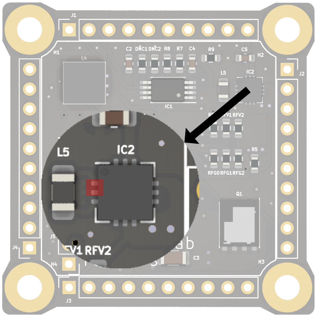
The EPS PCB is structured so that the different blocks are easily identifiable and accessible for maintenance. If we take a look at the PCB, we can see that the back Figure 12 is dedicated to the Energy Harvest Block, which contains only the MPPTs. Here, we can observe that all three MPPTs are connected in parallel, and despite they being identical, it should be easy to identify possible errors during testing. On the front Figure 12, the rest of the components are located. We can see that the part related to the Power Management IC is highlighted in red, the in battery monitor IC in blue , and the Voltage Regulator in green.

Figure 12: Views of the EPS PCB
The Energy Harvest Block is placed on the bottom layer of the PCB. Three identical blocks are placed in parallel receiving the power from the X (2 cells array), Y (2 cells array) and Z (single cell array) solar cells through the vertical connectors. The design tries to maximize compactness and cleanness in order to facilitate testing while making sure a failure in a single solar array does not become critical to the power integrity of the system.
The Power Management IC block has the main IC (LTC4040EUFD#PBF) centered on the top layer of the PCB in order to minimize the distance between the IC and the components it controls, reducing power path resistance and minimizing voltage drops. Placing the IC in the middle also helps with thermal distribution as significant heat is generated through its operation. The rest of the deisng follows standard practices to minime voltage spikes, such as the placement of decoupling capacitors to ground and so on.
The battery monitor IC and the Voltage Regulator are located as close as possible to the vertical connectors and the corner of the PCB. As the voltage regulator can generate significant heat this desicion is intended to help heat dissipation by providing more cooling space. This placement also intends to reduce thermal interference to the power management IC.
Being close to the connectors means being close to entry points of the PCB, avoiding the issues of measuring after distribution in case of the battery monitor, and the issues of power distribution for the voltage regulator.
PCB Layers
The EPS PCB is comprised of the following layers:

Figure 13: EPS PCB Layers
Software Design
The EPS software is encapsulated within the EPS task. It's main functionality is providing the OBC with battery readings on it's voltage, current generated, capacity, temperature and charging status. The task will also indicate any error generated by the Power Management IC.
The OBC is interfaced to the battery sensor through an I2C line yet it also receives and outputs information to the PM IC, as previously stated:
| Pin | Input / Output | Digital / Analog | Description |
|---|---|---|---|
| !CHRG | O | Digital | During a battery charging cycle, !CHRG is pulled low until the charge current drops below C/8 when the !CHRG pin becomes high impedance |
| !Fault | O | Digital | Indicates charge cycle fault conditions during a battery charging cycle. A temperature fault or a bad-battery fault causes this pin to be pulled low. If no fault conditions exist, the FAULT pin remains high impedance. |
| !RST | O | Digital | This pin is pulled to ground by an internal N-channel MOSFET whenever the RSTFB pin falls below 0.74V |
| CLPROG | O | Analog | VSYS Current Monitoring Pin |
| CHGOFF | I | Digital | Disable Pin for the Battery Charge. Enables the charger when tied to ground and disables it when tied to a voltage avobe 1.2V |
| !PFO | O | Digital | Pulled to ground by an internal N-channel MOSFET when the PFI input is below the falling threshold of the power-fail comparator. |
Table 1: LTC4040EUFD#PBF Interfaces with the OBC. The I/O point of reference is the EPS board.
The first duty it is responsible for is the polling of the battery sensor (DS2782E+) for voltage, current and capacity. This IC is connected to the IC2 line 1 (SCL1,SDA1).
The second duty is to keep monitoring of the state of the power harvesting and battery charging process. The LTC4040EUFD#PBF battery manager provides the required information and its acquired by directly reading GPIOs (set to input in the MCU) and an ADC in the case of the CLRPROG pin. Those PINS are the ones present in table 1.
Once all this information has been acquired by the task it is then sent to the back of a FreeRTOS queue where it will be read by the OBDH Task and subsequently stored in the flash memory.
A block diagram of the modus operandi is provided next:

Figure 1: EPS Task Data Block Diagram
Subsystem Verification (SSV)
The EPS consists of two main blocks. The process begins by soldering the MPPTs, and with the help of a solar simulator, they are tested using a solar cell to ensure proper functionality and that the output is as expected.
Next, the Battery Charge Block is soldered, followed by a visual inspection and continuity test to ensure there are no short circuits. Using a power supply, it is verified that the battery can provide a steady 3.3V output at the EPS output. The same test is conducted with the solar cells.
A battery charging test is performed using the solar cells to confirm that the battery charges correctly. The battery sensor is checked to ensure it reads accurate values, and the I/O pins of the Power Management IC are tested for proper operation. Finally, it is verified that the output can supply power to a load through the EPS output.
Figure 1: EPS SSV Block Diagram
Tests as Run
Test Description and Objectives
The objective of these tests is to check the correct functioning of the EPS system in all its parts, to ensure correct management of the energy between the solar panels and the battery to ensure the correct management of the supply in the different subsystems.
This document is based on current but also previous versions both of hardware and software and as such be followed with care.
Main components
- MPPT block > SPV1040TTR
- Battery charge/discharge management > LTC4040EUFD#PBF
- Sensor battery > DS2782E+
- Voltage regulator 3.3V > ISL9120IRTNZ
- MOSFET > SIR424DP-T1-GE3
- LiPo Battery > DNK 103438
- 1600 -> LP103740 3.7V 1600mAh https://lipolbattery.com/LiPo-Battery-1000mAh+.html
- Datasheet and 3D model of our Lightricity s3040_CIC solar cell > https://satsearch.co/products/exa-solar-cells-30-40

EPS board soldering test
Test Description and Objectives
The objective of this test is to check all the components of the EPS board to ensure the correct connectivity of every component because solder SMD components it’s a little hard to visually analyze, for that reason we need to find some specific point that help us to ensure the connections
Requirements Verification
| Requirement ID | Description |
| EPS_reqBST00 | Check visually or with microscope some short-circuit or some pin without enough tin |
| EPS_reqBST10 | Check if all IC are orientated properly |
| EPS_reqBST20 | Check if there are continuity between (Vcc) & (GND) and (Killswith+) & (Batt-) |
Test Set-Up
- EPS completetly soldered
- Multi-meter with wires
- PC with KiCAD with the EPS project opened
First, to verify EPS_reqBST00 and EPS_reqBT10, we need to visually inspect the components, paying particular attention to checking for potential short circuits or tin bubbles. We especially focus on U4 (LTC4040), Q1 (SIR424DP), and IC2 (ISL9120IRTNZ).
We will check the input of the MPPTs, their output, the battery power input, and the EPS output, to ensure there are no short circuits
If we encounter a short circuit during any of these checks, we should search for and repair the issue. To do this, we will return to step EPS_reqBST00 and attempt to resolve the short circuit. Pay attention to any potential tin bubbles that may have remained between the pins of the ICs
Pass/Fail Criteria
This test will be considered passed if all the requirement verifications are completed successfully
If one of the requirements fails, we cannot consider the test passed. For the following steps, where we apply voltage to the ICs, we need to ensure that there are no short circuits and no visible soldering errors to avoid damaging the PCB
Test Plan
| Step ID | Description | Pass/Fail Criteria | Actual | Passed\[Y/N\] |
| EPS_testBT00 | Solder all EPS board |
Ensure to solder the correct components in the correct places |
EPS components have been soldered properly | Y |
| EPS_testBT10 | Visually inspect the soldering | Check for any solder bridges between pins that could cause a short circuit or any poorly soldered pins | Some pins with short circuits were found and resolved, and some tin bubbles were removed | Y |
| EPS_testBT20 | Check electrically for short circuits | If we confirm the specified short circuits in the Test Set-Up, we pass the test | I had a short circuit in Solar Y due to the diode D2 being reversed. The diode has been rotated, and now it no longer indicates a short circuit | Y |
Test Results
Two short circuits caused by tin bubbles have been cleaned on IC2 and one on the U4, which have finally been eliminated.
An error was made in the placement of a component in step EPS_testBT00, which we initially deemed as good. We overlooked the polarity detail. The diode was rotated, and with this, we can confirm that the short circuit has been eliminated.
Anomalies
No anomalies have been detected.
Conclusions
We have been able to verify that there are no short circuits in the EPS, so the first EPS board soldering test has been passed. Now, the next test will involve applying voltage, so it is important to ensure that there are no short circuits-
EPS Battery and MPPT Evaluation
Test Description and Objectives
The purpose of this test is to verify that the EPS functions correctly electrically by powering it in different ways and checking that the outputs are as expected. Prior to this, we check for any short circuits, so now we can safely power it knowing that there are no short circuits. However, this does not mean that there are no errors, and therefore, we could potentially damage a chip. That's why it's important to have thoroughly checked the PCB in the previous test to minimize the risk of damaging any components.
Requirements Verification
| Requirement ID | Description |
| EPS_reqBT00 | Verify that we can obtain a constant 3.3V output from the EPS using a power supply |
| EPS_reqBT10 |
Verify that we can obtain a constant 3.3V output from the EPS using a battery |
| EPS_reqBT20 | Check that the MPPTs function with a power supply |
| EPS_reqBT30 | Verify that the MPPTs function with the solar cells |
| EPS_reqBT40 |
Verify that we can obtain a constant 3.3V output from the EPS using the MPPTs and the solar cells |
Test Set-Up
- EPS completetly soldered
- Multi-meter with wires or osciloscope with probe
- Power Supply
- LiPo Battery
- Lighttricity solar cell
- Wires
First, we are going to desolder diodes D4, D5, and D6 in order to separate the MPPT from the rest of the electronics.
We are going to set the power supply to 3V and limit the current to 0.1A.
To test the MPPT, we need to connect the solar cells on the top side and perform measurements on the bottom side. The GND of the solar panels must be connected to the PCB GND

Then to test EPS with the battery, it's important to connect the battery in the correct location. We must not connect the battery negative to the GND, as they are not the same. The battery negative should go to the BATT-. The output of the EPS is the 3.3V output that will be seen by the other SSVs
Pass/Fail Criteria
This test will be considered passed if all the requirement verifications are completed successfully
If one of the requirements fails, we cannot consider the test passed, as this process is important to ensure the correct power supply for the other SSVs
Test Plan
| Step ID | Description | Pass/Fail Criteria | Actual | Passed\[Y/N\] |
| EPS_testBT00 | Apply between 2V and 3V to the input of Solar X and check the MPPT operation | Output Solar X should have a voltage higher than the input, around 4V | The output is 4.5V, therefore we can confirm that the MPPT is functioning | Y |
| EPS_testBT10 | Apply between 2V and 3V to the input of Solar Y and check the MPPT operation | Output Solar Y should have a voltage higher than the input, around 4V | The output is 4.6V, therefore we can confirm that the MPPT is functioning | Y |
| EPS_testBT20 | Apply between 2V and 3V to the input of Solar Z and check the MPPT operation | Output Solar Z should have a voltage higher than the input, around 4V | The output is 4.6V, therefore we can confirm that the MPPT is functioning | Y |
| EPS_testBT30 | Apply 4V from the power supply to the battery input (KillSwitch + and Batt -) | Check if we have a constant 3.3V output at the EPS (VCC and GND) |
The output is not 3.3V, so the battery regulator part is not working. Additionally, there is a slight whistle coming from the EPS |
N (6.1) |
If we pass all the tests, we will resolder diodes D4, D5, and D6 to test the MPPT with the rest of the power management circuit and repeat the test to ensure the correct functioning of all EPS components with MPPT and power management together.
Now, the output pins for testing the MPPT blocks will be the EPS OUT instead the Solar OUT because we have added the diode, which makes more sense. Furthermore, we will continue using the power supply to test the battery and solar components via the EPS output
| Step ID | Description | Pass/Fail Criteria | Actual | Passed\[Y/N\] |
|
EPS_testBT40 |
Apply a voltage between 2V and 3V to the input of Solar X and check if the output works with only this power input when we illuminate it with strong light | The EPS output (VCC and GND) should provide a constant 3.3V | The EPS output provides a constant 3.3V | Y |
|
EPS_testBT50 |
Apply a voltage between 2V and 3V to the input of Solar Y and check if the output works with only this power input when we illuminate it with strong light | The EPS output (VCC and GND) should provide a constant 3.3V | The EPS output provides a constant 3.3V | Y |
|
EPS_testBT60 |
Apply a voltage between 2V and 3V to the input of Solar Z and check if the output works with only this power input when we illuminate it with strong light | The EPS output (VCC and GND) should provide a constant 3.3V | The EPS output provides a constant 3.3V | Y |
|
EPS_testBT70 |
Apply 4V from the power supply to the battery input (KillSwitch + and Batt -) | Check if we have a constant 3.3V output at the EPS (VCC and GND) | The EPS output provides a constant 3.3V | Y |
If we pass all the tests, now we will replace the power supply with solar cells and a LiPo battery. This way, we will perform the test in the real scenario
First we will connect the Lighttricity solar cells to the solar cell inputs, and then the battery (taking care with the polarity) to the pins (Killswitch+ and Batt-)
| Step ID | Description | Pass/Fail Criteria | Actual | Passed\[Y/N\] |
|
EPS_testBT80 |
We connect the Lighttricity solar cell to the Solar X input and illuminate it with strong light | The EPS output (VCC and GND) should provide a constant 3.3V | The EPS output provides a constant 3.3V | Y |
|
EPS_testBT90 |
We connect the Lighttricity solar cell to the Solar Y input and illuminate it with strong light | The EPS output (VCC and GND) should provide a constant 3.3V | The EPS output provides a constant 3.3V | Y |
|
EPS_testBT100 |
We connect the Lighttricity solar cell to the Solar Z input and illuminate it with strong light | The EPS output (VCC and GND) should provide a constant 3.3V | The EPS output provides a constant 3.3V | Y |
|
EPS_testBT110 |
Connect the LiPo battery to the battery input | Check if we have a constant 3.3V output at the EPS (VCC and GND) | The EPS output provides a constant 3.3V | Y |
|
EPS_testBT120 |
Connect a solar cell illuminated with strong light, and also connect the battery at the same time | Check that the output of the EPS remains at a constant 3.3V even when it receives sufficient energy from both inputs (solar and battery) | The EPS output provides a constant 3.3V | Y |
In this example, we can observe that when we connect a small load like an LED to the EPS output, the LED lights up when we illuminate the solar cell with a strong light, in this case from a headlamp

We can also see the result when connecting the LiPo battery.
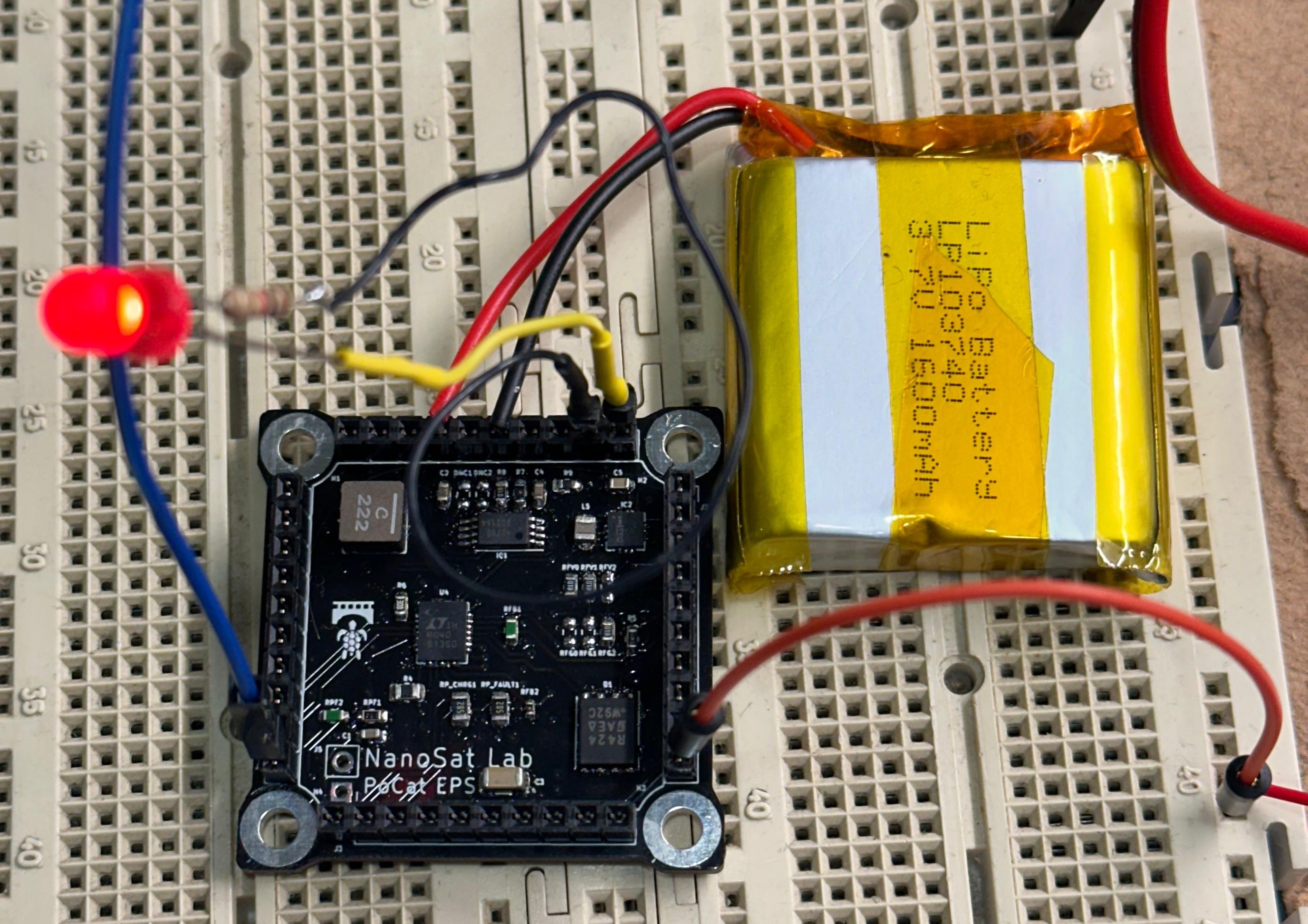
Test Results
We can confirm that we are able to provide a constant voltage of 3.3V at the output of the EPS using both the solar cells and the battery. Therefore, we will be able to properly power the different SSV either by solar light or by battery
6.1 EPS_testBT30
After checking that supplying 4V from the power supply to the EPS via the battery pins does not provide the expected constant 3.3V output, and additionally hearing a slight whistle from the PCB, we will review the PCB once more to identify any possible overlooked issues or visual signals that may provide clues.
We observe that the LX2 (1) and PGND (2) pins of the ISL9120IR regulator are short-circuited, so we proceed to remove the short circuit.
| Step ID | Description | Pass/Fail Criteria | Actual | Passed\[Y/N\] |
| EPS_testBT30 | Apply 4V from the power supply to the battery input (KillSwitch + and Batt -) | Check if we have a constant 3.3V output at the EPS (VCC and GND) | The output is a constant 3.3V. | Y |
Anomalies
If we illuminate the solar cells with classroom lighting or the flash of a mobile phone, we observe that the solar cell reaches 2V but is unable to activate the MPPT, thus it does not function. We require a more powerful light source, such as a headlamp, which also generates 2V from the solar cell but provides more current. So, we should not depend solely on the voltage reading from the solar cells to determine their operational status
Conclusions
Now, we have the MPPT working with the Lighttricity cells and the battery regulator as well. Therefore, we can now proceed with the next tests, as we can confirm that the generated voltages are correct.
Battery sensor test
Test Description and Objectives
The objective of this test is to check the correct functioning of battery sensor that provides to OBC some data about the battery like the Voltage, Current and Temperature.
Requirements Verification
| Requirement ID | Description |
| EPS_reqBS00 | Be able to read the battery voltage |
| EPS_reqBS10 | Be able to read the temperature of the battery using NTC |
| EPS_reqBS20 | Be able to read the actual current value |
| EPS_reqBS30 | Be able to read the average current value of the last 28s |
| EPS_reqBS40 | Be able to read the accumulated current value |
Test Set-Up
- 1x EPS board full soldered
- 1x STM32 Nucleo board
- 1x Power supply with 2 outputs
- 1x NTC sensor
- 1x Multi-meter or something with the capability to measure temperatures
- 1x Peltier cell to generate cold/hot temperatures or air hot gun
- 4x Banana-Banana power cables
- 1x LiPo battery
First, we will connect the EPS board to the STM32 Nucleo via I2C connection, and then connect the Nucleo to the STM32CubeIDE software.
Then we connect the NTC temperature sensor on EPS board, to modify the temperature we can use a Peltier cell that if we invert polarity will give us hot or cold as we need
Into the battery connector, we can connect a real LiPo battery or power supply.
The last is connect some kind of thermometer that gives us a real measurement of the read temperature of NTC sensor to compare with it.
Pass/Fail Criteria
This test will be considered passed if all of the following actions are performed successfully:
- If the read temperature is equal to the measured with external thermometer
- If the read voltage and current readings on sensor are equal with the showed on the power supply display or with a known value
On Standby
Tests as Run (Legacy)
Test campaign 2023-2
TEST PLAN- TESTS 1 - Communication with internal blocks
1. Test description and objectives
The purpose of this title is to verify the effective communication with the internal blocks of the EPS board and the OBC. This communication will be carried out using the I2C bus. The test is specifically aimed at reading the values of registers containing crucial data such as temperature, voltage, current and battery state of charge. To perform the test we will first use as OBC the STM32 board that we will use to read the registers of each chip separately and
Temperature measurement - DS2782E+
1- Test Description and Objectives
For this test, I utilized the STM32 board, the core-476RGD, with the aim of measuring the temperature through readings from the DS2782E+ chip via I2C communication. These measurements will be carried out by the OBC to monitor the system's temperature, ensuring the battery does not enter a charging state when it exceeds 45 degrees Celsius or when it falls below 0 degrees Celsius. In such cases, it can be hazardous as the battery may explode if it's in a charging state.
2 - Requirements Verification
3- Test Set-Up
The following materials were used:
- EPS board
- Two 4.7 kOhm resistors
- Cables for connections (male/male)
- Breadboard
- STM32 board (NUCLEO-l476RG)
- Cable for connecting STM32 with the PC
- PC with STM32cubeide software installed
Below, I present the board and the necessary connections for temperature readings:


4- Pass/Fail Criteria
Since the temperature must be between 0 and 45 degrees Celsius, under normal conditions, it's logical for it to be around 24 to 26 degrees Celsius. 13- Test Plan In this case, the EPS board is powered directly by the 3.3V supply from the STM32. To measure the temperature, we need to read registers 0x0A and 0x0B, the former for the most significant bits and the latter for the least significant bits. Each unit measured in this register represents 0.125 degrees Celsius. Below is an image representing the two registers to read, directly extracted from the DS2782 datasheet:

The code used is as follows:

5- Test Results
Satisfactory results were obtained, with temperature readings ranging from 23.25 ºC to approximately 29 ºC in multiple iterations. These values fall within the expected range. To ensure that the value varied with exposure to temperature changes, I conducted an experiment by, for example, placing the fingertip (previously discharged from static electricity), and the changes were gradual, with the temperature gradually increasing with each iteration of the I2C register read function. (The values for this test point were considered as floats).
An example of execution was as follows; after placing the fingertip, changes in the read value were observed:
6- Anomalies
No anomalies were found.
7- Conclusions
I must sieve and pass an integer instead of a float because transmitting that information to the OBC is more complicated using floats, and relevant information is lost. Therefore, based on the results, it is concluded that the DS2782E+ chip accurately measures temperature.
Voltage of the battery measurement - DS2782E+
1- Test Description and Objectives
Measuring the voltage is pivotal for understanding the battery's charge status, preventing overcharging or deep discharge, predicting battery life, and optimizing overall system performance by ensuring safe operations and maximizing battery lifespan.
2 - Requirements Verification
3 - Test Set-Up
The following materials were used:
- EPS board
- Two 4.7 kOhm resistors
- Li-on Battery for testing - 3.7 V / 1400mAh/5.18Wh - Model 103540
- Cables for connections (male/male)
- Protoboard
- STM32 board (NUCLEO-l476RG)
- Cable for connecting STM32 with the PC
- PC with STM32cubeide software installed


4 - Pass/Fail Criteria
According to the battery specifications and the voltage from the solar cells, the voltage range supported by the battery is from 0 to 4.25V with a maximum of 1A. The solar cells provide between 3.7V and 4.2V, fitting well within the correct voltage range. Regarding the current, at the SPV1040 output, there's an average of 250mA that can vary depending on the Maximum Power Point Tracking (MPPT), adjusting to the energy values received from the solar cells to maximize the power output.
5 - Test Plan
Code:

Running this function in the main.c while having Putty connected to COM3 port at a bus speed of 115200 bits/s will display the battery terminal voltage on the screen.
The registers that I measured are the next:

6 - Test Results
I've obtained an average result of 3.85 V. At times, it dropped to 3.7 V, but it never exceeded 4 V.
7 - Anomalies
No anomalies was found
8 - Conclusions
The voltage values measured at the battery terminals are correct as they fall within the typical operating range.
Current measurement - DS2782E+
1 - Test Description and Objectives
The objective of this test is to determine the current flowing through the battery using a 330-ohm resistor in the circuit, connected between Vcc and GND on the EPS board. This will allow us to assess how the battery discharges and verify if the current values do not exceed the allowed limit of 1 A. This type of measurement allows assessing the battery's charging and discharging efficiency while identifying potential anomalies in the energy flow. This is crucial to ensure optimal performance and safe management of the battery within the system.
2 - Requirements Verification
3 - Test Set-Up
Materials:
The following materials were used:
- EPS board
- Two 4.7 kOhm resistors
- 1 resistor of 330 Ohms
- Li-on Battery for testing - 3.7 V / 1400mAh/5.18Wh - Model 103540
- Cables for connections (male/male)
- Protoboard
- STM32 board (NUCLEO-l476RG)
- Cable for connecting STM32 with the PC
- PC with STM32cubeide software installed
We use the same setup as in the previous test, but this time placing a 330-ohm resistor between the Vcc and GND pins of the EPS board, which can be seen in this image:


4- Pass/Fail Criteria
According to the battery specifications, the current flowing through it should not exceed 1A; typically, we obtain values around 100 to 150 mA. When using a 330-ohm resistor, it's expected to yield readings around 10 mA. By verifying this, we can conclude that the measurement is accurate and acceptable within the electrical specifications of the devices involved.
5- Test Plan
With the configuration previously set up in the voltage test, connecting the battery to the EPS board and, in turn, to the NUCLEO-L476RG using I2C communication as in the previous cases, we can carry out the reading of the current registers.
Add the code that I wrote to read the registers that contain the current information. That registers are the next:

Code:

6- Test Results
The obtained result is 11.87 mA when a 330 Ohm resistor is connected between Vcc and GND.
7- Anomalies
Not found any anomalies
8- Conclusions
The result is as expected. In summary, we have successfully measured the discharge current flowing from the battery through the resistor. We can differentiate between input and output current based on whether the battery is charging or discharging, which is reflected in the sign of the measured value.
State of Charge of the battery measurement - DS2782E+
1 - Test Description and Objectives
This test aims to assess the accuracy and reliability of the State of Charge (SOC) measurement conducted by the DS2782E+ chip within the battery system. The objective is to verify whether the SOC readings align with the expected charge levels of the battery during various charging and discharging scenarios.
2 - Requirements Verification
3 - Test Set-Up
Materials:
The following materials were used:
- EPS board
- Two 4.7 kOhm resistors
- 1 resistor of 330 Ohms
- Li-on Battery for testing - 3.7 V / 1400mAh/5.18Wh - Model 103540
- Cables for connections (male/male)
- Protoboard
- STM32 board (NUCLEO-l476RG)
- Cable for connecting STM32 with the PC
- PC with STM32cubeide software installed
We use the same setup as in the current measurement case. Here, our connections will be similar, with the battery logically connected with the positive terminal at the kill switch and the negative terminal at BATT-.
4- Pass/Fail Criteria
Ensure that the battery capacity reading does not exceed the specified limits of 1400mAh. It should accurately represent the actual capacity and align with calculations derived from the SOC (State of Charge) and RARC (Remaining Standby Absolute Capacity Register Format).
5- Test Plan
Through the I2C code for register reading, we retrieve the RARC register, which provides us with the value directly. Here's the code attached:


In the last image I used the next method to calculate the SOC:

The Vmax = 4.2 V and Vmin = 3.7 V for our battery.
Since it's not feasible to calculate the SOC value in a single iteration, it's necessary to conduct multiple iterations, progressively increasing the value until it stabilizes.
6- Test Results
I have obtained a basic approximation of the State Of Charge using voltage measurement. However, this is not the only method to calculate it. Since I do not have SOC curves for the exact battery model and the capacity obtained through RARC does not give any value other than 0, I have opted for this method. In the last realization of this test, I could see how the battery's state of charge was at 27.17% and was decreasing to values of 26 and 25 as it discharged. I could verify its discharge by connecting a 330 Ohm resistor to the system's output and the current showed negative
7- Anomalies
"It gives a value of '0' through Putty when calling its function within the while loop.
8- Conclusions
It's necessary obtain a SOC curve to accurate the result and use another method that implicate the temperature or the current also.
4.5.9.2 - TEST 2 - Solar cells measurement
1. Test description and objectives
The objective of this test is verify that the solar cells generate the expected electric current under different solar illumination conditions. We will use the EPS connected to the STM32 board and the latter connected to the PC. We will read the voltage measured at the output of the system and we will also perform the manual measurement using a voltage and current tester to verify what voltage is read at the output of: the solar cells, each of the SPV1040 and then the output of the voltage regulator to verify if the 3.3 V supply is reached under maximum incidence of sunlight.
2. Test requirements
Material:
- EPS board
- Two 4.7 kOhm resistors
- 1 resistor of 330 Ohms
- Li-on Battery for testing - 3.7 V / 1400mAh/5.18Wh - Model 103540
- Cables for connections (male/male)
- Protoboard
- STM32 board (NUCLEO-l476RG)
- Cable for connecting STM32 with the PC
- PC with STM32cubeide software installed
- Solar cells
3 - Test Plan
4 - Test Results
With light exposure (in this case, I did not use sunlight), I have obtained values of 1.81 V at the terminals of the solar cell, and it has remained at the input of the SPV1040, when in reality, the voltage should increase to 3.5 V. Measuring with the tester, there is isolation between the different circuits that come from each SPV1040. However, it doesn't seem that the MPPT is working properly.
5 - Anomalies
The SPV1040 not work correctly, because the value of the out voltage is not increased respectively than the enter voltage from the cells.
6 - Conclusions
Could be necessary revise the connections of the circuit.
TEST 3 - Charge/Discharge of the battery
1. Test description and objectives
Charge and discharge the battery until its capacity is reduced to a minimum and observe how many charge and discharge cycles the battery can withstand before its total degradation. The objective is to verify how many charge and discharge cycles the battery can withstand.
2. Test requirements
- EPS board
- Two 4.7 kOhm resistors
- 1 resistor of 330 Ohms
- Li-on Battery for testing - 3.7 V / 1400mAh/5.18Wh - Model 103540
- Cables for connections (male/male)
- Protoboard
- STM32 board (NUCLEO-l476RG)
- Cable for connecting STM32 with the PC
- PC with STM32cubeide software installed
- Solar cells
3. Results
The test was performed in summer of 2023 with favorable results.
Finish of the test plan of 2023-2
-------------------------------------------------------------------------------------------------------------------------------------------------------------------------------------------------
STUB
- With the help of the microscope, look at the PCB looking for any outer physical parameters, such as scratches, soldering or joint issues. If any anomaly is detected, re-solder or fix the encountered error.
- Check the correct connection with the corresponding component of the 40 pins (10 in each lateral side) with the multimeter.
- Check the value with the multimeter of all the passive components and compare it to the one in the schematic.
- Verify the active components, checking one by one all the pins with the multi-meter in order to find shorts, open ends, and correct connections among the various pins.
- Check the connections between all of the components and pins of the PCB
Test Results
The test for the EPS PCB has been done during the 03/05/2023.
The test passed the visual inspection since the outer physical checking was successful.
The pins', passive and active components' connectivity were successfully accomplished considering that there were no open ends or shorts, and the component values were correct.
The in-circuit testing was passed since the connections between all of the components and pints of the PCB were verified.
Anomalies
During the examination of the PCB for potential short circuits, it were identified three of them. In order to rectify this issue, the affected components were re-soldered and a new test was made to confirm that the problem had been successfully resolved.
Conclusions
The PCB passed the electrical test and is ready to do more complex tests.
TEST 2: In-circuit voltages
Test Description and Objectives
The objective of this test is to verify that when providing the PCB with the power supply, the voltages and currents are correct on the whole PCB
Requirements Verification
The voltages required for each component are summarized in the following chart (they can be seen from the datasheet of each component):
| COMPONENT | Vin Min (V) | Vin Max (V) | Vo Min (V) | Vo Max(V) |
| SPV1040TTR | 0.3 | 5.5 | 2 | 5.2 |
| LTC4040EUFD#PBF | 3.5 | 5.5 | 3.5 | 5 |
| ISL9120IRTNZ | 1.8 | 5.5 | 1 | 5.2 |
| DS2782E+ | 2.5 | 4.5 | - | - |
Test Set-Up
- EPS payload
- Microscope
- Multimeter
- Power supply unit
- Wires
- Pen and paper
- Computer with Ki-Cad and the design
Pass/Fail Criteria
This test will be verified if the voltage obtained in the measurements of each component of the PCB is between the expected values.
Test Plan
- Prepare the power supply with 3.3V and 800mA
- Connect the power supply to the PCB (killswitch and batt-)

- With the help of the multimeter, check that the battery inputs pins (killswitch and batt- )has 3.3V
- With the help of the multimeter, check the voltage levels in the input and output of each component of the 5.2 chart

Test Results
This test for the EPS PCB has been done during the 22/05/2023.
The test has been correctly passed, since the different measures correspond to the correct values.
Anomalies
No anomalies has been detected
Conclusions
The PCB passed the test and is ready to do more complex tests.
TEST 3: Voltage Regulator
Test Description and Objectives
The aim of this test is to verify that the voltage regulator can maintain a constant 3.3V level regardless the input value.
Requirements Verification
| Requirement ID | Description |
|---|---|
| EPS - 01 | It is necessary that the output of the PCB is a constant voltage of 3.3V |
Test Set-Up
- EPS payload
- Microscope
- Multimeter
- Power supply unit
- Wires
- Pen and paper
- Computer with KiCad and the design
Pass/Fail Criteria
These blocks will be verified if the output of the charge / discharge block is the battery voltage and the output of the voltage regulator is a constant voltage of 3.3V
Test Plan
- Prepare the power supply with 3.3V and 800mA
- Connect the power supply to the PCB (killswitch and batt-)
- With the help of the multimeter, check that the battery inputs pins (killswitch and batt- )has a value of 3.3V
- With the help of the multimeter, check that the output pin of the charge / discharge block (chout) has the same value as the input pin (3.3V)

- Turn off the power supply
- Connect a wire to the output pin (VCC)

- Turn on the power supply and with the help of the multimeter check that the value at the VCC pin is 3.3V
- Change the input value from 2V to 4V in steps of 0.5V and take note of the VCC pin voltage value.


Test Results
This test for the EPS PCB has been done during the 22/05/2023.
When the chout pin was checked it had the 3.3V of the battery input
Doing the step 8 the following chart is obtained:
| VCC | 2V | 2.5V | 3V | 3.5V | 4V |
|---|---|---|---|---|---|
| Vin | 3.26V | 3.27V | 3.27V | 3.26V | 3.26V |
As it can be seen, the voltage regulator always gives the expected 3.3V.
Since the two requirements verification has been accomplished, the EPS PCB can pass to the next test.
Anomalies
No anomalies has been detected
Conclusions
The PCB passed the test.
TEST 4: Charge / discharge block
Test Description and Objectives
The objective of this test is to simulate various conditions that can occur in the PCB in order to verify the proper functioning of the charge / discharge block.
Requirements Verification
| Requirement ID | Description |
|---|---|
| EPS - 11 | When only the battery input is connected, the output of the charge / discharge block must be the battery input voltage |
| EPS - 12 | When a voltage is applied to the output of the harvest block, the output of the charge / discharge block has to be the harvest block input, and the battery input must be disconnected. |
| EPS - 13 | When the temperature is above 40 ºC, the battery input must be disconnected |
Test Set-Up
- EPS payload
- Microscope
- Multimeter
- 2xPower supply unit
- Hot air blower
- Thermocuople
- Wires
- Pen and paper
- Computer with KiCad and the design
Pass/Fail Criteria
The test will be successfully completed if all the requirements are met.
Test Plan
- Prepare the power supply with 3.3V and 800mA
- Connect the power supply to the PCB (killswitch and batt-)
- With the help of the multimeter, check that the battery inputs pins (killswitch and batt- )has a value of 3.3V
- With the help of the multimeter, check that the output pin of the charge / discharge block (chout) has the same value as the input pin (3.3V)
- Prepare the other power supply with 3.3V
- Connect the power supply to the Solar_Y input
- Turn on the second power supply
- Measure, with the help of the multimeter, that the output pin value (chout) is 4.68V
- Turn off the second power supply
- Connect both power supplies and turn them on
- Measure that the voltage is the 4.68V of the energy harvest block.
- Check on the display of the power supply that only the one connected to Solar_Y is having a current consumption.
- Disconnect the second power supply
- With the help of the hot air blower and a thermocouple heat the PCB to 40 ºC
- Check with the multimeter that when the temperature is 40ºC the VCC output value is 0V
Test Results
When the chout pin was checked it had the 3.3V of the battery input
When the input connected was the Solar_Y pin, the voltage measured was 4.68V
When both power supplies were connected, the voltage read was 4.68V and the display of the power supplies showed the next values (the right one is connected to Solar_Y)

Anomalies
No anomalies has been detected
Conclusions
The PCB passed the test.
TEST 5: Energy Harvest Block
Test Description and Objectives
The objective of this test is to simulate the different combinations of the solar cells illuminated to verify that it can supply the 3.3V needed.
Requirements Verification
It is necessary that the output voltage of the energy harvest block, when at least one of the solar cells is active, is at least 3.3V
Test Set-Up
- EPS payload
- Microscope
- Multimeter
- Power supply unit
- Wires
- Pen and paper
- Computer with Ki-Cad and the design
Test Plan
- Prepare the power supply with 1V
- With the power supply off, connect it to the solar-x input
- Turn on the power supply
- With the help of the multimeter, take measures of the output of the energy harvest block
- Take the same value increasing the power supply voltage 1V until 4V, and making the different combinations of solar cells activated.
Test Results
With all the combinations of active solar cells tried, the voltage at the output of the energy harvest block has been proved to always have a level of around 4.68V
Anomalies
No anomaly was detected.
Conclusions
The payload has passed the test
TEST 5: Battery Sensors
Test Description and Objectives
The aim of this test is to verify that the battery sensor situated in the PCB works properly and that it can communicate with the computer using the I2C protocol.
Requirements Verification
| Requirement ID | Description |
|---|---|
| Sensor correctly supplied | Check again that the pins in charge of the supply of the sensor receive the necessary 3.3V. |
| I2C Connection | It is necessary that the battery sensor can communicate correctly using the I2C pins |
| Correct lectures | The output values of the battery sensor (temperature, voltage and current), shown in the PC, has to correspond to the expected ones (temperature is the easiest to check, since it can be compared with a thermocouple ). |
Test Set-Up
- EPS payload
- STM32L476RG nucleoboard
- Power Supply
- Wires
- Multimeter
- Thermocouple
- Oscilloscope
- Calculator, pen and paper
- Laptop with STM32CubeIde and Ki-Cad installed
Pass/Fail Criteria
The battery sensor will be verified if the requirements mentioned before are fulfilled. If in one of them it is detected any anomaly it will have to be corrected, otherwise the board can not pass to the other tests.
Test Plan
- Prepare the power supply with 3.3V and 800mA
- Connect the power supply to the PCB
- With the help of the multimeter, check that the VCC inputs pins has the correct 3.3V
- Turn of the power supply and disconnect it
- Turn on the computer and open the STM32CubeIDE program
- Prepare a code that can read from the battery sensor using I2C
- Connect the nucleoboard to the EPS PCB with the I2C pins

- Connect the oscilloscope input to the SDA and SCL pins
- Run the code and look in the oscilloscope if the communication is made
- Check if the received data is correct (check the temperature value with a thermocoupler)

6.5.1 Code
The first thing that it is necessary to look at is the i2c protocol employed by the DS2782E+. This information is shown in the page 26 of its datasheet.
 In this image the protocol is resumed.
It can be seen that the first thing to do is send a start bit, followed by the slave device address and a write bit. The device will acknowledge the communication with an ACK signal. Upon the receipt of the ACK, confirming a successful connection with the device, it is send the memory address from which we want to read, and the device will respond with another ACK.
With the previous steps done, another start bit is transmitted, followed by the the slave device address and a read bit. The DS2782E will respond with an ACK and proceed to provide the data from the memory address previously specified.
To conclude the communication, a non-acknowledgment (NACK) signal is transmitted, followed by a step bit.
Another crucial aspect to consider is the addresses requiered to communicate with each sensor. This addresses are specified in the page 23 of the DS2782E datasheet:
DS2782E slave Address: 0x34 (HEX)
Temperature register: 0A (HEX)
Remaining Active Absolute Capacity register: 0x02 (HEX)
Voltage register: 0C (HEX)
Current register: 0E (HEX)
It is also important to know the frequency that is needed in order to do a proper communication with the DS2782E. This is shown in page 3 of the datasheet.

Taking all of this into account, a possible code implementation is the following one:

6.5.2 I2C Problem
When trying to make the communication with the sensor, no response was obtained. To solve this problem the following steps where followed:
1. Verify the connections
All the I2C connections are well connected with the corresponding PINS, and the 3.3V are detected in the input pin (killswitch).
2. Check the components
The components connected are the corresponding ones and in the correct positions according to the Ki-Cad schematic. It is also important to check that no component has any short circuit.
3. Verify the addresses of the device
The device address is the correct one (0x34). It can be seen in the I2C Addresses document of the nanosatlab wiki or in the datasheet of the device
5. Use the oscilloscope to check the I2C bus to see which is the problem
When checking the signal with the oscilloscope, the signal of the clock was not clear and it made strange changes. To try to solve this problem, the intern pull-up resistance of the nucleo-boared where disconnected and they where placed in a protoboard with a value of 20K Ohms.

With that done the signal was checked again using the oscilloscope and, as it can bee seen in the following image, the SCL signal was working properly.

The next thing to be checked was that the message from the nucleo-board was well send and with the correct value (the address of the battery sensor). To do that, the oscilloscope was connected to the SDA pin and the signal from the following image was shown. The value send is "1101000" (0x34), followed by the write bit.

Once the nucleo-board I2C transmission was working as expected, it was time to connect the nucleo-board to the EPS board, removing first the pull-up resistances of the protoboard and checking that the ones placed in the EPS were also the 20K ohms ones.
Looking again the signals in the oscilloscope, it can bee seen that the EPS battery sensor was responding with the temperature value that was asked.

To make sure that this value was real, the board was heated with the hot air blower, and the temperature given by the EPS was compared with the temperature given by a thermocoupler. The following images shown the test set up
Two figures are now shown comparing the values of temperature:

EPS value: 00011110 (30º)
Thermocoupler value: 28º

EPS value: 00111110 (62º)
Thermocoupler value: 64º
It can be concluded that the temperature given by the temperature sensor of the EPS is correct.
Test Results
The test for the EPS battery sensor has been done during the 01/06/2023.
The test has been passed successfully, since the communication with the battery sensor was done and the values are correct.
Anomalies
The anomalies detected during this test are explained with detail in 6.5.2.
Conclusions
The PCB passed the I2C test and is ready to do more complex tests.
TEST 6: ADCS powered by EPS
Test Description and Objectives
The aim of this test is to verify that the ADCS board can be powered with the EPS board.
Requirements Verification
| Requirement ID | Description |
|---|---|
| Input Power | It is required to check that the intput pin of the ADCS when it is connected to the EPS output is 3.3V |
| Sensor reading | It is necessary to be able to read from a sensor of the gyroscope using I2C |
Test Set-Up
- EPS payload full soldered and tested
- ADCS payload full soldered and tested
- STM32L476RG NucleoBoard
- Power Supply
- Wires
- Multimeter
- Protoboard
- 2 resistances of 20K ohms
- Calculator, pen and paper
- Laptop with Ki-Cad
Pass/Fail Criteria
The PCB will be verified if the input power of the ADCS when it is connected to the EPS is 3.3V and it is possible to read from the gyroscope sensor.
Test Plan
- Connect the output of the EPS to the input of the ADCS
- Prepare the power supply with 3.3V and 800mA and turn it off
- Connect the power supply to the battery inputs of the EPS
- Turn on the power supply
- With the help of the multimeter check that the voltage at the input pin of the ADCS is 3.3V
- Turn off the power supply
- Prepare a protoboard with two resistances with a value of 20K ohms connected between VCC of the EPS and SCL and SDA
- Connect the SCL and SDA pins to the nucleoboard
- Connect the nucleoboard to the PC
- Turn on the power supply
- Debug the code and check the registers from the gyroscope
Test Results
The test for the EPS PCB has been done during the 02/06/2023.
The input of the ADCS when connected with the EPS is the expected 3.3V.
The following two images show the test set-up and the recieved values of the gyroscope

Anomalies
No anomalies has been detected
Conclusions
The EPS can supply successfully the ADCS board and the data from the gyroscope can be read. Therefore, the EPS has passed this test.