
Figure 1: COMMS Functional Architecture Block Diagram
The communications subsystem is responsible for telecommand reception and telemetry transmission. Being so that the functionality of the satellite's control from the Earth ground station completely relies on the COMMS subsystem. Therefore, it is imperative for the COMMS subsystem to fulfill specific requirements to facilitate accurate communication and seamless operation of the satellite.
It is opted for the utilization of LPWANs (Low Power Wide Area Networks), specifically employing the LoRa (Long Range) physical layer technology. COMMS hardware is located both in the OBC-COMMS board as well as in a lateral board (where the antenna is soldered or screwed). The subsystem can be divided into different blocks to identify their functionality.
The first one is the power circuit, tasked with ensuring the proper power supply and composed by passive components. The transciever is the key component of the SS, responsible of both the recepction as well as the transmission of information from and to the ground station. It communicates with the MCU through SPI, as a slave, and performs signal modulation and demodulation.
The transciever requires an stable reference signal in order to perform its tasks, this is provided by a crystal oscillator.
The RX Line transmits the received signal from the antenna to the transciever. The line is balanced by a balun and impendance matched. The TX Line transmits the transmitted signal from the transciever to the antenna and presents different filters and matchings. The line to be used at each instant is selected by the switch, controlled by the transciever, which is at the same time controlled by the MCU.
Finally, the antenna, connected to the switch through a line that boths filters and matches impedance, is responsible for physically receiving and transmitting electromagnetic waves.
Figure 1: COMMS Functional Architecture Block Diagram
| Subsystem | ID | Requirement |
|---|---|---|
| COMMS | COMMS - 0000 | The Communications Subsystem (COMMS) shall work in the ISM band via radio links. |
| COMMS | COMMS - 0010 | The COMMS subsystem must transmit at a maximum power of 20 dBm. |
| COMMS | COMMS - 0020 | The COMMS subsystem must support half-duplex communication, enabling both transmission and reception of data. |
| COMMS | COMMS - 0030 | Be able to deploy the omnidirectional quarter wavelength antenna once the satellite is deployed in space. |
| COMMS | COMMS - 0040 | The COMMS shall periodically transmit the telemetry of the spacecraft. |
| COMMS | COMMS - 0050 | All packets shall be tagged with a timestamp. |
| COMMS | COMMS - 0060 | The COMMS must be able to receive Telecommands from the ground segment and send a reception acknowledgement. |
| COMMS | COMMS - 0070 | The COMMS shall have the capability to provide past telemetry housekeeping. |
| COMMS | COMMS - 0080 | The transmitted beacon shall contain a subset of information from the whole satellite housekeeping. |
| COMMS | COMMS - 0090 | OBC and COMMS subsystems must communicate through SPI. |
| COMMS | COMMS - 0100 | The S/C shall be capable of changing the operating frequency using a telecommand. |
| COMMS | COMMS - 0110 | The satellite must comply with European regulations. |
| COMMS | COMMS - 0120 | Be able to distinguish between wanted packets and unwanted packets. |
Up next is provided a table including the most important components of the COMMS subsystem. In the following sections is found information about each one of them as well as the overall design of the system.
| Specification | Value |
|---|---|
| Frequency | 868 MHz |
| Modulation | LoRa |
| Bandwidth | 125 kHz |
| Maximum output power | 22 dBm |
| Maximum current consumption | 118 mA |
| Effective data rate | 537.1 bps |
| Coding rate | 4/5 |
| Spreading Factor | 11 |
| Antenna | λ/4 monopole |
Table 1: COMMS Quick Facts Table
It is crucial to consider that the restricted size of the PocketQube will dictate the maximum power of the signal to can transmit. This is both due to the physical space constraints, discarding the possibility of more complex designs and also due to the power constraits of having a small surface area on the lateral boards for energy gathering.
Hence, it requiered to employ technlogies that provide low consumption, small amounts of space as well as the necessary power and range capabilities to meet the mission's requirements.
It is opted for the utilization of LPWANs (Low Power Wide Area Networks), specifically employing the LoRa (Long Range) physical layer technology. The selected transciever for the subsystem is the SX1262 LoRa Transciever from Semtech, chosen from a range of options due to its superior output, frequency and lower power consumption in comparison to its counterparts:
| Chip | SX1262 | SX1261 | SX1268 | SX1272 | SX1276 | SX1278 |
| Physical Layer Technology | LoRa | LoRa | LoRa | LoRa | LoRa | LoRa |
| Frequency range | 150 - 960 MHz | 150 - 960 MHz | 410-810 MHz | 860-1020 MHz | 137-1020 MHz | 137-525 MHz |
| Bandwidth | 7,8 - 500 kHz | 7,8 - 500 kHz | 7,8 - 500 kHz | 7,8 - 500 kHz | 7,8 - 500 kHz | 7,8 - 500 kHz |
| Maximum output power | 22 dBm | 15 dBm | 22 dBm | 20 dBm | 20 dBm | 20 dBm |
| Maximum current consumption | 118 mA | 25,5 mA | 107 mA | 125 mA | 120 mA | 120 mA |
| Size | 4mm x 4mm | 4mm x 4mm | 4 mm x 4 mm | 6 mm x 6 mm | 6 mm x 6 mm | 6 mm x 6 mm |
Another factor taken account into the desing choice is the flight heritage of the technlogy as FOSSASAT-1 already practically demonstrated the feasibility LoRa communications in space.
The switch to be used must fulfill certain requisites established mainly by the transciever. First of all it is important to consider the frequency ranges it'll have to work on, being around 868 MHz in our case. Furthermore the switch is to be controlled by an analogic pin of the SX1262, therefore it must work at voltages as close as possible as 3.3V. The insertion losses are also an important factor, having to be minimized. The commutation control scheme has some flexibility as software can be defined to sort out path chosing.
The switch selected is the BGS12P2L6E6327XTSA1 from Infineon. Previously the BGS12PL6E6327XTSA1 was used but due to availability issues the first one has been selected. The new switch boasts less losses while being feature in the same package as the old one. Both provide low current consumption and fulfill the previous requirements.
The COMMS crystal oscillator is responsible for providing a stable RF reference signal to the transciever. This signal is to be of a frequency of 32 MHz as established by the transciever manufacturer. It is mandatory that the selected oscillator remains stable enough in a range of temperatures around -20ºC-80ºC.
The selected crystal oscillator is the FA-128_32.0000MF20X-K5 from EPSON due to it's size and appropiate frequency drifts in the temperature ranges expected. This oscillator is also recommended by the transciever manifacturer.
The selected antenna connector is the D.FL75-R-SMT-1(40) from Hirose Electric due to it fitting the frequency and thermic requirements as well as being easily mated.
The antenna is the part of the communications system that radiates the signals towards the ground station and receives the signals coming from it. There are different kinds of antennas, but not all of them fit the needs and constraints of a PocketQube mission. Derived from the requirements, the antenna needs to have the following features:
Having analyzed the different alternatives of antennas, only wire antennas accomplish the size requirements while keeping an easy method to fold them. A monopole antenna is selected due to the complications that arise from using a dipole design (possible interferences and modification of some features of the radiation pattern) as well as the simplicity to fold it.
Note that an ideal monopole has an infinite ground plane that, following the image theory for currents, will radiate as if the monopole had another symmetric element on the other side of the ground plane. However, in real life, the ground is neither a perfect conductor which cancels the radiation in the horizontal direction, nor it has an infinite ground plane, which generates some back lobes.
The antenna designed then is a piece of metric tape cut at a lenght of around λ/4 (the frequency being 868MHz). This materials used in these tapes provide proper transmission and reception of EM raditation in our desired frequency range while being resilient to radiation in other parts of the spectrum. It is also a cost-effective solution as well as a proven through flight heritage deisgn. Despite the fact that the length of an ideal monopole is a quarter of the wavelength (λ/4 = c/4f = 3·10^8/4·868·10^6 = 8.64 cm) depending on the characteristics of the antenna and where it is placed, this length can differ a bit.
To tune the antenna it was connected to a VNA and then cut until the peak was placed at 868 MHz. The obtained length was 9.5 cm, also counting the part of the antenna that is inside the PocketQube.
Another important test to determine the gain (or loss) of the antenna and the direction of radiation is the measurement of the radiation pattern. This was done in the anechoic chamber of the department of Signal Theory and Communications. Next a picture of the anechoic chamber is shown, and the follwoing figures provide the results of the radiation pattern.

Figures: UPC anechoic chamber & Normalized radiation pattern

Figure: XY YZ ZX cuts of the normalized RPE
The maximum gain obtained in our case is 1.15 dB, and the directivity is 3.115 dB. The θ−3dB is approximately 60º. Finally, the next figure presents the gain radiation pattern.

Figure: Gain radiation pattern in dB
The overall design, separated by functional blocks is provided next:

Figure 1: COMMS Colored Schematic. Note that the switch used in this schematic corresponds to the previous version, but no functional changes are presented.
Note that the schematic for the OSC is provided in Figure 4. The 3V3_PERM line arrives through the vertical connectors, from the EPS. Some component value choices justification are provided in the next section (PCB Design), but it can be said that most of them follow the reference design at our selected configuration.
The SX1262 allows different set-ups for power distribution, interupt handling, clock reference signals and switch control. The selected power distribution (power circuit) uses a DC-DC regulator, reducing the power consumption of the core. A reference schematic from the manufacturer is provided next:

Figure 2: SX1262 DC-DC Power Configuration Schematic
While the SX1262 might be provided of a reference signal by a TCXO (Temperature Compensated Crystal Oscillator) our design involves the use of an on-chip oscillator (OSC). Leaving the DIO3 (PIN 6) unused. The communication between the MCU and the transciever is performed through SPI (PINS 16 to 19) and the DIO 1 line is used to transmit interruption to the OBC.
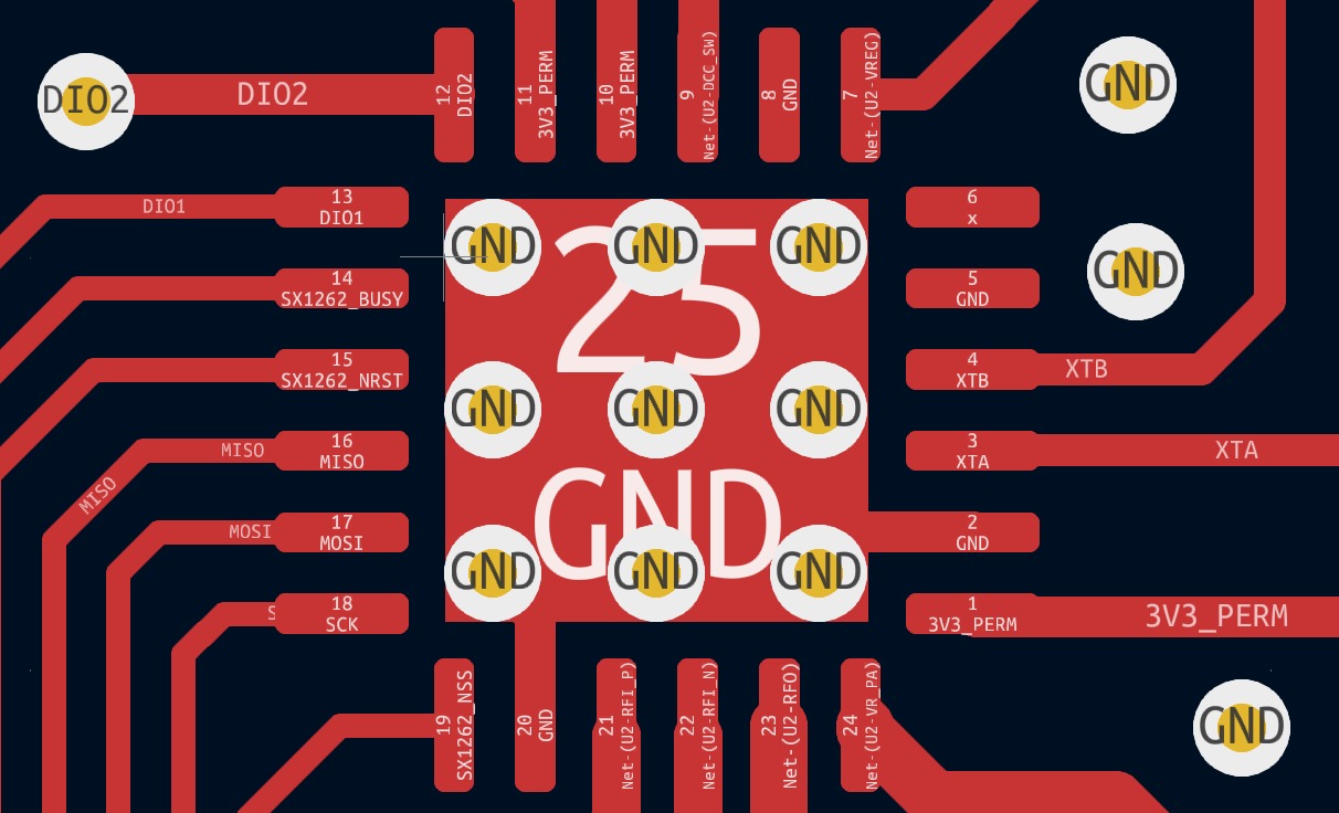
A table of the function and ID of each PIN of the transciever is provided next:
| Pin Number | Pin Name | Type (I = Input, O = Output) | Description |
|---|---|---|---|
| 0 | GND | - | Exposed Ground pad |
| 1 | VDD_IN | I | Input voltage for power amplifier regulator, connected to pin 10 |
| 2 | GND | - | Ground |
| 3 | XTA | - | Crystal oscillator connection, can be used to input external reference clock |
| 4 | XTB | - | Crystal oscillator connection |
| 5 | GND | - | Ground |
| 6 | DIO3 | I/O | Multi-purpose digital I/O - external TCXO supply voltage (NOT USED) |
| 7 | VREG | O | Regulated output voltage from the internal regulator DC-DC |
| 8 | GND | - | Ground |
| 9 | DCC_SW | O | DC-DC Switcher Output |
| 10 | VBAT | I | Supply for the RFIC |
| 11 | VBAT_IO | I | Supply for the Digital I/O interface pins (except DIO3) |
| 12 | DIO2 | O | RF Switch control |
| 13 | DIO1 | O | Interrupt Output to the MCU |
| 14 | BUSY | O | Busy indicator |
| 15 | NRESET | I | Reset signal, active low |
| 16 | MISO | O | SPI slave output |
| 17 | MOSI | I | SPI slave input |
| 18 | SCK | I | SPI clock |
| 19 | NSS | I | SPI Slave Select |
| 20 | GND | - | Ground |
| 21 | RFI_P | I | RF receiver input |
| 22 | RFI_N | I | RF receiver input |
| 23 | RFO | O | RF transmitter output ( high power PA) |
| 24 | VR_PA | - | Regulated power amplifier supply |
Table 1: SX1262 PIN Layout and description
Physically those PINs relate to the following layout in the SX1262:

Figure 3: PIN Layout from the SX1262 top view
The trimming capacitors on the clock may not be connected depending on the clock selection, if it is to be changed. As a matter of fact the transciever offers the possibility of configuring the capacitance of internal capacitors to perform the same task as this ones. On current PoCat design they remain not connected.

Figure 4: Crystal Oscillator Schematic
The switch is controlled through the DIO2 (PIN 12) of the SX1262, selecting the RF2 path (transmission line) when the pin rises to high. If it drops, the path selected will then be the RF1 (reception line). It is supplied with 3.3V through the vertical connectors.

Figure 3: Switch Schematic
The rest of the design follows the reference schematic provided by Semtech on the SX1262 for usual applications with some changes to optimize space and provide testing capabilities, such as the inclussion of a test probe in the transmission line.
The upper part of the connection between the transceiver and the switch transmits the signal generated in the SX1262 (RFO line), then it is amplified (VR PA line) and the harmonics of second and higher order are filtered. The bottom lines are the ones that take the signal received from the switch to the transceiver. As the transceiver needs a balanced signal and the switch provides an unbalanced one, a balun is added in between to do the unbalanced-balanced conversion. One last important aspect is that all the circuits that connect the main components (transceiver-switch-connector) are matched to 50 Ω.

The COMMS PCB must support the schematic presented before with a design that minimized losses and interferences. Its tasks correspond to those stablished in the functional description of the system, mainly providing TT&C (Telemetry Tracking an Command) capabilities, as well as P/L data acquisition.
The COMMS subsystem is encapsulated within the OBC-COMMS PCB, sharing space in the same board. In this section the COMMS related lines and components will be explained while the OBC ones remain in their section.
It is interfaced, like the other PCB's in the stack, with the rest of the boards through vertical connectors on each side. Despite this the only relevant inter-board connections in the COMMS case are both the ground plane and voltage line as well as the antenna itself. The later is communicated through a coaxial connector, one in this PCB and another in a lateral board where the antenna is soldered or screwed.
The PCB has 4 internal layers distributed as shown in the next figure:

Figure 4: OBC-COMMS PCB Structure
An explanation of the layer distribution is provided next:

Figure 4: OBC-COMMS PCB With colored blocks
The power circuit uses the following components:
These two capacitors reduce noise to the input voltage of the transciver and avoid undesired voltage peaks.
| Temp. coeff. or Cap. Change | Temp. Range | Ref. Temp. | Rated Voltage | Capacitance | Capacitance Tolerance | Operating Temp. Range | Mounting Method |
|---|---|---|---|---|---|---|---|
| -15 to 15 % | -55 to 85°C | 25°C | DC 25V | 0.1uF | +/-10% | -55 to 125°C | Flow, Reflow |
This capacitor also avoids coupling from high frecuencies to perturbate the voltage input.
| Temp. coeff. or Cap. Change | Temp. Range | Ref. Temp. | Rated Voltage | Capacitance | Capacitance Tolerance | Operating Temp. Range | Mounting Method |
|---|---|---|---|---|---|---|---|
| -15 to 15 % | -55 to 125°C | 25°C | DC 10V | 1uF | +/-10% | -55 to 85°C | Flow, Reflow |
This capacitor is a part required for the DC-DC Configuration of the transciever.
| Temp. coeff. or Cap. Change | Temp. Range | Ref. Temp. | Rated Voltage | Capacitance | Capacitance Tolerance | Operating Temp. Range | Mounting Method |
|---|---|---|---|---|---|---|---|
| -15 to 15 % | -55 to 125°C | 25°C | DC 35V | 0.47uF | +/-10% | -55 to 125°C | Flow, Reflow |
This inductor is a part required for the DC-DC Configuration of the transciever.
| Inductance (µH) | Tolerance | Typ. DC Resistance (Ω) | Max. DC Resistance (Ω) | Self Resonant Frequency (MHz min.) | Rated Current (mA) (Ind Change.) | Rated Current (mA) (Temp Change.) |
|---|---|---|---|---|---|---|
| 15 | ±20% | 0.95 | 1.235 | 24 | 140 | 250 |
The oscillator block is comprised by the oscillator itself as well as two decoupling capacitors (C27/C28). As of most current design this capacitors are not connected due to the use of the provided internal capacitors in the SX1262.
No relevant components are to be explained of the transciever as they are comprised in other parts. The transciver datasheet is attached here DS SX1262.
The impedance is matched considering a 50Ω load in each side of the line. The values are selected following the reference design provided by Semtech as seen on page 27 of the following document: RT/TX Values
| Inductance (nH) | Tolerance | Max. DC Resistance (Ω) | Self Resonant Frequency (gHz min.) | Rated Current (mA) (Ind Change.) |
|---|---|---|---|---|
| 15 | ±3% | 0.16 | 5.0 | 450 |
| Capacitance | Voltage Rating | Tolerance | Temperature Coefficient | Minimum Operating Temperature | Maximum Operating Temperature |
|---|---|---|---|---|---|
| 1.8 pF | 200 V | 0.1 pF | 0 PPM / C, 30 PPM / C | -55 C | +125 C |
| Capacitance | Voltage Rating | Tolerance | Temperature Coefficient | Minimum Operating Temperature | Maximum Operating Temperature |
|---|---|---|---|---|---|
| 2.4 pF | 200 V | 0.1 pF | 0 PPM / C, 30 PPM / C | -55 C | +125 C |
The transmission line values are also selected following the reference design RT/TX Values and the selected components are the following:
| RefDes | Package | Value | Qty | Description | Manufacturer Code |
|---|---|---|---|---|---|
| C1 | 0402 | 47nF | 1 | Multilayer ceramic capacitors X7R ±10%, 16V | GRM155R71C473KA01J |
| C2 | 0402 | 47pF | 1 | Multilayer ceramic capacitors C0G ±5%, 50V | GJM1555C1H470JB01J |
| C4 | 0402 | 3.3pF | 1 | Silicon RF Capacitor 200V 3.3pF ±0.1pF | 600L3R3BT200T |
| C5 | 0402 | 5.6pF | 1 | Multilayer ceramic capacitors C0G ±0.25pF, 50V | GRM1555C1H5R6CA01D |
| C6 | 0402 | 39pF | 1 | Multilayer ceramic capacitors C0G ±5%, 50V | GJM1555C1H390FB01D |
| C7 | 0402 | 2.2pF | 1 | Silicon RF Capacitor 200V 2.2pF ±0.1pF | 600L2R2BT200T |
| L1 | 0402 | 47nH | 1 | Wirewound Inductor ±2% | 0402DC-47NXGRW |
| L3 | 0402 | 2.5nH | 1 | Wirewound Inductor ±0.2nH | LQW15AN2N5C00D |
| L4 | 0402 | 4.7nH | 1 | Wirewound Inductor ±2nH | 0402DC-4N7XGRW |
The antenna filtering values are also provided on RT/TX Values and the selected components are the following ones:
| RefDes | Package | Value | Qty | Description | Manufacturer Code |
|---|---|---|---|---|---|
| C8 | 0402 | 39pF | 1 | Multilayer Ceramic Capacitors C0G ±5%, 50V | GJM1555C1H390FB01D |
| C9 | 0402 | 3.3pF | 1 | Silicon RF Capacitor 200V 3.3pF ±0.1pF | 600L3R3BT200T |
| C10 | 0402 | 3.3pF | 1 | Silicon RF Capacitor 200V 3.3pF ±0.1pF | 600L3R3BT200T |
| L5 | 0402 | 9.1nH | 1 | Wirewound Inductor ±2% | LQW15AN9N1G8ZD |
Here are some desing considerations taken into account when designing the COMMS side of the PCB, but take into account that the main priorities in the design are to ensure both the fitting of the components as well as their full functionallity in accord to the requirements. After those conditions are met importance is given to basic good practice design guidelines such as:
Component Placement: Critical components, including inductors (e.g., L6) and capacitors (e.g., C12, C11) in the RF signal chain, are placed close to one another to minimize parasitic effects.
Matching Network and Filter: The components along the RX and TX paths are positioned near the IC and connected through short traces.
RF Trace Layout: The RX and TX paths (marked with pink and green arrows) are straight and avoid sharp angles, improving RF signal integrity.
Power Filtering: The use of capacitors and inductors near power inputs and close to ICs ensures that high-frequency noise is filtered out. The capacitors are also placed close to ground to improve noise reduction.
Oscillator Placement: The oscillator is located away from the RF signal paths, which reduces the risk of interference from clock harmonics.
EMC and Via Stitching: The board includes via stitching in the corners and around the perimeter, and the layout keeps return paths close to the corresponding signal paths.
Overall good practices and PCB Guidelines are also provided by the manufacturer in the following document: PCB Guidelines
The communication methods employed by other satellites bear a strong resemblance to ours, albeit with some differing aspects such as signal frequency and power. For instance, in the case of Alba Orbital PocketQubes, the transceiver operated within the 145/435 MHz range from the radio amateur band. Additionally, other types of satellites like CubeSats have the flexibility to incorporate power amplifiers, enhancing signal strength, an option not feasible for PocketQubes due to their restricted size and power limitations. Consequently, the power and bandwidth capabilities of signals in other satellites enable them to achieve higher data rates and transmit data of superior quality.
In the general structure, the fundamental principle remains consistent: a transceiver is responsible for both transmitting and receiving signals. These signals undergo filtration in the transmission and reception chains, modulation and demodulation before being distributed to their respective destinations.
# Software DesignCOMMS Software is integrated within the MCU and designed as a state machine that transitions mainly due to the recival and transmission events. Most of the relevant code is encapsulated within the COMMS Task, in terms of FreeRTOS structure. The software is then responsible for the proper handling of each telecommand received as well as beacon transmission among other functinalities such as:
In terms of telemetry, in a nominal state:
Do note that as the PQ enters either SUNSAFE or SURVIVAL TT&C becomes heavily restricted in favour of mission preservation. In SUNSAFE the only telemetry available will be the periodically transmitted beacon, dedicating all other task time to active listening.
In SURVIVAL the telemetry capabilities of the satellite are completely deactivated until a change of state occurs, only actively listening for telecommand for a set period of time. In case of TC reception, the most critical beacon data is sent in response in order to assess the spacecraft state.
As of current design the COMMS State Machine is composed by a total of five states. The first state corresponds to STARTUP, where the transciever is reset and initialized. After initialization the radio will start alternating between its sleep mode and CAD or reception mode (tbd), all within the SLEEP state.
In case of being in CAD Mode and having detected activity the machine will enter the RX state and actively listen for a specified value of time. In case of surpassing said value with no packets received the machine will go back to SLEEP, and so will do in case of receiving a packet not sent by the GS. An RX Error during this process also returns the machine to SLEEP.
In case of not being in CAD Mode in the SLEEP state a successful packet receival will send the machine to the RX state, so as to process the TLC. This will also happen when as TLC is received in the RX state when CAD Mode in set on.
The successful receival of a TLC will enter us into the TX state. Here either p/l data will be sent, awaiting for ACK's in this case (ARQ), returning to RX (after TxDone), or telemetry (!ARQ), sending the machine to the SLEEP state (after TxDone).
As the time to send a beacon arrives the machine is to be notified by the OBC and enter the TX state to transmit it.
During the RX state it might occur that a TLC is received indicating transciever parameters are to be changed. This will send the machine to the STDBY (Standby) state, as it is required to do so. In case of having to reset the SX1262 this state will also be present as an intermediary before STARTUP.
The STARTUP state can also be forced to enter through a OBC Notification to the task itself. The state machine also checks for IRQ and OBC notifications in every iteration, independently of the current state.

Figure 1: COMMS State Machine
As of current design both uplink and downlink telecomunications are subject to a similar EDAC procedure. As is discussed before different coding rates might be chosen in order to trade-off security for speed and vice-versa, leaving an open space for different options.
LoRa already puts in use it's own convolutional coding in every transmission, so no further layer is added. On the other hand interleaving is used in order to minimize the burst errors expected to occur due to atmospheric scintillation and other variables. This means that messages are to be manually encoded and decoded at both nodes of communication.
When it comes to verifying transactions ACK's are an essential part of the game. All telecommands that do not induce the direct transmission of data to the GS have been atached the sending of an ACK as a part of their processing. Thankfully in many cases the direct purpose of a TLC is to retrieve data from the PQ, meaning that receiving said data is enough of an ACK.
Extracting payload data gets more tricky. As of current design a Stop-And-Wait (Sliding Window of step w)? ARQ is implemented in order to ensure zero loss of data in case of link loss during transmission. This is done through the request of a specified number of packets (window). In case of successfully receiving all the expected packets the GS might send a TLC (with an incorpored ACK) requesting the next batch or data or indicating a new operation.
The aforementioned case can be found when the PQ has to send multiple packets in a single operation to the GS. The opposite might occur, as it does when sending the TLE to the PQ. The TLE TLC consists of multiple packets. The approach taken is to send the full TLE TLC and await for the receival of an ACK. Should a NACK arrive all packets are to be sent again, as the PQ will expect the GS to do so.
Further visual and specific information is found on the next sections about this topic.
All data, both in uplink and downlink, is interleaved in order to minimize the effects of burst errors. Further encoding is done outside our scope by the LoRa modules, with a set coding rate (CR) of 4/5. CRC is also provided by the LoRa modules. A simple diagram is provided next:

Figure 2: Encoding and Decoding Schemes
Note that the data is not only further encoded and decoded but also modulated and demodulated by the transcieverswithout any other device or software processing.
Interleaving is an encoding technique which is based on the reordering of bytes aiming to prevent burst errors. It is of great relevance when the information contained in a byte also provides information about it's neighbour, such as in the case of payload data. An example of how interleaving works will is shown below.
First of all, the data before the interleaving process is divided into 4 codewords, and each one is presented in a different colour.
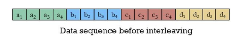
Figure 3: Interleaving example step 1: Data without interleaving.
The second step is to organize the codewords in columns forming a 4x4 matrix.
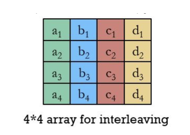
Figure 4: Interleaving example step 2: Data in a square array.
And finally, the data is retrieved row by row from the 4x4 matrix.

Figure 5: Interleaving example step 3: Data after interleaving.
This way, if there is a burst error such as the one shown in the previous picture (the white bytes), instead of affecting a whole codeword, it is spread through the data sequence (as seen in the figure below), thus errors are isolated and easier to correct.
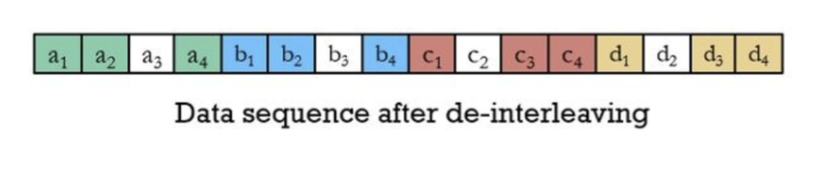
Figure 6: Interleaving example step 4: Data after de-interleaving.
This will only work if the packet lenght is a square number, therefore padding is be added in cases where this condition is not met.
This section is oudated in respect to current design. New telecommands have been designed in order to facilitate debugging, testing and providing a more thorough control of the spacecraft. These can be found on the Operations book. Reed Salomon encoding has also been dropped out. All the aforementioned changes will be reflected on future versions of the Wiki and software.
Telecommands are the mesages or instructions send by the Ground Station to the satelite that indicate it to perform a specified task. The opposite data, the one sent by the spacecraft to the GS, receives the name of telemetry.
This telecommand orders the PocketQube to do a soft reset. This is required in case of software malfunctioning when the satellite is experiencing unexpected behaviour.
The structure of this telecommand is:
Then, this content is interleaved and the output is transmitted.

This telecommand, as its own name implies, requests the exit from a state. The state desired to exit is sent as a parameter inside the telecommand.
The structure of this telecommand is:
Then, this content is interleaved and the output is transmitted.

In fact, a Two Line Element has 3 lines. The first one is for the satellite name, thus, in this case, it can be neglected. Then, two lines of 69 Bytes each contain the orbital elements from which the orbit of the satellite can be computed. This telecommand is used to update the orbit information in the PocketQube needed to propagate the orbit.
As commented previously, the maximum payload size allowed is 48 bytes (taking into account the multiples of 16). Thus, 4 packets will be needed to send the two lines of 69 bytes from the TLE because, from the 48 bytes, only 34 are reserved for data.
Two designs have been implemented given the fact that the last packet only transports 18 bytes of the TLE. The first 3 packets will follow this structure:
3 bytes of header formed by 2 bytes of PIN and 1 byte of telecommand ID,
40 bytes of the TLE orbital elements,
4 bytes of a Unix time timestamp,
1 end byte equivalent to 0xFF. Regarding the last packet, it will have the following structure:
3 bytes of header formed by 2 bytes of PIN and 1 byte of telecommand ID,
18 bytes of the TLE orbital elements,
4 bytes of a Unix time timestamp,
1 end byte equivalent to 0xFF.
22 bytes of '0''s. Each packet will also be interleaved before being sent.

This telecommand orders the PocketQube to send the payload data.
The structure of this telecommand is:

This telecommand orders the PocketQube to send the telemetry data so it does not have to wait for the beacon to be transmitted.
The structure of this telecommand is:

In the payload data transmission, since lots of packets are sent in a row, to avoid the interruption of the transmission, only a packet will be sent at the end with the information of the packets that were received and the ones that were not.
The structure of this packet depends on the number of received packets:
Then, this content is interleaved and the output is transmitted. In this packet structure, padding might be added if the number of ACK bytes is not enough to construct a packet with a length multiple of 2^#.

This packet sends the whole ADCS parameters needed to calibrate and then, when the PocketQube receives it, the calibration is carried out.
This structure will be changed in the near future.


The UPLINK CONFIG telecommand sends the desired PocketQube configuration to the satellite and once it is received, the parameters are compared to the ones stored in the PocketQube. If the parameters do not match, the values are updated.
The structure of the telecommand is:
3 bytes of header formed by 2 bytes of PIN and 1 byte of telecommand ID,
18 bytes of configuration data,
4 bytes of a Unix time timestamp,
1 end byte equivalent to 0xFF, and
11 bytes of padding to reach the next multiple of 2^#, which is 32 bytes. The configuration data can be broken into:
4 bytes of Unix time used for synchronization, - 4 bytes of communication parameters such as spreading factor, coding rate, frequency etc., - 1 byte for the KP constant (the equilibrium constant), and - 3 bytes for the battery thresholds of the nominal, the low and the critical states (one byte each).
Then, this content is interleaved and the output is transmitted.

This telecommand requests a change of receiving timeout of the PocketQube. This might be useful if the spreading factor is increased which implies slower transmissions.
The structure of this telecommand is:

This telecommand is sent when the payload must be activated either for a photo or for an RFI measurement (depending on the payload of the POCAT). All the characteristics of the photo or measurement along with the payload configuration are specified in the telecommand.
The structure of this telecommand is:
First of all, 6 bytes with information related to the photo (in case the PQ has no camera as payload these bytes are set to 0), which can be broken down into:
4 bytes of Unix time to inform when to take the next payload data acquisition,
1 byte to request a specific compression for the photo, and
1 byte to ask for a specific photo resolution. Followed by 12 bytes for the RFI measurements (in case the PQ has no monitoring receiver as payload these bytes are set to 0) divided into:
Then, this content is interleaved and the output is transmitted.

This telecommand asks the PocketQube to send its configuration packet in order to check if everything is working properly. In case something is not as expected, the UPLINK CONFIG telecommand is sent specifying the desired parameters to modify.
The structure of this telecommand is as follows:
Then, this content is interleaved and the output is transmitted.

The telemetry packet is transmitted when the ground station sends the SEND TELEMETRY telecommand. Moreover, the telemetry is also sent in the beacon packet which is transmitted every minute. Inside this packet is gathered information from different PocketQube subsystems. The global structure is:
3 bytes of header formed by 1 byte of Mission ID, 1 byte for the PocketQube ID and lastly 1 byte for the packet ID (in this case the telemetry ID), - 91bytes for the telemetry data, - 4 bytes of a Unix time timestamp, - 1 end byte equivalent to 0xFF, and - 11 bytes of padding in order to reach 48 bytes and do proper interleaving. The telemetry data can also be broken down into the different subsystem’s data:
4 bytes for the EPS. This subsystem has the following distribution of information: •1 byte to store the electrical power system voltage used
•1 byte to store the electrical power system current used
•1 byte for the battery capacity, and
•1 byte for the subsystem temperature.
3 bytes for the OBC. This subsystem information is broken into:
• 3 bits for the PocketQube state (Init, Nominal, Contingency, Sunsafe, Survival and Waiting),
• 2 bits for the Point of Load,
• 3 bits for the PocketQube state error flags,
• 2 bits for the EPS errors such as CHRG (corresponds to an error during the charging process) or FAULT (this is a generic error),
• 6 bits for the communication protocols errors such as I2C, SPI, UART errors, and
• 1 byte to store the onboard computer temperature.
14 bytes for the ADCS. This other subsystem information can also be divided into:
• 6 bytes for the information on the gyroscope,
• 2 bytes for the magnetometers information,
• 3 bytes to store the sun vector,
• 2 bits for the ADCS mode. There are two possible modes, measuring and actuating,
• 6 bits for the magnetic torquer level, and
• 1 byte for the subsystem temperature.
7 bytes for the PQ temperature: This is not a subsystem, but it is a critical topic that needs to be included in the telemetry. It is also subdivided into:
• 6 bytes for each solar panel (+X, -X, +Y, -Y, +Z, -Z), and
• 1 byte for the battery temperature.
Then, this content is interleaved and the output is transmitted.

The data packets are all sent in a row when the PocketQube receives the SEND DATA telecommand. There will be as many packets as needed in order to transmit the whole payload data.
The telecommand is formed by:
Then, this content is interleaved and the output is transmitted.

The configuration packet is transmitted from the PocketQube to the ground station when the SEND CONFIG telecommand is received. This packet has the same structure as the UPLINK CONFIG telecommand except for the 2 bytes of PIN ID which are replaced by the mission ID and the PQ ID bytes.

The purpose of this section is to conduct a complete test of the COMMS subsystem following the soldering of the board or after completing environmental tests. These tests are essential to ensure that the COMMS subsystem hardware is functioning as intended.
The entire test is outlined in the following diagram:
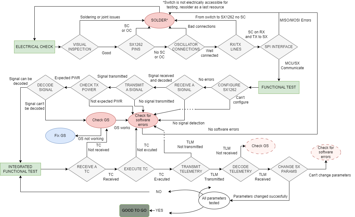
Figure 1: COMMS Development and Verification Plan.
COMMS SDV starts with a visual inspection of the soldered board, in search for easily detectable mistakes and solder issues. The next step is to manually verify the connections on the SX1262 (Transciever) pins, as OC might be common if care is not taken when soldering. The oscillator presents as a moderately hard to solder piece so it is easy and useful to ensure that the lines connecting the crystal to the SX1262 and the planes are properly set-up. A critical piece to verify is the switch, but to do so electrical checks are not easy to perform. Its status will be verified by the transmission and reception operations. RX/TX go all the way from the switch to the transciever, so a simple contituity check suffices to verify the line integrity, Finnally, with the help of the OBC the SPI interface is tested to verify communications.
As communication between the MCU and the SX is ensured it is time to test the basic operations to be performed by the COMMS subsystem, mainly receival and decoding as well as transmission of signals at appropiate power. Several points of failure appear in these steps, mainly software errors and GS errors. It might also occur that the previous electrical check did not completely sort out all isues, creating the need for further hardware inspection.
The final steps are to verify the board and susbsystem is to test several operations to be done by it. Telecommands are to be received, executed and telemetry is to be transmitted and decoded by the GS. Finally it is optimal to test the system with different configurations as parameters might be changed on-the-fly during the mission. If this step is accomplished the board is considered good to go.
The purpose of this section is to conduct an electrical check of the COMMS subsystem following the soldering of the board or after completing environmental tests.
Always ensure you're grounded to prevent static electricity from damaging the electronic components on the board.
| Requirement ID | Description |
|---|---|
| COMMS-EC-001 | All components and connections shall be visually inspected to ensure proper soldering, absence of damage, and correct placement of wires. |
| COMMS-EC-002 | Each SX1262 pin shall be securely connected to its corresponding circuit point, with no shorts or floating pins present. |
| COMMS-EC-003 | The oscillator shall be checked to ensure its connections are properly soldered and it is operating at the specified frequency. |
| COMMS-EC-004 | The receive (RX) and transmit (TX) lines shall be inspected to confirm they are properly wired, with no interference or signal degradation. |
| COMMS-EC-005 | The SPI interface shall be validated to ensure correct wiring and successful communication between the microcontroller and the SX1262. |
| COMMS-EC-006 | All solder joints shall be inspected to verify they are strong and free from defects, with any weak joints re-soldered as needed. |
| Description | Pass Criteria | Fail Criteria |
|---|---|---|
| Visual inspection of components, soldering, and wire placement. | Components and lines are securely soldered and correctly positioned, with no visible cracks in the soldering or components, melted parts, or misaligned elements. | Improper soldering, damage, or incorrect placement. |
| Secure connections for SX1262 pins, with no shorts or floating pins. | All pins are securely connected, no shorts or floating pins. | Pins are loose, shorted, or floating. |
| Check oscillator connections and frequency. | Oscillator is correctly soldered and operates at the right frequency. | Faulty connections or incorrect frequency. |
| Inspect RX and TX lines for proper line and signal quality. | RX and TX lines are correctly connected with no signal issues. | No signal, interference, or signal degradation are observed. |
| Validate SPI interfaces and communication. | SPI is correctly connected and communication is successful. | Incorrect connection or communication failure. |
| Inspect solder joints for strength and defects. | Solder joints are strong and defect-free. | Weak or defective joints require re-soldering. |
| Step - ID | Description |
| EC-TEST-01 | Using a microscope or equivalent tool, perform a visual inspection of the OBC-COMMS board to check for damaged components or traces, as well as displaced or missing components, and cracks in the solder joints. If any damaged elements are identified, replace them or conduct additional tests to assess their functionality. |
| EC-TEST-02 | Using a multimeter, verify that all pins of the transceiver (SX1262) are properly soldered, correctly positioned, and free of any unwanted short circuits or open circuits. |
| EC-TEST-03 | Repeat the previous step for the oscillator connections. |
| EC-TEST-04 | Use a multimeter to verify that the entire RX-TX chain is free of any unwanted shorts or open circuits. Pay extra attention to the switch, as it has 6 pins in a confined space. |
| EC-TEST-05 | After inspecting the COMMS subsystem, the final step is to verify the connections between the transceiver and the On-Board Computer. Specifically, use a multimeter to ensure that all SPI connections are secure. The pins to check include SX1262_NSS, SCK, MOSI, MISO, SX1262_NRST, and SX1262_BUSY. |
If the electrical check is successful, proceed to the functional testing of the COMMS subsystem. Keep in mind that in some cases, such as after a vibration test, the board may sustain subtle damage, so proceed with extra caution!
The purpose of the functional test is to achieve a successful transmission using the OBC-COMMS board.
| Requirement ID | Description |
|---|---|
| COMMS-FT-001 | The SX1262 configuration parameters (SF=11, CR=4/5), including frequency (868 MHz), modulation (LoRa), and power settings, shall be correctly set for the test. |
| COMMS-FT-002 | The device shall transmit a signal that is detectable at the intended range (frequency and power) with minimal signal degradation. |
| COMMS-FT-003 | The transmission power level shall be verified to meet specified limits and be consistent with expected output. |
| COMMS-FT-004 | The device shall successfully receive signals without interference or loss of quality during the test. |
| COMMS-FT-005 | The device shall decode incoming signals accurately without errors during the functional test. |
| Description | Pass Criteria | Fail Criteria |
|---|---|---|
| The SX1262 configuration parameters (SF=11, CR=4/5), including frequency (868 MHz), modulation (LoRa), and power settings, shall be correctly set for the test. | Parameters are set correctly as per specification (SF=11, CR=4/5, frequency=868 MHz, modulation=LoRa, power at specified level). | Parameters are incorrectly set, or any configuration setting is missing or erroneous. |
| The device shall transmit a signal that is detectable at the intended range (frequency and power) with minimal signal degradation. | Signal is transmitted and detected within the specified range, with acceptable signal quality and minimal degradation. | Signal is not detectable, outside the intended range, or shows significant degradation. |
| The transmission power level shall be verified to meet specified limits and be consistent with expected output. | Transmission power meets specified limits and aligns with expected power output. | Transmission power is inconsistent with expected output. |
| The device shall successfully receive signals without interference or loss of quality during the test. | Signals are received with clarity, no interference, and within acceptable quality limits. | Signal reception is poor, shows interference, or lacks quality. |
| The device shall decode incoming signals accurately without errors during the functional test. | Signals are decoded correctly without errors, and data integrity is maintained. | Decoding fails, produces errors, or results in data integrity loss. |
| Step - ID | Description |
| FT-TEST-01 | Connect the OBC-COMMS board to a computer using the ST-LINK v2, concretely connect the RST, 3.3V, GND, SWCLK and SWDIO pins to the board. |
| FT-TEST-02 | After connecting the board to the laptop using an ST-LINK, upload the code to the board. You may want to add breakpoints to examine each step of the transmission process in detail. |
| FT-TEST-03 | After flashing the code, use a Spectrum Analyzer to visualize the transmission’s power, frequency, and other parameters more effectively. |
| FT-TEST-04 | After verifying the basic parameters of the transmitted signal, proceed to test the Ground Station's ability to correctly decode the signal. Configure the a TinyGS for a reception test of the transmitted signal. |
| FT-TEST-05 | Transmit a signal, ideally containing user-generated telemetry data, and verify that the Ground Station has accurately received and decoded all transmitted information. This test can be repeated with different types of data, such as payload data. |
| Requirement ID | Description |
|---|---|
| COMMS-IFT-001 | The system can receive telecommands, including those consisting of multiple packets. |
| COMMS-IFT-002 | The COMMS system successfully executes telecommands upon correct reception and generates a response if the telecommand requires it. |
| COMMS-IFT-003 | Once a response is generated, the COMMS subsystem transmits it accurately at the specified frequency (868 MHz), output power (22 dBm), spreading factor (11), and coding rate (4/5). Same requirement applies for the telemetry which is sent periodically by the spacecraft. |
| COMMS-IFT-004 | The received telemetry and/or telecommand is correctly decoded by the Ground Station. |
| COMMS-IFT-005 | All parameters updated via telecommand on the PocketQube are accurately applied, including configuration adjustments and payload activation settings. |
| Description | Pass Criteria | Fail Criteria |
|---|---|---|
| x | x | x |
| x | x | x |
| x | x | x |
| x | x | x |
| Step - ID | Description |
| x | x |
| x | x |
| x | x |
| x | x |
| x | x |
The aim of this document is to clearly explain the tests performed during the delevolpment of the subsystem.
This document is based on current but also previous versions both of hardware and software and as such be followed with care.
Antenna impedance matching is a crucial aspect in the design and operation of radio frequency systems. Impedance matching involves adjusting the impedance of the antenna to match the impedance of the transmission line or the RF source to which it is connected. The objective of the test will be to determine the length of the quarter wavelength monopole antenna for the satellite.
| Requirement ID | Description |
|---|---|
| AMT - 01 | The antenna should exhibit impedance values closely matching the specified target impedance across the defined frequency range (868 MHz). |
| AMT - 02 | Return loss values should be high, indicating a low amount of power reflected back towards the source and efficient power transfer. |
| AMT - 03 | The antenna should demonstrate acceptable impedance matching and performance across the specified bandwidth(125kHz). |
| Parameter | Pass Criteria | Fail Criteria |
|---|---|---|
| Return Loss | Return Loss < -10 dB (lower values are better) | Return Loss > -10 dB (indicating poor matching) |
| Standing Wave Ratio (SWR) | SWR < 2:1 (lower values are better) | SWR > 2:1 (indicating poor impedance matching) |
| Impedance Matching | Impedance matched to system requirements | Significant deviation from desired impedance |
| Radiation Pattern (optional) | Symmetrical and aligned with specifications | Irregular pattern, beam tilting, or distortions |
| Step - ID | Description |
| AMT\_S-01 | Prepare the Testing Environment:
|
| AMT\_S-02 | Calibrate the Vector Network Analyzer:
|
| AMT\_S-03 | Connect the Antenna:
|
| AMT\_S-04 | Measure the Antenna Impedance:
|
| AMT\_S-05 | Analyze Measurement Results:
|
| AMT\_S-06 | Optimize and Fine-Tune (if needed):
|
| AMT\_S-07 | Save and Store Data:
|
The test was conducted in the autumn of 2022, and the outcomes are as follows:

As can be seen in the figure above, the final antenna had RL(dB) = -10 for the operating frequency. Moreover, the bandwidth of the antenna is approximately 15 MHz.
The result obtained from this test, however, is quite surprising: the antenna length must be 3.5 cm, which is much lower than what was theoretically calculated (8.64 cm). The reason behind this result could be the non-ideal ground plane of the monopole.
Obtained antenna lenght is 3.5 cm, lower than what was theoretically calculated (8.64 cm).
Test should be redone with the final version of the PocketQube.
The objective of this test is to validate the correct operations of the COMMS layout in the PocketQube with the OBC&COMMS board.
| Requirement ID | Description |
|---|---|
| OCBT - 01 | Be able to see MISO, MOSI, SCK, SX1262-NSS, SX1262-NRST and SX1262-BUSY signals. |
| OCBT - 02 | Be able to decodify MISO, MOSI and SCK |
| OCBT - 03 | MISO, MOSI and SCK decodification must match expected results of the datasheet. |
OBC&COMMS with only used pinouts:

If we zoom into the COMMS chip we get the following:
We'll measure the following pins: MISO, MOSI, SCK, SX1262_NSS. These are the only ones available for comparison with the expected values outlined in the datasheet.


We will connect the ST-LINK v2 to a PC for flashing code. The SWDIO, SWCLK, and 3.3V ports of the ST-LINK v2 will link to pull-up resistors shown in the following image before connecting them to their respective pins. Meanwhile, the other ports (GND and RESET) will be directly linked to the board.

To verify the functionality of the COMMS chip, we'll compare the obtained results with the expected specifications outlined in the SX1262IMLTRT datasheet.
The test will be deemed successful if our obtained results align with those specified in the datasheet. If they don't correspond, the test will be considered unsuccessful.
| Step ID | Description | Pass/Fail Criteria | Actual | Passed(Y or N) |
| CS - 01 | Prepare the setup explained in the previous step | Flashing must be successful, a "successful message" must appear | We encountered a lot of issues when flashing due to poor connections, after many attemps we successfully flashed | Sometimes, had to repeat multiple times until it worked |
| CS - 02 | Flash code, we used the main program (Project>>Build All + Run>>Debug As>>1STM32C...) | |||
| CS - 03 | Using Saleae, check all pins of the SX1262 chip, especially MISO, MOSI, SCK and SX1262-NSS | Just after flashing we must see signals in all these pins | Only MISO had a visible signal, the others had not | No, no signal was spotted in MOSI, SCK and SX1262-NSS. |
| CS - 04 | Once we have simultaniously captured MISO, MOSI and SCK, decodify the signal | Comparing with the SX1262 datasheet, the decodification must be the one we expected | Since we only obtained the MISO signal, it has been impossible for us to decode | No |
We encountered several issues while working on the project. Firstly, we faced weak connections between the board and the computer for CS-01 and CS-02, which resulted in several days of troubleshooting. We had to solder connectors to establish a stable connection, but the board remained fragile, and we couldn’t touch it much.
Moving on to CS-03, we encountered three major issues. The first issue was with the tool we used for decodification. We needed three ports to capture all three signals (MISO, MOSI, and SCK) simultaneously, so we had to switch from PicoScope to a Saleae device. The second issue was the small size of the chip and connections, which made it extremely difficult (if not impossible) to capture all signals simultaneously. We recommend adding testing pins to the board in future versions. Finally, the third issue was with the decodification process itself. We could only observe MISO, SX1262_NRST, SX1262_NSS, XTA, and XTB signals. Since we also needed MOSI and SCK signals to decode the signal, we were unable to do so. We also checked the power pins going to the SX1262 and found no issues.
As for CS-04, we were unable to compare it with the datasheet since we couldn’t decode it.
During the project, we faced several issues. As previously mentioned, we encountered anomalies during the test, including fragile connections, small pins on the chip that made it difficult to check all signals simultaneously, and no signal for MOSI and SCK. Unfortunately, we were unable to decode the signal.
As the COMMS subsystem relies heavily on this crucial test, essential for communication testing, we've opted to temporarily skip it. Instead, we will use a spectrum analyzer to verify if the chip is transmitting signals. If successful, it confirms effective communication between the OBC and COMMS chips. However, if no signals are detected, the issue may lie in the connections/design of the board.
Due to the outcomes of the OBC-COMMS board test, an alternative method is required to validate ongoing communication between the OBC and COMMS chips. To achieve this, we plan to establish communication between a TinyGS and the OBC-COMMS board, effectively simulating the connection between a ground station and our satellite. Furthermore, attenuations will be introduced later in the process to mimic the conditions present in space.
| Requirement ID | Description |
|---|---|
| RXTX - 01 | Be able to transmit using a TinyGS. |
| RXTX - 02 | Be able to receive the transmitted data using the SX1262. |
| RXTX - 03 | Possess the capability to respond to specific telecommands by transmitting a reply. |
| RXTX - 04 | Have the capability to initiate communication between the TinyGS and the OBC-COMMS while incorporating attenuations. |
| RXTX - 05 | Possess the capability to process telecommands and provide responses while incorporating attenuations. |


For the initial and fundamental phase of our test, the setup is as follows:
One computer will be connected to a TinyGS, while the other computer will have a Nucleo+LoRa module connected to it. This configuration allows us to verify the transmission capability of the TinyGS and the responsiveness of the board (initially represented by an STM32 Nucleo + LoRa module).
The setup for the STM32 Nucleo + LoRa module is the following:

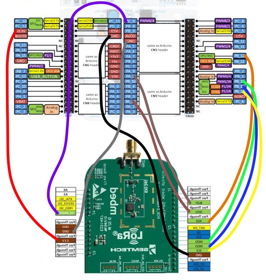
After successfully testing this setup, the next configuration is as follows:
Instead of the Nucleo+LoRa, we will integrate the OBC-COMMS board from the OBC-COMMS board test.
As we advance in the testing process, we will introduce a variable attenuator in either reception or transmission.
Throughout the experiment, a spectrum analyzer will be employed to detect the signals transmitted, while the TinyGS console will be utilized to monitor both sent and received data.
The experiment will be deemed successful if the specified requirements are fulfilled, signifying our ability to transmit effectively using the TinyGS, and the OBC-COMMS board responds as anticipated, both in the presence and absence of attenuation.
The initial phase of this test involves configuring and preparing a TinyGS station. Since a similar station has been utilized in previous tests, please refer to the instructions provided in the "ᴾᵒCat Testing >> ᴾᵒCat SSVs >> COMMS Software SSV" section for guidance.
Once our TinyGS is configured we can test its transmission capabilities by sending one of the telecommands shown in the TinyGS console. For checking the correct transmission we will used a spectrum analyser. 
If encountering transmission difficulties, we can attempt communication between two TinyGS units. This approach allows us to showcase the capability of our TinyGS in both sending and receiving data. The necessary steps involve configuring a second TinyGS (just like we did with the first one) and issuing a telecommand, with the option to utilize the "p" command for sending a test packet.
Upon confirming the proper functionality of the TinyGS, the next step is to connect the STM32 Nucleo + LoRa module to the computer. Subsequently, we will flash our code into it to activate the reception mode of the SX1262 (LoRa module). Finally, we will initiate transmission using the TinyGS and observe if the STM32+LoRa module responds. For this test we will only take into account the "FLASH" and "COMMS" tasks.
After confirming the correct functionality of the code on the STM32 Nucleo + LoRa module, we can proceed to the next stage of utilizing the board. If the preceding tests yield success, but this phase encounters issues, we can confidently conclude that the issue lies in the hardware rather than the software, thereby narrowing down the potential sources of errors.
If all the preceding steps are successful, the next phase involves experimenting with attenuators to simulate the conditions our system will encounter in space. Common attenuators and a variable attenuator will be employed for this purpose. The objective of this step is to assess the feasibility of transmission under various influencing factors such as distance, speed, angle of the antennas, and other relevant parameters.
The configuration of the TinyGS for transmission and reception at 868MHz was completed successfully.
The TinyGS exhibits the ability to both transmit and receive data, as exemplified by the successful demonstration using two TinyGS units. In the event of possessing only one TinyGS, we can showcase the effective operation of the ground station by employing a spectrum analyzer and receiving signals from satellites that are using the TinyGS network.
Upon flashing our code into the Nucleo and transmitting diverse telecommands with TinyGS, we discovered that the LoRa module failed to transmit responses to the telecommands as expected. Following a thorough and extensive investigation, we identified the root cause of the issue: during reception, the reception buffer requires slightly more time before decoding to effectively process the incoming packets. To address this issue, we implemented a solution by incorporating a small delay. Following this adjustment, we have successfully achieved the reception and response to telecommands sent by TinyGS, as demonstrated in here:
We will commence with telecommands that do not necessitate a response from the PocketQube. To verify proper functionality, we will insert breakpoints within each of these states for testing.


Subsequently, we will perform tests on all telecommands that necessitate a response from the satellite. To test these telecommands, we can choose to either insert breakpoints or examine the responses from the TinyGS terminal.


We can affirm that all telecommands have been successfully transmitted by TinyGS, processed by the Nucleo+LoRa, and appropriately answered when required.
Following the success of the previous step, we proceeded to integrate the actual OBC-COMMS board. However, the experiment deviated from the plan due to several issues:
While we initially anticipated hardware-related problems, a careful examination of variable values (such as the COMMS state or PacketReceived) suggests a potential issue with the OBC and task management rather than the hardware.
To address these issues, several actions were taken:
UPDATE: Errors were detected on the OBC-COMMS board
1) Mirroring error in one of the OBC crystal oscillator:
The error has already been corrected in the newest OBC-COMMS PCB design. The clock was removed from the board for this test as

2) Issue with the transceiver clock capacitors. Both transceiver crystal oscillators were removed as per the transceiver datasheet: "The SX1261/2 does not require the user to set external foot capacitors on the XTAL supplying the 32 MHz clock. Indeed, the device is fitted with internal programmable capacitors connected independently to the pins XTA and XTB of the device. Each capacitor can be set independently, balanced or unbalanced to each other, by 0.47 pF typical steps."
Both capacitors were removed.
After implementing the commented modifications to the board, the testing was resumed:
TBD.
As we've been reviewing the test results, several issues were encountered during the process:
During step 3, an issue arose during the reception process, which was successfully resolved by introducing a slight delay. The issue caused the system to "ignore" the sent telecommands.
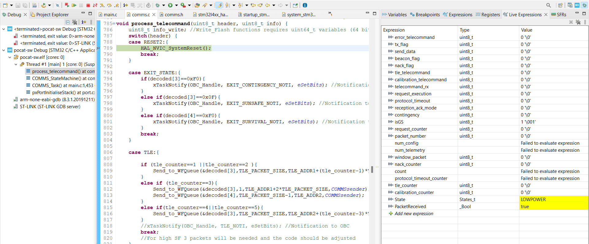
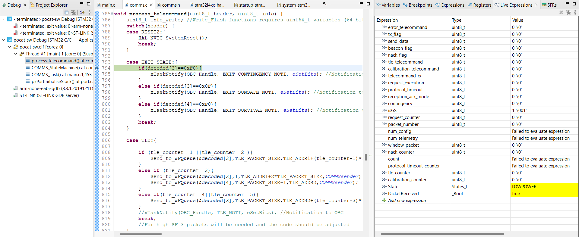
In step 4, the COMMS subsystem persisted in LOWPOWER mode, necessitating the removal of tasks to facilitate the test. This indicates an ongoing challenge with the OBC subsystem task.
Another issue in step 4 involved the reception of numerous packets from unidentified sources. To address this, further solutions are needed, and the possibility of conducting tests within an anechoic chamber is being considered for better-controlled testing conditions
The issue pertaining to OBC task management must be tackled, as it seems to be the primary cause of the anomalies we discussed.
Furthermore, we must also tackle the problem of receiving numerous packets, as it hinders the reception of the genuinely important ones.
At the very least, we can affirm that the COMMS code is functioning correctly, and the OBC-COMMS board, equipped with the quarter-wavelength antenna, is capable of successfully receiving packets.
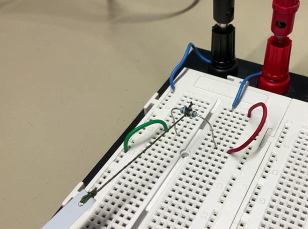
This test aims to evaluate the chosen Dyneema for the antenna deployment. It involves measuring the time taken for the material to melt under atmospheric conditions.


If Dyneema melts within the range of 10 to 15 seconds at 3.3V and 450mA, the test can be deemed successful. However, if it takes longer or fails to melt, the test will be considered unsuccessful.
The knot is connected to the resistor and the power source is connected. We used the weight of the lateral board with the antenna to simulate some pressure.
The knot starts showing signs of degradation as the temperature of the resistor increases.

The knot melts and the pressure provoques the antenna to deploy.

Some calculations:
Power (W) = Voltage (V) * Current (A) = 3.3 * 0.45 = 1.485 W
Energy consumed (J) = Power (W) * Time (s) = 1.485 * 14 = 20.79 J
None. After repeating this test, it was determined that it needed to be redone as the dyneema did not burn, but melted instead.


Possible problems with the EPS. Redo the test.
This experiment will undergo repetition within a vacuum chamber due to the differing thermal properties in such conditions. Dyneema is expected to exhibit a significantly faster melting rate as heat transfer with the absence of air in space is not a factor.
The primary goal of this test is to validate the satellite's antenna deployment. This step is mission-critical as its proper function is pivotal for the transmission and reception of data by the satellite.
This test might (if possible) also test the comunications with the deployed antenna.
| Requirement ID | Description |
|---|---|
| ADTR - 01 | Dyneema must melt in less than 15 seconds in vacUum conditions. |
| ADTR - 02 | The antenna must deploy correctly, meaning that it should remain nearly completely straight after deployment. |
| ADTR - 03 | The spacecraft must be able to communicate with the ground station after antenna deployment |
If the Dyneema melts in under 15 seconds in vacuum conditions and the antenna remains straight post-deployment, we will deem the antenna deployment test successful.
Prior to conducting a test in the vacuum chamber, it is imperative to meticulously examine the feasibility of the test in atmospheric conditions. While the results may vary, the ultimate conclusion remains the same: if the dyneema melts in atmospheric conditions, it will likewise experience the same outcome in vacuum conditions.
To carry out this preliminary test, a PocketQube with, at a minimum, the OBC-COMMS and EPS subsystems is required. The EPS can be powered either by a direct power source or a battery. The activation of the thermal knife will be done using cables activating the BURNCOMMS pins from the OBC-COMMS board.
The initial phase involves preparing the entire test setup, a critical step that will determine the feasibility of conducting the test under vacuum conditions. For this we will follow the Thermal Vacuum Chamber Operations Manual.
In our specific scenario, the test chamber will accommodate a PocketQube containing, at a minimum, the OBC-COMMS and EPS subsystems. The EPS will include a battery, serving as the power source for the thermal knife.
To activate the thermal knife, control over the OBC-COMMS board will be facilitated through cables.
After placing the PocketQube in vacuum conditions, we can initiate the antenna deployment test. To do this, we will activate the BURNCOMMS pin on the OBC-COMMS board. This pin is connected to a low-impedance resistor, which, in turn, is linked to the dyneema for the antenna deployment.
What we will do once we activate the pin is mesure the time it takes for the dyneema to test. We can later calculate the power consumed and perform adjustments if necessary.
This step is considered optional due to uncertainties regarding its feasibility in our small vacuum chamber. The objective is as follows: utilizing an additional antenna within the vacuum chamber, potentially a TinyGS, we aim to test the deployed antenna by establishing direct communication between the PocketQube and the auxiliary antenna, simulating a Ground Station. Attenuators may be employed to replicate challenging space conditions. The primary goal is to transmit telecommands and assess whether the satellite can respond as anticipated.
# Software Tests as RunThe aim of this document is to clearly explain the tests performed during the delevolpment of the subsystem.
This document is based on current but also previous versions both of hardware and software and as such be followed with care.
The module used is the LILYGO ® TTGO-ESP32 LoRa32 V2 868/915MHZ which has been selected among the ones supported by the TinyGS software.

### PocketQube module
The MCU used for the OBC-COMMS is STM32L476RG. This MCU family is chosen because STM32 are characterised by being ultra-low power microcontrollers and power saving is crucial for the satellite.

The PoquetQube transceiver module used is the Semtech SX1262.

This module has the following characteristics:
In order to test the software in the ground station, this is the setup needed to follow:
1. Heltec WiFi LoRa 32 V1 (433MHz 863-
2. 928MHz versions).
3. Heltec WiFi LoRa 32 V2 (433MHz 863-928MHz versions).
4. TTGO LoRa32 V1 (433MHz 868-915MHz versions).
5. TTGO LoRa32 V2 (433MHz 868-915MHz versions).
6. TTGO LoRa32 V2 (Manually swapped SX1267 to SX1278).
7. T-BEAM + OLED (433MHz 868-915MHz versions).
8. T-BEAM V1.0 + OLED.
9. FOSSA 1W Ground Station (433MHz 868-915MHz versions).
10. ESP32 dev board + SX126X with crystal (Custom build, OLED optional).
11. ESP32 dev board + SX126X with TCXO (Custom build, OLED optional). (k) ESP32 dev board + SX127X (Custom build, OLED optional).
12. The one used in this project is the TTGO LoRa32 V2 868-915MHz.
Join the TinyGS Telegram channel at the following link https://t.me/joinchat/
DmYSElZahiJGwHX6jCzB3Q.
Once in the Telegram general TinyGS channel, open a private chat with their bot
@TinyGS personal bot to ask for the MQTT credentials as in the following figure.
Figure 8.2: MQTT credentials.

Download the TinyGS uploader from this link https://github.com/G4lile0/ TinyGS/releases, select the port, and then flash the firmware.

The first time the board is flashed, it creates an AP called ”My TinyGS”. Connect to that network, open a web browser, navigate to 192.168.4.1 and the TinyGS menu will appear.
Click on the button ”Configure parameters” and enter the following parameters specific to the ground station:
Clone this repository https://github.com/juliatribo/TinyGS and flash in the board using PlatformIO.
Connect the PC to the same WiFi configured in the TinyGS and wait for the ground station to start. Once the TinyGS has been configured it will show an IP on the display. Open a web browser and navigate to the given IP.
Finally, on the website click on the station dashboard. Introduce the user: admin and the password configured before. Then, the terminal of the ground station will show up and the test can begin.
**To connect an already existing UPC NanoSat Lab TinyGS, follow these steps:**
The STM32L476RG MCU setup is the following:

Once all the set-up is ready, click on the Station Dashboard from the tinyGS and the terminal will appear. 
In this terminal, in the enter command line, the ID (in decimal) corresponding to the telecommand which needs to be tested must be entered. In the above list, all the options are displayed. When the enter button is pressed, the corresponding message is sent to the PocketQube. A detailed explanation of the content of the packets is in the COMMS Software page. 
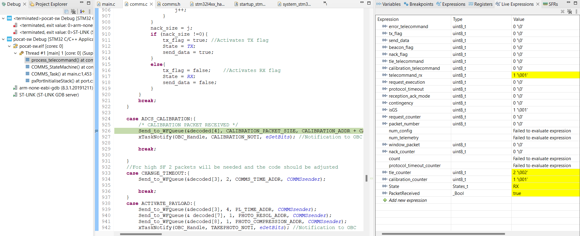
On the one hand, to test the telecommands which don't have a response from the PocketQube, a breakpoint must be placed in the PocketQube code to check if the encoding and decoding have been successful: 
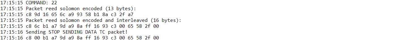
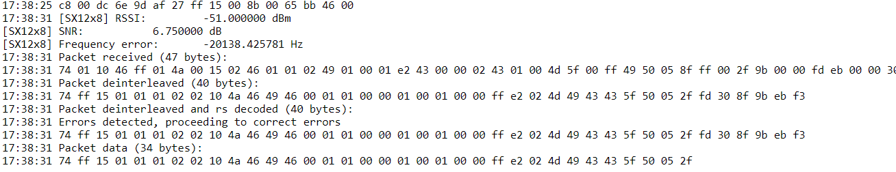
On the other hand, to test telecommands with a response from the PQ, in particular, Send Telemetry and Send Config no breakpoint is needed, because the response is shown in the TinyGS terminal: In this picture, the blue rectangle is the PQ response. The green bytes correspond to a byte corrected thanks to Reed Solomon (it was a forced error).
Then this packet is sent to the MQTT broker as well and then it can also be seen in the TinyGS web app  Note that this packet is classified as a Norby packet and it is supposedly located below New Zealand which are false statements. This is because the Kaity structure of the NanoSatLab PocketQube has still not been sent to the TinyGS team, so the TinyGS decoder does not know how to interpret the information provided in the packet.
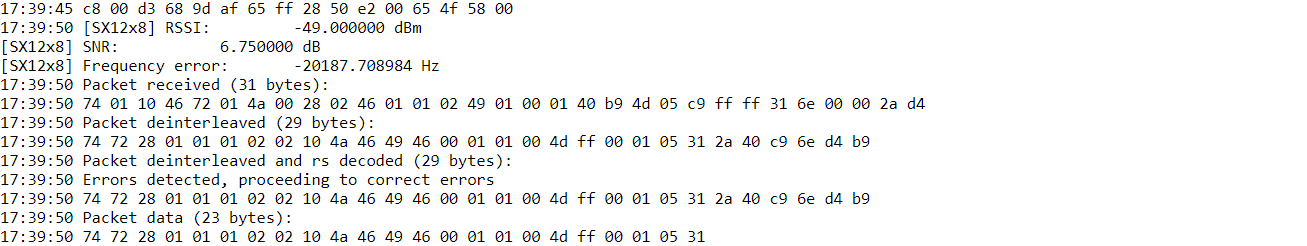
In case of not being able to properly receive the telemetry or configuration, a NACK packet is sent to inform the satellite that a retransmission is needed. To test it, a CRC error has been forced. 
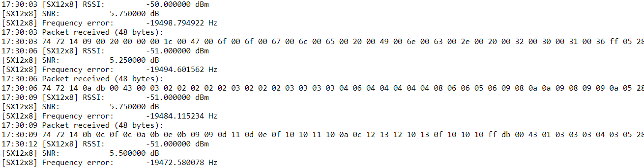
And finally, to test the Send Data, a lot of packets are sent in a row (without encoding): 


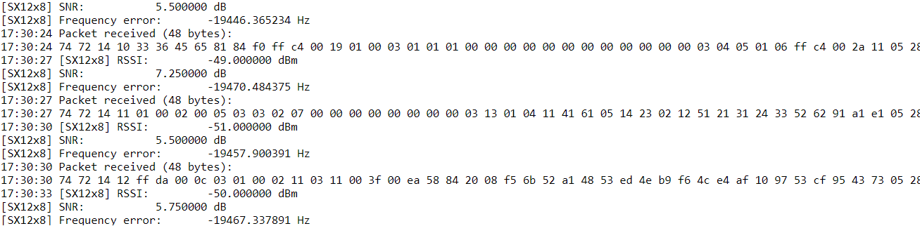
After all the packets are received, an ACK packet is sent to the PQ indicating which packets were properly received. It can be noted that the second packet is not properly received since there is a CRC error. In the ACK packet, after the header (which has 3 bytes), comes a vector with a length equivalent to the number of packets sent. If a packet is not received correctly, the byte with the index equal to the number of the packet failed is 0x0, otherwise, is 0x01. This is why the second byte of this vector is 0x0, because the second packet failed in this case.
Once the PocketQube receives the ACK, it sends back the requested packets. As can be noted, at the bottom of the last figure, the satellite has retransmitted the ordered DATA packet. It is known that this retransmitted packet is the corrupted one because its third byte (the data packet counter) is equal to 0x01, hence taking into consideration that the data packet counter starts at 0x00, this is the second packet.
None.
We are capable of establishing a communication between a Ground Station and a STM32 Nucleo + LoRa module (simulating the PocketQube).
The goal of this test is to validate the proper functioning of the ADCS calibration function, ensuring that the magnetometer is accurately calibrated as anticipated.
| Requirement ID | Description |
|---|---|
| ADCSCAL - 01 | The ADCS calibration telecommand is correctly received and processed. |
| ADCSCAL - 02 | The instruments of the ADCS subsystems are correctly calibrated. |
The test setup for this experiment is straightforward:
Establish a connection between the OBC-COMMS and ADCS boards, enabling seamless information transfer from COMMS to the ADCS subsystem.
Prepare a ground station, with the option to use attenuators to replicate space conditions, we will be sending the telecommand from here.
Following successful calibration, employ a rotating machine to simulate the satellite's rotation in all directions. All data will be read using a computer.
The sole instrument undergoing calibration is the magnetometer. To assess its accuracy, we can perform rotations in all directions and examine whether the obtained results form a perfect sphere. Successful calibration is indicated if the data conforms to a spherical shape; conversely, a lack of conformity signifies an unsuccessful calibration.
Step one involves establishing communication between the ground station and our PocketQube. To achieve this, we will follow the steps outlined in several previous tests, as explained in the preceding test or the RX-TX test.
Upon establishing communication, the next step is to send the ADCS calibration telecommand. To verify the correct reception and execution of the ADCS calibration, breakpoints can be strategically placed within the process telecommand function for monitoring.
Upon receiving the telecommand and uploading the calibration, the success of the calibration can be demonstrated by measuring the magnetometer in all three axes. The results can then be plotted using a computer, and a successful calibration is indicated by the formation of a perfect sphere in the plotted data. For rotating at a constant rate we can use a rotating wheel.
The objective of this test is to prove that the recent modifications of the code have solved the issue we had regarding the reception and registering of longer than 3 packet telecommands.
| Requirement ID | Description |
|---|---|
| MULPT - 01 | Be able to transmit all packets using a TinyGS. |
| MULPT - 02 | Be able to receive and register all the packets. |
Prepare the ground station and Nucleo + LoRa, as explained in previous tests (TinyGS test for example). If we choose to use the OBC-COMMS board instead, the setup should be the following:

If the stipulated conditions are fulfilled, specifically, successful transmission, reception, and registration of telecommands with multiple packets, we will deem this test as successful. The telecommands that satisfy these criteria include the transmission of TLE telecommands and the execution of ADCS calibration telecommands.
Once the Ground Station and the receiving component of our system (either STM32 Nucleo + LoRa or the OBC-COMMS board) have been set up, the remaining task is to transmit either the TLE telecommands or initiate the execution of ADCS calibration telecommands.

Once the telecommand is sent the COMMS subsystem should be receiving the telecommand (if not, check RX-TX test in COMMS SSV testing).
Once the telecommands are received we can check that they have been registered as planned using the Utility program (the one we use to check registers).
Both telecommands can be sent by the ground station.
Still cannot solve the issue where only a part of the packets are reveived. No appearing problem with the reception buffer.
Possible solution is to separate the TLE telecommand in 2 separate telecommands, a first part with 3 packets and a second part with 2 packets. Test will need to be redone.
Currently, the telecommand contents are hardcoded, which is not ideal. The goal is to enable the modification of telecommand contents without the need for code recompilation. Changes were made to the code to address this issue, and this test plan aims to demonstrate the effectiveness of these modifications.
| Requirement ID | Description |
|---|---|
| NHTT - 01 | Transmission of the telecommands is done correctly. |
| NHTT - 02 | Reception and processing of the telecommands is done correctly. |
| NHTT - 03 | Registers are uploaded. |
Set up both the ground station and reception modules according to the instructions provided in the previous tests.
The success criteria for this test involve the accurate transmission, reception, and correct processing of telecommands. The test will be deemed successful if these tasks are executed correctly.
After preparing the ground station and the COMMS subsystem we can begin transmiting the telecommands.
After receiving and processing the telecommands, the next step is to verify the accurate storage of information by the On-Board Computer. It is essential to ensure that the information is stored efficiently and that the addresses of the stored values are no longer hardcoded. To perform this verification, tools such as "Utility" can be employed to inspect the registers and confirm the correct storage of information.
The objective of this test is to take a picture with the VGA Camera (P/L1), ask for it through a telecommand (SEND_DATA), and receive it successfully. The test will be done without the use of TinyGS as it was suspected it was a source of errors (MQTT).
| Requirement ID | Description |
|---|---|
| VCT - 01 | Take a picture with the VGA Camera connected to OBC-COMMS. |
| VCT - 02 | Receive a TTL (SEND_DATA) and execute it. |
| VCT - 03 | Be able to receive the data sent. |
Prepare the OBC-COMMS PCB + Lateral Board, as explained in previous tests, and the CubeCell, acting as our ground station. The VGA should be connected to the OBC-COMMS PCB directly.
The test is considered to be passed as long as a picture is taken, sent after the reception of a TTL, and received by the ground station with no packet loss.
The code will begin by taking a photo with an approximate length of around 9kB, which is the amount of data expected to be able to transmit during a pass. (0x11,0xFF).
The TTL will be send through the CubeCell and executed by the OBC-COMMS PCB.
The packets will be received in the GS and then decoded (removal of headers and non picture information) in order to recover our photo.
The photo was succesfully taken.
The TTL was sent, received and executed (TX of data).
Data was successfully received and decoded, yielding the exact same picture as taken.


Original picture of some members of the PoCat team. Received picture through the procedure.
There seems to appear some issues to enter the COMMS Task if the Flash task is active, commenting the flash task doesn't affect the process and allows for the execution of the test seamlessly. This issue is to be revised thoroughly.
The COMMS-OBC is proved be able to execute a payload task and to provide lossless data transmission under the aforementioned conditions. Further testing with attenuation is required so as to simulate real conditions. The test is successfully passed.
The objective of this test is to prove that data share between PQ2 and PQ3 is possible. The test will be conducted with an OBC-COMMS PCB and a Nucleo Board, as no extra PCB's are available at the moment. It is a preliminary test, and further work should be done.
| Requirement ID | Description |
|---|---|
| CCT - 01 | Be able to transmit a telecommand through the OBC-COMMS. |
| CCT - 02 | Be able to receive said telecommand in the Nucleo and execute it properly. |
| CCT - 03 | Be able to receive the data sent by the Nucleo Board in the OBC-COMMS. |
Prepare the OBC-COMMS PCB + Lateral Board and Nucleo + LoRa, as explained in previous tests (TinyGS test for example). They should be separated by at least 30cm, in this case both systems were connected to different computers. A small code stub in the OBC-COMMS was developed so as to send the TTL.
If the stipulated conditions are fulfilled, specifically, successful transmission and reception on both sides, without any packet loss, the test will be considered passed
Send the SEND_DATA telecommand packet through OBC-COMMS.
We expect to receive the TTL and execute it properly, sending the designated data.
We expect to receive the data sent by the Nucleo and store it in a buffer in the OBC-COMMS Board.
Telecommand was successfully sent.
Telecommand was successfully sent and executed.
The sent data was partially received, missing some of the initial packets.
Communication between two OBC-COMMS Boards should be feasible as proved by this test. Despite that, the test wasn't passed as in ideal conditions not all packets were received. Further investigation, with a more realistic setup and different code proposals are required.
The objective of this test is to prove that frequency switching is possible, without a complete reset of the transceiver.
| Requirement ID | Description |
|---|---|
| FST - 01 | Be able to transmit in our main frequency (868MHz). |
| FST - 02 | Be able to switch transmission frequency and transmit on it (870MHz in these case). |
| FST - 03 | Be able to receive the data sent in both frequencies. |
Prepare the OBC-COMMS PCB + Lateral Board, as explained in previous tests, and the CubeCell, acting as our ground station. They should be separated by at least 30cm. The lines implemented at the beginning of the COMMS loop were:

Note the delays in order to ensure packets are fully sent. In a real case the switching will be done when not transmitting so it shouldn't be a necessary constraint.
If TX frequencies are switched and packets can be received in both of them the test will be considered passed.
Data was successfully sent and received in 868MHz
No measurable changes.
Data was successfully sent and received in 870MHz
The same test was done with less delay, and no frequency switching was observed, probably due to the fact that packets weren't fully sent.
Frequency switching was successfully executed and the test is considered passed.
