Attitude Determination and Control System (ADCS)
Subsystem Description
Document scope
In satellite systems, the ADCS is essential to maintain the proper orientation and stability of the spacecraft. This section will initially present the ADCS of the project, presenting some inicial concepts needed for understanding the theory and finishing with some requirements and the physical architecture of the ADCS with other subsystems.
State of the art
The limited space and power constraints of the PocketQubes pose significant challenges for the design and implementation of subsystems, particularly the ADCS. Thanks to the rapid development of micro-electronics, micro electromechanical systems and integrated circuits, the miniaturization of PQ technology is accelerating.
The ADCS is formed by the attitude determination part, which is the responsible of determine the 3D orientation of the PQ. It uses sensors to obtain information about the environment to determine its orientation. The most common sensors used are magnetometers, Sun sensors, earth sensors, gyroscopes and star trackers. The ADCS that has been developed in this project, is formed by a gyroscope, a magnetometer and photodiodes used as Sun sensors.
Concerning attitude control, it can be achieved passively using magnets located inside the PQ and gravity-gradient stabilization. Additionally, active attitude control can be implemented with actuators such as reaction wheels or magnetorquers. Magnetorquers are the most common actuators used in PQ and will be used in this project. Because of the extremely tight available space, they will be incorporated into the internal layers of the Solar Panels PCBs.
Initial concepts
Coordinate reference frame
In order to understand this subsystem, some terms must be defined:
- Frame: Coordinate system of the 3D space that follows the right-hand rule.
- Body frame: Cartesian frame with its origin at the centre of mass of the satellite.
- Reference frame: A determined known frame.
- vb: Representation of vector v in the body frame.
- vr: Representation of vector v in the reference frame.
It is recommended for the reader to understand a vector as a unique entity in the 3D space. It is essential to distinguish between the vector entity, and the representation of the vector with respect to a frame. The representation of the vector will vary depending.
Inertial frame
As an inertial frame, the Earth Centered Inertial frame (ECI) will be used. It is a global cartesian reference frame that has its origin at the center of the Earth. 
- X axis points to the Vernal Equinox.
- Y axis completes the set with the right-hand rule.
- Z axis aligned with the Earth’s rotation axis.
Figure 1: ECI frame chematic
Body frame
The body frame will have its origin at the centre of the PocketQube. The axis definition is the following:
- X axis aligned with the PocketQube width, parallel to the sliding plate and perpendicular to the direction of
insertion into the PocketQube deployer. - Y axis aligned with the PocketQube height direction, pointing upwards from the sliding plate.
- Z axis aligned with the PocketQube length, the direction of insertion into the PocketQube deployer and
completing the right handed reference frame.

Figure 2: Satellite body frame schematic
Quaternions
Quaternions are a mathematical concept equivalent to a rotation matrix. They are used in software for their computational efficiency and to avoid singularities. According to Euler’s Theorem, any rotation is a rotation about a fixed axis, which is represented by the unit vector 𝐞. The angle of rotation is represented by 𝜃. In other words, for any rotation matrix 𝐀, there is a unique 𝐞 and 𝜃 that uniquely define the rotation with respect to the right-hand convention. A quaternion 𝐪 is a four-dimensional vector where the first component is called the scalar part, and the last three components are the vector part. The quaternion is related to the Euler axis-angle in the following manner:

If 𝐴𝑖𝑗 is the element of 𝐀 in its 𝑖-th row and 𝑗-th column, then:


Therefore, a quaternion 𝐪 can be expressed as a function of its rotation matrix 𝐀 using these properties:

Where 𝜀 is the vectorial part of the quaternion. Note that if 𝜃 = 180º, the vector 𝐞 is indeterminate. In such cases, 𝐞 is parallel to any non-zero column of 𝐀. Additionally, it’s crucial to maintain the sign convention.
For any rotation matrix, there exist two corresponding quaternions that differ only in sign. For instance, a rotation of 𝜃 = 180º and another of 𝜃 = 540º are equivalent, but the resulting quaternions are opposite. To uphold the sign convention, it’s necessary to ensure that the scalar part is positive, i.e., to enforce 𝜃 ≦ 180º. This is achieved by changing the sign of the entire quaternion if the scalar part is negative.
There is an essential property for achieving attitude control in the ADCS. If there are two quaternions, q1 and q2, and q1 is conjugated and then multiplied by q2, the resulting quaternion represents the relative rotation between the two quaternions.

In this case qerror would be the quaternion that represents the rotation needed to align q1 to q2. The qerror can also be named error quaternion.
Orbital propagator
An orbital propagator is used to determine the position and velocity of the satellite at a given instant of time, given by the initial position of the satellite and the velocity at this position. In the satellite we are using the J2 propagator, whose main property is
that it accounts for the Earth’s oblateness while propagating the orbit. Additionally, this propagator is ideally for our PQ because of the balance of memory requirements and complexity fits in the OBC.
There are more precise orbital propagators like the SGP4 model which accounts for atmospheric drag and other secular effects apart from the Earth oblateness, but it is much more complex, and it requires more memory than the one available in our satellite.
Geomagnetic field model
The geomagnetic field model is essential for calculating the Earth’s magnetic field at specific coordinates and dates. This model helps to understand and predict the variations in the Earth’s magnetic field. In this work, the IGRF model is used, but simplified up to order 2 , commonly referred to as the Tilted Dipole model. The Tilted Dipole model approximates the Earth’s magnetic field as a dipole that is tilted relative to the Earth’s rotational axis. Despite its simplicity, this model provides a reasonably accurate representation of the geomagnetic field for many practical purposes. The coefficients for the Tilted Dipole model are derived from the IGRF model, which is updated every five years based on satellite and ground-based observations .
Functional architecture

Figure 3: ADCS functional architecture schematic with the rest of the subsystems
The ADCS in the PocketQube serves as an interface between the outer boards and the inner PCBs of the satellite. As shown in [Figure 3], the ADCS is connected to three main structural components: the outer boards, the inner +Y magnetorquer PCB, and the on-board computer (OBC).
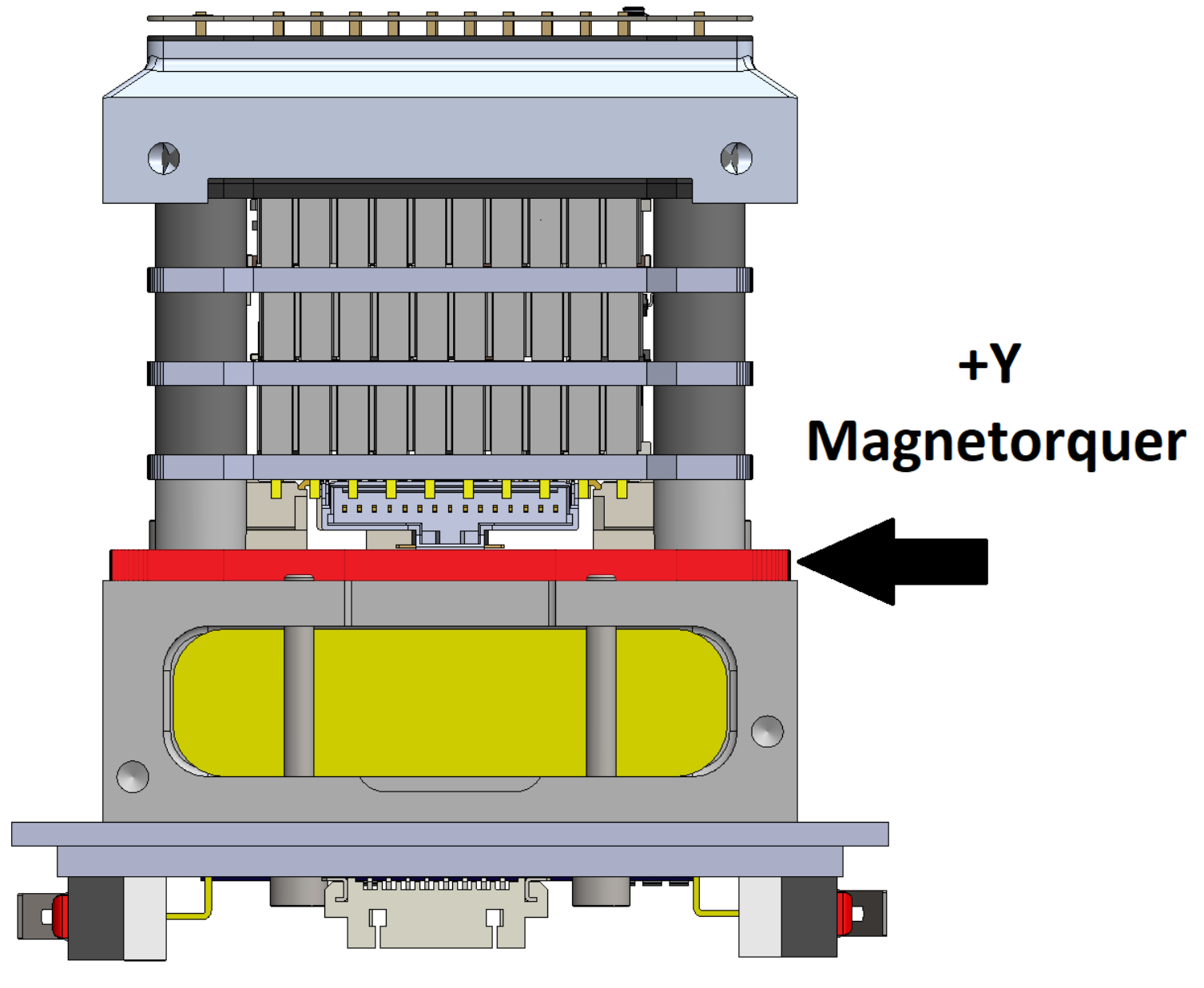
On the outer boards, there are magnetorquers used for the ±X, -Y, and ±Z axis, photodiodes, and some temperature sensors. Additionally, the +Y magnetorquer is connected just below the ADCS PCB. This location is chosen due to space constraints within the PocketQube, as it is not optimal to place it on the top board, where the payload will be inserted.
Finally, the ADCS is connected to the OBC, which is responsible for processing all data gathered by the ADCS. The connections between the ADCS and the OBC are not simple power lines each has a specific function:
- I2C conection: This connection is primarily used for transmitting data from the sensors to the OBC using the I2C protocol, enabling full-duplex communication between the sensors and the OBC.
- GPIOD conection: The GPIOD is an output from the OBC used to send signals of 0 volts or 3.3 volts. In the ADCS, it serves as an input for the multiplexer.
- Analog to digital converter (ADC): This is an input to the OBC used to convert the signal from the operational amplifier multiplexer into a digital value.
Requirements
| SS | ID | DESCRIPTION |
|---|---|---|
| ADCS | ADCS-0000 | The communication between the chips of the ADCS and the OBC must be conducted via I2C. |
| ADCS | ADCS-0010 | The PQ must be able to detumble using the BDOT algorithm. |
| ADCS | ADCS-0020 | The satellite must be able to point the Payload at the nadir angle using the magnetic control law. |
| ADCS | ADCS-0030 | The ADCS must be able to estimate the satellite's position in an inertial reference frame. |
| ADCS | ADCS-0040 | The ADCS must be able to obtain the magnetic field in an inertial reference frame. |
| ADCS | ADCS-0050 | All sensors used in the ADCS must be calibrated and characterized by temperature. |
| ADCS | ADCS-0060 | The magnetorquers must have a reliable current supply to ensure optimal performance. |
| ADCS | ADCS-0070 | The ADCS must have a fail-safe mechanism to enter a safe mode in case of anomalies. |
| ADCS | ADCS-0080 | The ADCS sensor's calibration parameters must be able to be modified via telecommand. |
Hardware Design
Introduction
The hardware of the Attitude Determination and Control System (ADCS) is essential for the satellite’s operation. Without it, the satellite would be unable to gather critical data about its orientation and environment in space, which is necessary for executing various functions. The ADCS hardware enables the satellite to determine its position, control its orientation, and stabilize itself, ensuring that it can carry out mission objectives such as data collection and communication.
Design Choices
The design of the ADCS follows a simple philosophy, all components and sensors are selected for their low power use, good performance, and reasonable cost. The goal was to choose parts that are reliable and fit within the PocketQube’s limited power and budget.
Actuator selection
There were several options for implementing an actuator in the PocketQube. As explained in the ADCS introduction section, there are two ways to achieve attitude control: passive control, using a magnet as an actuator, and active control, using reaction wheels or magnetorquers.
The passive option was considered, as it is the primary method used for achieving attitude control. However, one drawback of this approach is the limited control over pointing precision.
For the active option, using reaction wheels was discarded because the size and power consumption requirements of a PocketQube are incompatible with this approach. Thus, the remaining option for active attitude control was the magnetorquers. This technique is relatively new, and this would be one of the first PocketQubes to implement it. Additionally, it offers the pointing accuracy needed to conduct the required measurements. For these reasons, magnetorquers were chosen.
Sensors election
Regarding the sensors, the main objective was to find ones compatible with the I2C protocol.
Why the I2C protocol is the selected in the Satellite?
The I2C protocol is mainly used for enabling communication between multiple integrated circuits on the same board with minimal wiring. It is based on a two-wire serial communication protocol, which uses one line for data, called SDA, and another for the clock signal, called SCL, allowing for simple, low-speed data exchange over short distances.
I2C is used in applications where several peripheral devices (like sensors, memory devices, or display drivers) need to communicate with a central microcontroller or processor. It also has low power consumption, which is crucial in satellite applications.
2.2.1 Magnetometer
The magnetometer IC that will be used for the ADCS is the MMC5983MA, developed by MEMSIC, is a high-precision, 3-axis magnetometer known for its small size and low power consumption, making it particularly suitable for small satellite applications like PocketQubes. Datasheet: MMC5983MA
|
Attribute |
Specification |
|---|---|
|
Name |
MMC5983MA |
|
Supplier/Manufacturer |
Mouser, Memsic |
|
Power Consumption |
212.19 μW |
|
Field Range |
± 8 G |
|
Resolution |
0.25 mG per LSB |
|
Operation Bits |
16 bits |
|
Sensitivity |
± 4096 Counts/G |
|
RMS Noise |
0.4 mG |
2.2.2 Gyroscope
The Gyroscope IC that will be used for the ADCS is the IIM-42652, manufactured by TDK InvenSense, is a compact, high-performance 6-axis Inertial Measurement Unit (IMU) combining a 3-axis accelerometer and 3-axis gyroscope. Its design and capabilities make it well-suited for small satellites like PocketQubes, which require efficient, low-power, and reliable orientation and motion data for various tasks such as attitude determination, stabilization, and control. Datasheet: IIM-42652
|
Attribute |
Specification |
|---|---|
|
Name |
IIM-42652 |
|
Supplier/Manufacturer |
Mouser, TDK InvenSense |
|
Power Consumption |
1.91 mW |
|
Scale Range |
±15.625 °/s, ±31.25 °/s, ±62.5 °/s, ±125 °/s, ±250 °/s |
|
Operation Bits |
16 bits |
|
Sensitivity Scale Factor |
2097.2 LSB/(°/s), 1048.6 LSB/(°/s), 524.3 LSB/(°/s), 262 LSB/(°/s), ç 131 LSB/(°/s) |
|
RMS Noise |
0.038 °/s-rms |
2.2.3 Temperature Sensors
The temperature sensors that will be used are named TCN75A, createdby Microchip Technology, designed for low-power applications and precise temperature measurement. Its compact size, low power usage, and simplicity make it suitable for use in small satellite platforms like PocketQubes, especially where basic thermal monitoring is needed. Datasheet: TCN75AVOA
|
Attribute |
Specification |
|---|---|
|
Name |
TCN75A |
|
Supplier/Manufacturer |
Mouser, Microchip Technology |
|
Power Consumption |
1.65 mW |
|
Field Range |
-40 °C to 125 °C |
|
Accuracy |
±1 °C |
|
Resolution |
0.0625 °C to 0.5 °C |
|
Operation Bits |
16 bits |

2.2.4 Photodiodes
The SLCD-61N8 is a reliable and cost-effective silicon photodiode designed for light sensing and power generation. It provides visible to infrared sensitivity, high efficiency, low capacitance, and excellent durability. The choice of photodiode is flexible, and alternative models with similar wavelength sensitivity to sunlight can also be considered for use. Datasheet: SLCD-61N8
|
Attribute |
Specification |
|---|---|
|
Name |
SLCD-61N8 |
|
Supplier/Manufacturer |
Mouser, Advanced Photonix |
|
Short Circuit Current |
170 μA |
|
Open Circuit Voltage |
0.4 V |
|
Maximum Sensitivity Wavelength |
930 nm |
|
Acceptance Half Angle |
60 deg |

PCB Design
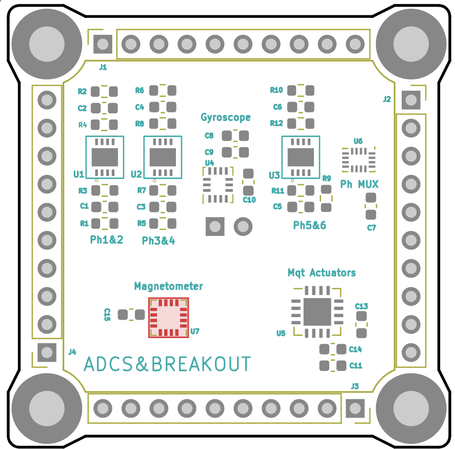
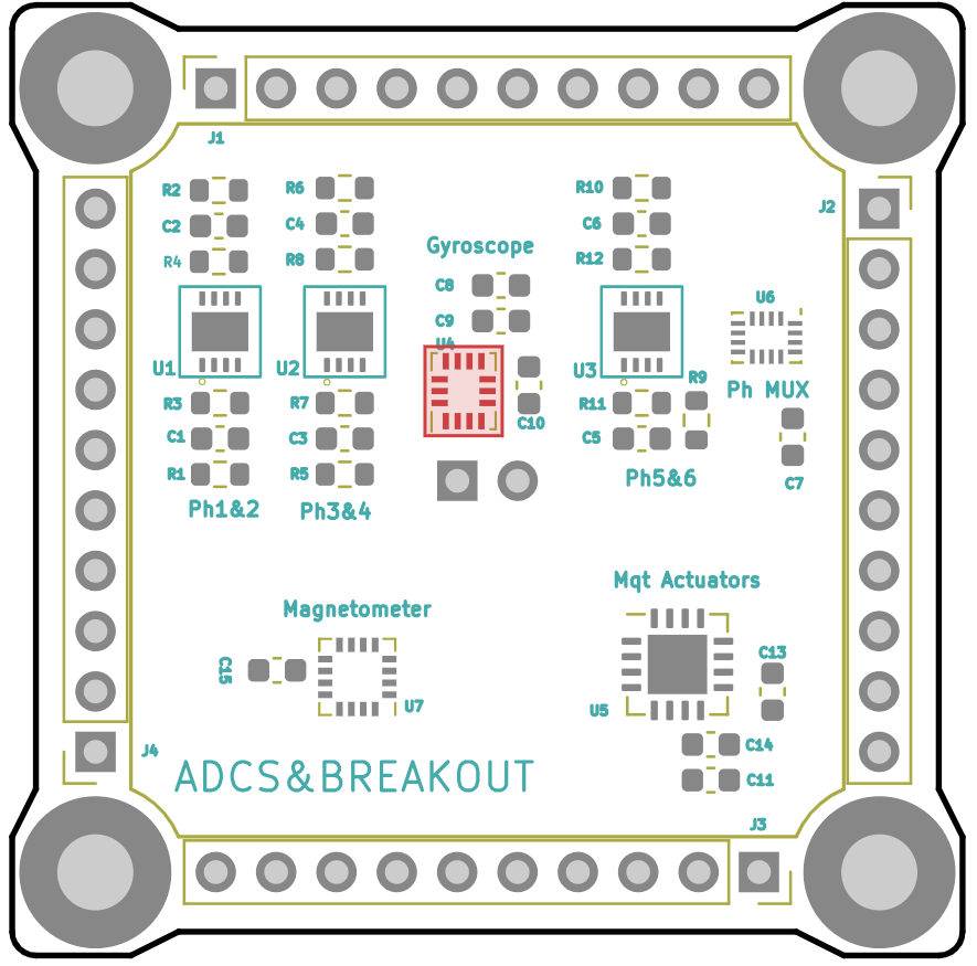
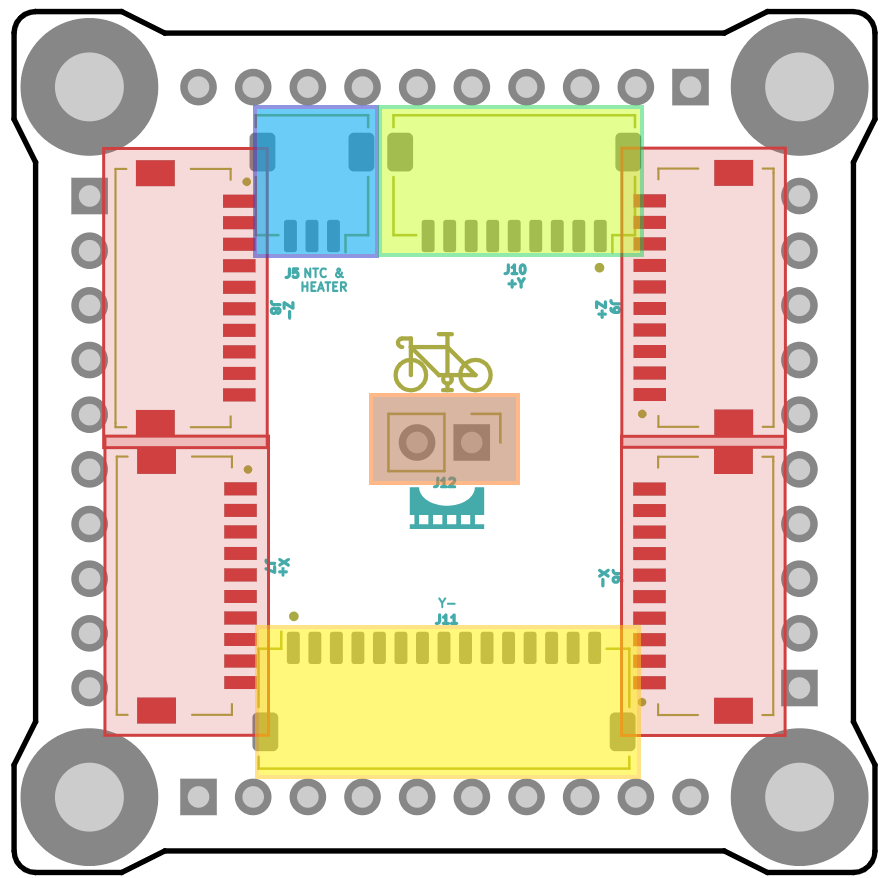
This is the PCB design of the ADCS. The board is also used as an interface between the other subsystems and the outer boards and the battery. It is divided into 5 different blocs.

- Photodiode block: This block is responsible for receiving information about the sunlight received on the surface of the PocketQube. A photodiode is located on each lateral board, as well as on the top and bottom boards. Each photodiode receives sunlight and generates a current in response. This current is amplified using an operational amplifier, which also converts the intensity into voltage so it can be read by the Analog-to-Digital Converter (ADC) of the On-Board Computer (OBC). The OBC in order to select a photodiode to read, it controls a multiplexer used for selecting the output of a specific operational amplifier.
- Gyroscope block: This section of the PCB is in charge of obtaining the information about what angular velocity is rotating the satellite in all three axis. It is formed by the IIM-42652 chip and some resistors.
- Magnetometer: This part of the PCB serves to measure the value of the magnetic field at the PocketQube coordinates. The chip used is the MMC5983MA and is accompanied by a capacitor.
- Magnetorquer driver: This chip is the responsible for providing the selected current to the magnetorquers. In order to make the chip work, a LED has been added for each magnetorquer in its outer board. The IC used is the BD2606MVV followed by three capacitors.
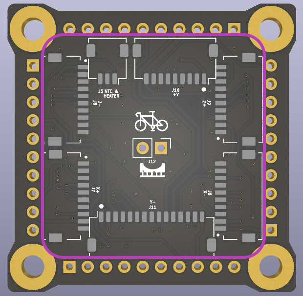
- Bottom connectors: In the backside of the PCB there are located 7 connectors. These connectors are used as an interface for each outer board of the Satellite. These pins contains the Photodiodes inputs and the magnetorquer connexions. In addition it also is used for connecting the temperature sensors located in the outer boards to the OBC and for connecting the battery heater and the battery temperature sensor.
Full schematic

Passive components
Integrated circuits
|
Component |
Type |
Quantity |
Manufacturer number |
Connectors
|
Component |
Type |
Quantity |
Manufacturer number |
A more detailed information about each vertical PIN and bottom pin is shown in the following picture:
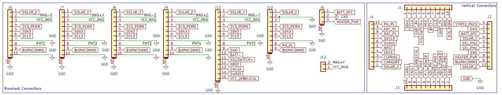
- Connectors J6,J7,J8 & J9: These connectors are used for the lateral boards and serve multiple functions. The pins include the following: the input for the voltage generated by the solar cells (SOLAR_X), the input and output for the magnetorquers (VCC_MAG and MAG ‘±X ±Z’), the I²C communication buses (SDA and SCL), the input for the photodiode, and an output for injecting the required voltage into the resistor used for antenna deployment. This output (BURNCOMMS) is utilized if the antenna is placed on the corresponding lateral board.
- Connector J10: This connector is used for the top payload. If the a new payload is being developed, the obligatory pins needed are the Photodiode PIN and its corresponding ground pin. The rest of the PINS can be modified according to the requirements of the new payload. In case of using the OpenPOcketQube Kit paylaods, this connector is used only in the VGA camera.
- Connector J11: This connector is used for the bottom board it has included the same pins as the J6, J7, J8 & J9 connectors, but including some new ones. The functionalities of the new pins are the following: BATT- & KILLSWITCH+, used for activating the EPS after the deployment of the satellite. Also the pins used for debuging the satellite using the umbilical connector located at the bottom PCB are located in J11 (NRST, SWCLK,SWDIO & VCC umbilical). Finally, there is the SWO pin, which can be used for any functionality, it is a programable pin.
- Connector J5: Connector used for the battery heater and temperature sensors located in the battery compartment.
- Connector J12: Used for connecting the magnetorquer +Y PCB located under the ADCS.
Magnetorquer actuators
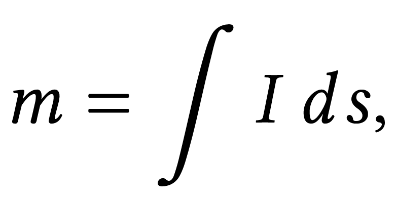
The magnetorquers are responsible for achieving attitude control in the PQ. These devices function as magnetic dipoles and when an electric current is passed through them, they create a magnetic moment. This magnetic moment interacts with the Earth’s magnetic field, generating a torque that adjusts the satellite’s orientation. This interaction can be represented as:
![]()
The calculation of the magnetic moment depends on the type of magnetorquer used. In the PocketQube, planar helical coils serve as magnetorquers, embedded in the outer boards along each axis, except for the +Y axis, where they are positioned within the inner layers of the satellite. These coils are distributed across the boards in four layers.

Magnetorquer characteristics
|
|
+Y PCB |
Lateral & Bottom |
|
Separation between turns |
0.2 mm |
0.2 mm |
|
Height |
35 µm |
35 µm |
|
Width of the trail |
0.18 cm |
0.18 cm |
|
Material of the trail |
Copper |
Copper |
|
Dimensions |
28 x 28 mm |
32 x 32 mm |
|
Resistance |
89.91 Ω |
88.3 Ω |
|
Turns per layer |
42 |
38 |
|
Maximum moment |
3.63·E03 a·m^2 |
3.2·E03 a·m^22 |
Magnetorquer injected current formula derivation
In order to compute the intensity, firstly the total magnetic moment expression shall be derivated. The magnetic moment of a coil is,
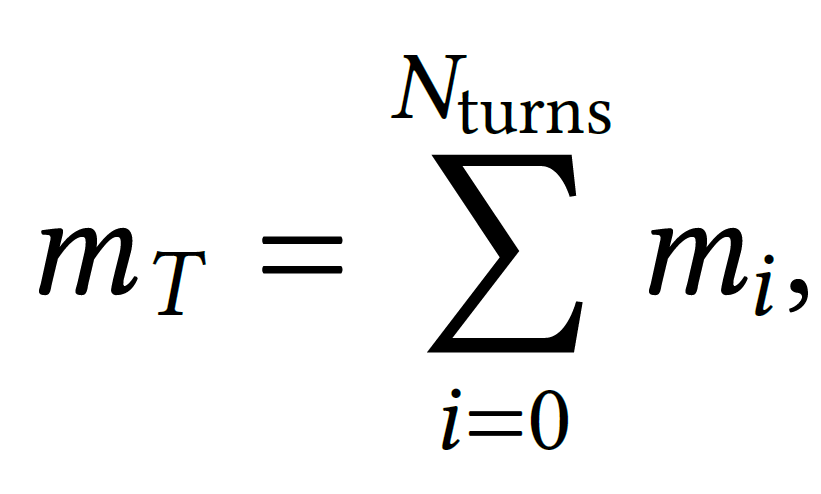
As we have a combination of coils the total magnetic moment will be,
To compute the total magnetic moment, the magnetorquer coils will be modeled as square coils, with each turn represented as an individual square coil,
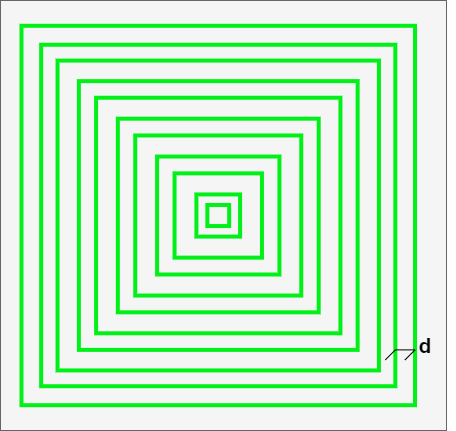
These coils are separated by distances 𝐝outer = 0.2 mm and 𝐝top = 0.18 mm. The label, "outer" refers to the magnetorquers located on the outer boards, and the label "inner" refers to the magnetorquer located inside the satellite.
The total magnetic moment of the magnetorquers will be computed as:
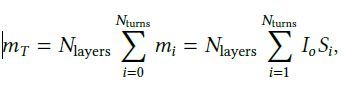
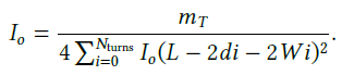
Where 𝐍layers is the number of layers of the magnetorquer, 𝐈o is the required injected intensity, and 𝐒𝐢 the surface ofthe coil with the turn number 𝐢. The expression that calculates the surface of each turn is:
![]()
where 𝐋 is the size of the bigger coil and 𝐖𝐢 the amplitude of the conductor of the coil. In addition 𝐝𝐢 and 𝐖𝐢 can be 𝐝𝐢(𝐢𝐧𝐧𝐞𝐫), 𝐝𝐢(𝐭𝐨𝐩), 𝐖𝐢(𝐢𝐧𝐧𝐞𝐫), 𝐖𝐢(𝐭𝐨𝐩). Isolating the required current from the equation we obtain that:
Magnetorquer polarisation
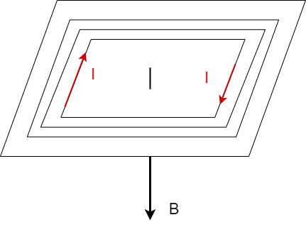
Finally one of the most important things to characterize of the magnetorquers is their polarisation. The polarisation of a coil refers to the direction of the magnetic fiel generated when some intensity is injected throught the coils. The polarisation should follow the right hand rule.
In our case as shown in,
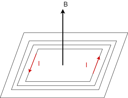
If the current flows clockwise, the magnetic field direction is perpendicular towards the bottom face of the plane formed by the coils of the magnetorquer. Similarly, if the current flows counterclockwise, the magnetic field direction is perpendicular towards the top face of the plane,
Software Design
The software of the Attitude Determination and Control System (ADCS) is equally essential for the satellite’s operation. Without it, the satellite would lack the intelligence to interpret critical data about its orientation and respond to its environment in space, which is necessary for executing various functions. The ADCS software processes sensor data, executes algorithms to determine the satellite's position, and issues commands to control and stabilize its orientation. This ensures that the satellite can reliably carry out mission objectives such as precise data collection, alignment with targets, and consistent communication.
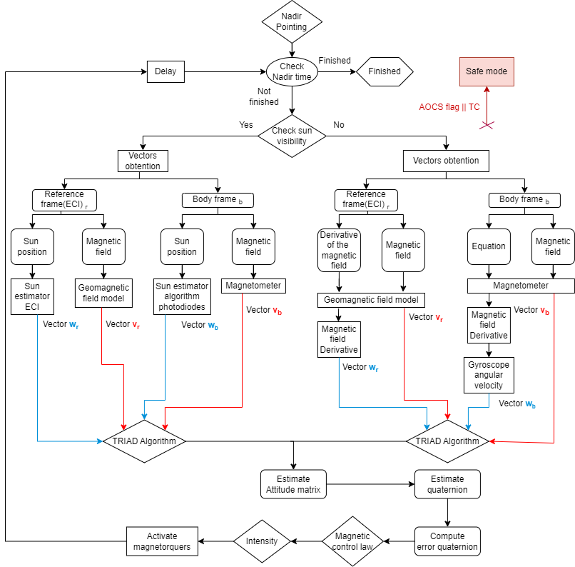
Attitude determination
The attitude of the satellite is represented mathematically as the rotation matrix, which stores the information about the orientation of the satellite. The objective of the ADCS is to calculate that matrix and later conduct some functionalities to achieve the desired orientation.
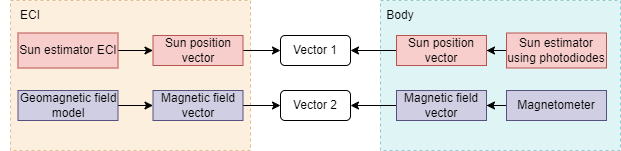
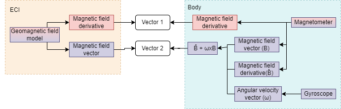
To calculate the rotation matrix, the idea is to obtain two type of vectors, each one of them represented in two different frames, the ECI and the body frame. Once we obtain these vector the following system of equations shall be solved :
 where subscript 1 represents the first vector, subscript 2 represents the second vector, r denotes the reference frame, and b denotes the body frame and the symbol A refers to the rotation matrix. Since this system of equations is undetermined, the rotation matrix cannot be directly computed and must be estimated. In order to estimate it, the TRIAD algorithm will be used.
TRIAD algorithm
The TRIAD algorith is based on the assumption that one of the unit vectors is much more accurately determined than the other. It denotes that 𝐛𝟏 is much more accurated than the others. The estimation of the rotation matrix is shown in,
![]()
![]()
Vector election criteria
The criteria chosed to select the vectors is the following one:
- The first case is when we have Sun exposition. In this case we will use the magnetic field vector and the Sun position vector. From the magnetic field vector, the body frame vector will be obtained from the magnetometer, and the reference frame vector will be obtained by the geomagnetic field model. In terms of the Sun position vector, the body vector will be estimated using the photodiodes and the temperature sensors of the PQ. The vector from the reference frame will be obtained by an ECI Sun estimator algorithm.The first case is when we have Sun exposition. In this case we will use the magnetic field vector and the Sun position vector. From the magnetic field vector, the body frame vector will be obtained from the magnetometer, and the reference frame vector will be obtained by the geomagnetic field model. In terms of the Sun position vector, the body vector will be estimated using the photodiodes and the temperature sensors of the PQ. The vector from the reference frame will be obtained by an ECI Sun estimator algorithm.
- The other case is used when there is not direct exposition to the Sun, i.e when there is eclipse. In this case the magnetic field vector is used like in the previous case, however as the second vector we will use in the reference frame the derivation of the magnetic field and for the body frame the vectorial product between the angular velocity with the magnetic field plus the derivative of the magnetic field will be used.
Attitude Control
ADCS Mode definitions
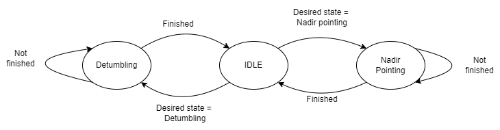
The former AOCS modes of operations available in the PocketQube are the Detumbling mode, Nadir pointing and the IDLE mode. The primary purpose of the ADCS implementation is to prevent unnecessary energy consumption. If no AOCS functions are needed, the task will remain blocked until required, it will be activated by the onboard computer only when necessary.
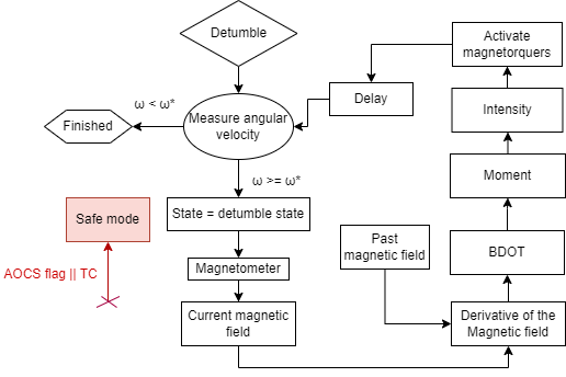
Detumbling mode
After the deployment from the rocket, the PQ is expected to start rotating at an average rate of 30 degrees per second. In addition, the PQ will be influenced by various external forces during its orbit, causing it to start rotating, and intentional rotations will be applied to the PQ to manage its temperature more efficiently. Because of these factors its necessary a functionality that permits to detumble the satellite. This mode will be used in the following situations:
- Stabilizing the satellite after its deployment.
- Stabilizing the satellite after conducting the tumbling functionality.
- Stabilizing the satellite in response to external orbital perturbations that could cause unwanted rotation.
The detumbling mode uses the BDOT controller. For determining the value of the constant used in the BDOT algorithm, the BDOT law method will be used, which uses the maximum magnetic moment that will be generated by the magnetorquers and the sign of the derivative of the measured magnetic field. This maximum magnetic moment is computed taking into account that the maximum intensity that the magnetorquer driver can provide to the magnetorquers is of 32 mA.
![]()
Nadir pointing mode
In order to perform correctly the measurements of the payload antenna, the PQ must be pointing to the Earth. Nadir pointing is the most crucial functionality of the ADCS, because it is the responsible of pointing the satellite to the Earth. For achieving it a magnetic control law is used. It computes the desired magnetic moment using the magnetic field, the angular velocity and the vectorial part of the required quaternion that is needed for rotating the satellite’s quaternion to the required quaternion.
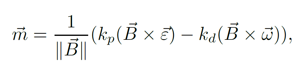
where the constants 𝐤𝐩 and 𝐤𝐫 are obtained from the PID controller, and the 𝜺 represents the vectorial part of the error quaternion.
IDLE Mode
The IDLE mode is the default mode, this mode is always set whenever the AOCS is not running any functionality. In addition, this is the only mode where the On board computer will be able to block the AOCS task to prevent undesired energy consumption.
ADCS Control and determination algorithms
Geomagnetic field model
In the PocketQube, the geomagnetic field model that is implemented is a simple Tilted dipole model. This is due to memory limitations in the PocketQube. The tilted dipole is a simplified model of the IGRF13 with only two coefficients. However, if additional memory is available, the possibility of adding more coefficients will be considered.
| Inputs | Outputs |
| Geodetic coordinates | Magnetic field in ECI [nT] |
| Decimal year |
Orbital propagator
The orbital propagator used for the PocketQube is the J2 orbital propagator. The algorithm estimates the orbit in ECI coordinates using the TLE received from the ground station. Due to memory limitations, this propagator is chosen, but using a more accurate one will be considered if memory permits.
| Inputs | Outputs |
| Satellite TLE | Satellite propagated orbit in ECI |
| Desired propagated time [hours] |
Sun position estimator
In the PocketQube, two different methods are used to determine the sun’s position, one in the ECI frame and another in the body frame. Hence, two algorithms are implemented:
- Sun position estimator in ECI frame: This algorithm estimates the sun’s position in ECI coordinates using the Julian
date.
| Inputs | Outputs |
| Date | Sun position ECI |
- Sun position for body frame:This estimator uses photodiodes placed on the lateral, bottom, and top boards
of the satellite to determine the sun’s position relative to the satellite. The selection of the face receiving the
most sun power is based on two criteria:
- The photodiode on the face must generate current from a light source.
- If two orthogonal faces receive light (due to Earth’s albedo), the face with the highest temperature is selected.
| Inputs | Outputs |
| Received light from photodiodes | Sun position in body frame |
| Temperature of latera, bottom and top boards |
Subsystem Verification (SSV)
DOCUMENT SCOPE
The aim of this document is to explain the subsystem verification tests to carry out on Attitude Determination & Control Subsystem, in order to obtain/discard any anomaly that the subsystem could suffer during the performance of these test.
TEST 1: Electrical check
Test Description and Objectives
The aim of this test is to verify that none of the components or connections were damaged during assembly, ensuring the integrity and reliability of the board. This involves checking for any physical defects or misalignments that could impact performance, as well as measuring electrical parameters to ensure that the components operate efficiently. Conducting this test helps to identify any potential issues that could lead to failure in the field, thereby ensuring the overall functionality and longevity of the assembled device.
Requirements Verification
| Requirement ID | Description |
|---|---|
| ADCS - SSV - 00 | All external physical aspects, such as scratches, soldering, or joint issues, of the PCB must be inspected. |
| ADCS - SSV - 01 | Each lateral pin must establish a secure connection. |
| ADCS -SSV - 02 | All active components must be ensured to operate correctly, with no short circuits or open connections, and each pin, must meet the specified value. |
| ADCS -SSV - 03 | The positioning and fitment of each component mounted on the PCB must be verified. |
Test Set-Up
- ADCS payload full soldered
- Microscope
- Power Supply
- Wires
- Soldering machine
- Tin
- Flux
- Multimeter
- Calculator, pen and paper
- Laptop
Pass/Fail Criteria
In order to pass the test all the requirements must be met.
Test Plan
| **Step ID** | **Description** |
| Test1 - 10 | With the help of the microscope, look at the PCB looking for any outer physical parameters, such as scratches, soldering or joint issues. If any anomaly is detected, re-solder or fix the encountered error. |
| Test1 - 20 | Check the correct connection with the corresponding component of the 40 pins (10 in each lateral side) with the multi-meter. |
| Test1 - 30 | Check the value with the multi-meter of all the passive components and compare it to the one in the schematic. |
| Test1 - 40 | Verify the active components, checking one by one all the pins with the multi-meter in order to find shorts, open ends, and correct connections among the various pins. |
| Test1 - 50 | Check the connections between all of the components and pins of the PCB. |
Test Results
The test for the ADCS PCB has been done during the 09/03/2023.
The test passed the visual inspection since the outer physical checking was successful.
The pins', passive and active components' connectivity were successfully accomplished considering that there were no open ends or shorts, and the component values were correct.
The in-circuit testing was passed since the connections between all of the components and pins of the PCB were verified.
Anomalies
Power Supply problems
Problem encountered: When putting the 3.3V into the 3.3_PERM pin of the PCB, the voltage measured in the pin is not 3.3V. Follow these steps:
- Check the board again with the multimeter searching for any short circuit
- Check the schematic to see if there is any mistake
- If not anomalies are detected, resolder the PCB
Solution:
Once the first two points were made and since the problem was no resolved it became necessary to desolder certain blocks of the PCB, with the operational amplifiers being the first among them. After removing the amplifiers the voltage was tested using a multimeter, marking the needed 3.3V.
Conclusions
The PCB passed the electrical test and is ready to do more complex tests.
TEST 2: GYROSCOPE
Test Description and Objectives
The purpose of this test is to validate that the gyroscope integrated into the PCB operates in accordance with the specified requirements and successfully communicates with the computer using the I2C protocol. This includes assessing the gyroscope's performance metrics and ensuring reliable data transmission between the gyroscope and the computer.
Requirements Verification
| Requirement ID | Description |
|---|---|
| ADCS - SSV - 10 | The gyroscope must be tested using a reliable tool capable of reproducing constant angular velocities accurately. |
| ADCS - SSV - 11 | The gyroscope must be able to switch between specific full scale ranges of angular velocities. |
| ADCS - SSV - 12 | The gyroscope produced bits, must be translated in degrees per second or radians per second. |
| ADCS - SSV - 13 | The data from the gyroscope must closely match the theoretical value corresponding to the rotation of the rotary platform. |
Test Set-Up
- ADCS PCB
- STM32L476RG nucleo board
- Power Supply
- Wires
- Multimeter
- Oscilloscope
- Calculator, pen and paper
- Reliable tool capable of reporducing constant angular velocities. In example a rotating platform with motor.
- Power supply.
- Chronometer, you can use a mobile application
- Desired programming software used, in this test STM32CubeIDE is used
Pass/Fail Criteria
The gyroscope will be verified if the requirements mentioned before are fulfilled. If in one of them it is detected any anomaly it will have to be corrected, otherwise the board can not pass to the other tests.
Test Plan
| **Step ID** | **Description** |
| Test2 - 10 | Connect the power supply to the STM32 nucleoboard. |
| Test2 - 20 | Open the STM32CubeIDE program. |
| Test2 - 30 | Prepare a code that can read from the gyroscope using I2C. |
| Test2 - 40 | Connect the nucleoboard to the ADCS PCB correctly. |
| Test2 - 50 | Run the code into the nucleoboard in the debug mode checking step by step if the connection with the ADCS board is working correctly. |
| Test2 - 60 | Connect the rotating platform with motor to the power supply, inject the voltage and intensity needed for the proper operation of the engine. |
| Test2 - 70 | Place the gyroscope in the rotation platform and run the code. Write down the values of the data. |
| Test2 - 80 | Measure with the chronometer how long the platform takes in rotating 360 degrees, then compute how many degrees per second it is equivalent to. |
| Test2 - 90 | If the values of the gyroscope and the computed value corresponds with the values computed before, the gyroscope is working correctly. |
3.5.1 I2C communication and registers
The device address of the IIM-42652 is AD = 0b1101000X where the last bit "X" is chosen depending in what function we are conducting in the chip register, reading X=1 or writing X=0.
The registers modified and used in the code are the following ones:
| **REGISTER NAME** | **ADDRESS** | **FUNCTION** |
| SENSOR\_CONFIG0 | 0x03 | Disables and enables the gyroscope axis. |
| PWR\_MGMT0 | 0x4E | Enables and disables all sensors of the chip. We are only enabling the temperature sensor and the gyroscope. |
| GYRO\_CONFIG\_STATIC2 | 0x0B | Disables and enables Anti-Aliasing/low pass filter and notch filter. In our case we are using only the Anti-aliasing and low pass filter. |
| GYRO\_CONFIG0 | 0x4F | Configuration register for the gyroscope, the full scale range and the ODR frequency can be modified. We are using the default frequency of the ODR and a full scale range that fluctuates depending on the situation (this can't be configurated via registers, it has to be coded). |
| GYRO\_DATA\_X1/X0 | 0x25/0x26 | X1: Upper byte of Gyro X-axis data. X0: Lower byte of Gyro X-axis data. |
| GYRO\_DATA\_Y1/X0 | 0x27/0x28 | X1: Upper byte of Gyro Y-axis data. X0: Lower byte of Gyro Y-axis data. |
| GYRO\_DATA\_Z1/X0 | 0x29/0x2A | X1: Upper byte of Gyro Z-axis data. X0: Lower byte of Gyro Z-axis data. |
| TEMP\_DATA1/0 | 0x1D/0x1E | X1: Upper byte of temperature data. X0: Lower byte of temperature data. |
For more information about I2C and registers read the datasheet of the IIIM-42652.
An implementation of a register reading:
    /*Device address*/
    uint8_t IIM_GYRO_ADR = 0x68;
    /*Device actions*/
    uint8_t IIM_GYRO_READ = (0x68 <<1)|0x1
    uint8_t IIM_GYRO_WRITE = (0x68 <<1)
    /*Registers addresses*/
    uint8_t GYRO_DATA_X1_UI = 0x25;
    /*Data buffer declaration*/
    uint8_t buflenght =6;
	uint8_t buf[buflenght];
    /*Config register of the chip*/
    buf[0]=GYRO_DATA_X1_UI;
    /*I2C Transmision*/
    HAL_I2C_Master_Transmit(status.i2c_h, IIM_GYRO_WRITE, buf,1,HAL_MAX_DELAY );
    /*I2C Reception*/
    HAL_I2C_Master_Receive(status.i2c_h /*I2C pointer*/ ,IIM_GYRO_READ,buf,1,HAL_MAX_DELAY);
An implementation of a register writing:
    /*Device address*/
    uint8_t IIM_GYRO_ADR = 0x68;
    /*Device actions*/
    uint8_t IIM_GYRO_READ = (0x68 <<1)|0x1
    uint8_t IIM_GYRO_WRITE = (0x68 <<1)
    /*Registers addresses*/
    uint8_t PWR_MGMT0 = 0x4E;
    /*Register modifications*/
    uint8_t SET_GYRO_LOWNOISE_MODE = 0x0C;
    /*Data buffer declaration*/
    uint8_t buflenght =6;
	uint8_t buf[buflenght];
    /*Bits to modify in the register*/
    buf[0]=PWR_MGMT0;
    buf[1]=SET_GYRO_LOWNOISE_MODE;
   /*I2C Transmision*/
  HAL_I2C_Master_Transmit(status.i2c_h/*I2C pointer*/, IIM_GYRO_WRITE, buf,2,HAL_MAX_DELAY);
3.5.2 Data acquisition
The output of the gyroscope only give us an integer of 16 bites. In order to convert the integer into data, you have to divide the integer, where you have stored the data of the axis, by the sensitivity scale factor corresponding to the full-scale range that is used to measure the current data. The result will be the gyroscope rotation in degrees/second.
Test Results
The following data has been obtained in each axis of the gyroscope:


The obtained data is not calibrated, therefore, a calibration test has been made.
Conclusions
With all requirements met, the gyroscope has successfully passed the test, and the ADCS PCB is now prepared for further testing.
TEST 3: Magnetometer
Test Description and Objectives
The purpose of this test is to validate that the Magnetometer integrated into the PCB operates in accordance with the specified requirements and successfully communicates with the computer using the I2C protocol. This includes assessing the Magnetometer's performance metrics and ensuring reliable data transmission between the Magnetometer and the computer.
Requirements Verification
| Requirement ID | Description |
|---|---|
| ADCS - SSV - 20 | The magnetometer data for each axis should display an elliptical shape. |
| ADCS - SSV - 21 | Test measurements should be conducted in an area free from any potential magnetic sources. |
Test Set-Up
- ADCS PCB
- STM32L476RG nucleoboard
- Power Suppply
- Wires
- Multimeter
- Oscilloscope
- Calculator, pen and paper
- Laptop
- Magnet
Pass/Fail Criteria
The magnetometer will be verified if the requirements mentioned before are fulfilled. If in one of them it is detected any anomaly it will have to be corrected, otherwise the board can not pass to the other tests.
Test Plan
| **Step ID** | **Description** |
| Test3 - 10 | Prepare the power supply with 3.3V and 800mA. |
| Test3 - 20 | Connect the power supply to the PCB. |
| Test3 - 30 | With the help of the multimeter, check that the VCC inputs pins has the correct value. |
| Test3 - 40 | Disconnect the power supply and turn it off. |
| Test3 - 50 | Turn on the computer and open the STM32CubeIDE program. |
| Test3 - 60 | Prepare a code that can read from the magnetometer using I2C. |
| Test3 - 70 | Connect the nucleoboard to the ADCS PCB using SCL and SDA pins. |
| Test3 - 80 | Run the code into the nucleoboard and look in the memory register to see if the communication between the nucleo and the PCB has been done. |
| Test3 - 90 | Run again the code and conduct measurements of the magnetometer being rotated randomly to all directions. |
4.5.1 I2C communication and registers
The device address of the MMC5983MA chip is the AD=0b0110000. The following registers are modified and used in the code:
| **REGISTER NAME** | **ADDRESS** | **FUNCTION** |
| Internal Control 0 | 0x09 | This register is mainly used for initiating a measurement event of the magnetic field or the temperature. Among other things. |
| Status | 0x08 | This register is used for checking if the measurement event of the magnetic field or the emperature, is completed. |
| Xout0, Yout0, Zout0 | 0x00, 0x02, 0x04 | X,Y,Z-axis output in unsigned format. Bits \[17:10\] |
| Xout1, Yout1, Zout1 | 0x01, 0x03, 0x05 | X,Y,Z-axis output in unsigned format. Bits \[9:2\] |
| XYZout2 | 0x06 | X,Y,Z-axis output in unsigned format. Bits \[1:0\] |
For more information about I2C and registers read the datasheet of the MMC5983MA .
4.5.2 Data acquisition
The registers will provide a 18 bits number. This
3.5.2 I2C Problem
5. Posible errors
If the error is in the Start Flag of the I2C communication, check if you are using the correct hi2c Pointer to a I2C_HandleTypeDef structure that contains the configuration information for the specified I2C.
If the error is in the Stop Flag of the I2C communication, the ADCS board is not responding, follow the steps of the section
Test Results


The obtained data is not calibrated, therefore, a calibration test has been made.
Anomalies
With the electrical test complete and all hardware functioning properly, if measurements remain unchanged or varely do not change. Try exciting the magnetometer with a magnet. Bring the magnet close to the magnetometer chip and rotate the PCB randomly. This should resolve the issue.
Conclusions
With all requirements met, the gyroscope has successfully passed the test, and the ADCS PCB is now prepared for further testing.
TEST 4: Photodiode and Operational Amplifiers
Test Description and Objectives
The purpose of this test is to validate that the Photodiodes integrated into the lateral boards operate in accordance with the specified requirements. The Photodiodes block include the Operational amplifiers and also the photodiode multiplexer. The test involves evaluating the performance metrics of the photodiode and ensuring dependable data transmission between the magnetometer and the computer.
Requirements Verification
| Requirement ID | Description |
|---|---|
| ADCS - SSV - 30 | The photodiodes must only generate current proportional to the exposed light source. If there is no light source the photodiode must not generate any current. |
| ADCS - SSV - 31 | The operational amplifiers must convert the provided intensity of the photodiodes into voltage and amplify the signal. |
| ADCS - SSV - 32 | The analog to digital converter of the STM32 must convert the output of the operational amplifiers into bits. |
Test Set-Up
- ADCS PCB
- Photodiodes
- Multimeter, alligator clips ,cables and jumpers for the connection between the photodiodes and the ADCS board.
- Power supply
- A computer
- Black coated box.
- An halogen bulb with its correct power source.
- Rotating platform.
Test Plan
| **Step ID** | **Description** |
| Test4 - 10 | Prepare the black coated box with the halogen bulb inside in one side of the box. |
| Test4 - 20 | On the other side prepare the photodiode on the rotating platform pinting towards the halogen bulb. |
| Test4 - 30 | Turn on the bulb and measure the output value with the help of a multimeter. |
| Test4 - 40 | Connect the photodiode to the operational amplifier and repeat stem 3. |
| Test4 - 50 | Connect the rotating platform to a power supply and do a complete round measuring the data and storing it in the computer. You can use the Analogic inputs from the STM32 board. |
| Test4 - 60 | Repeat the previous step, but in this case with the platform rotating in the opposite direction. |
| Test4 - 70 | Repeat step 4. and 5. rotating the photodiode 90 degrees. |
| Test4 - 80 | Plot the results. |

Connection schematic
The schematic is simple, the pinouts SEL_PH from the vertial connectors of the ADCS board control the photodiode multiplexer. In the following picture you will have the truth table of the photodiode multiplexer used:

Pin A0 corresponds to SEL_PH0, A1 to SEL_PH1, and A2 to SEL_PH2. For this test, the output required is S2.

Test Results


In this test, data was measured with a sampling frequency of 100 milliseconds, and the power supply for the rotating platform was set to 2.4 volts. The Y-axis represents the voltage levels recorded and quantified by the STM32, while the X-axis indicates time in seconds.
Regarding the plots, it can be observed that the photodiodes generally measure similar maximum power gains. However, in the bottom left plot, where the photodiode is oriented in the opposite direction of rotation at 0 degrees, the maximum power detected is significantly higher than in the other cases.
Anomalies
INo anomalies has been found in the test.
Conclusions
The photodiode and operational amplifier have fullfilled all the requirements so that, the test has been completed.
TEST 5: Magnetorquer actuator
Test Description and Objectives
The aim of this test is to verify that when the computer communicates with the magnetorquer actuator, specifying a current and the output pin, the output value of this block generates a constant current flow with the value and in the output pin what it was specified.
Requirements Verification
| Requirement ID | Description |
|---|---|
| ADCS - 31 | Sensor correctly supplied with 3.3V |
| ADCS - 32 | The device need to establish a connection with the computer using I2C |
| ADCS - 33 | The output values of the magnetorquer actuator block must be a constant current, with the specified value |
Test Set-Up
- ADCS payload
- STM32L476RG nucleoboard
- Protoboard
- Resistances of 10K, 20K and 30K Ohm
- Power Suppply
- Wires
- Multimeter
- Oscilloscope
- Mobile Phone
- Calculator, pen and paper
- Laptop with STM32CubeIde and Ki-Cad installed
Pass/Fail Criteria
The magnetorquer actuator block will be verified if the requirements mentioned before are fulfilled. If in one of them it is detected any anomaly it will have to be corrected, otherwise the board can not pass to the other tests.
Test Plan
| **Step ID** | **Description** |
| Test5 - 10 | Prepare the power supply with 3.3V and 800mA. |
| Test5 - 20 | Connect the power supply to the PCB using the ADCS\_POWER input. |
| Test5 - 30 | With the help of the multimeter, check that the VCC inputs pins has the correct value. |
| Test5 - 40 | Disconnect the power supply and turn it off. |
| Test5 - 50 | Turn on the computer and open the STM32CubeIDE program. |
| Test5 - 60 | Prepare a code that can configure the output values and pins of the BD2606MVV. |
| Test5 - 70 | Connect the nucleoboard to the ADCS PCB using SCL and SDA pins. |
| Test5 - 80 | Run the code into the nucleoboard and look that the write and read functions return a "HAL\_OK" value, confirming the correct communication. |
| Test5 - 90 | Disconnect the nucleo board. |
| Test5 - 100 | Connect a protoboard to the output LEDA1 and to the 10K Ohms resistance. |
| Test5 - 110 | Prepare the code in order to configure the output with 1 mA and to the output LEDA1. |
| Test5 - 120 | Connect the nucleo board and run the code. |
| Test5 - 130 | With the help of the multimeter validate that the current is 1 mA. |
| Test5 - 140 | Disconnect the nucleo board and change the resistance to the 20 Ohms one. |
| Test5 - 150 | Connect the nucleo board and run the code. |
| Test5 - 160 | With the help of the multimeter validate that the current is still 1mA. |
| Test5 - 170 | Repeat the same process with the 30 Ohms resistance. |
| Test5 - 180 | Repeat the steps from 9 to 17 with the 6 outputs and for current valors of 10 mA, 20 mA and 35 mA. |
3.5.1 Code
The first thing that it is necessary to look at is the device address of BD2606MVV. This address can be found in page 7 of its datasheet or in the I2C address map from the nanosatlab wiki. This address is the "1100110". In the register map on page 8 of the datasheet it can be seen the memory register address for the configuration of the output pins:
LEDA1: 0x03, Data: D0 LEDB1: 0x03, Data: D2 LEDC1: 0x03, Data: D4
LEDA2": 0x03, Data: D1 LEDB2": 0x03, Data: D3 LEDC2": 0x03, Data: D5
In the same page it can be seen the address for the current settings of the leds output:

Lastly, on page 9 of the datasheet it is shown a with the address to configure the current value.
The protocol that it is followed by the device is the basic protocol on the I2C communications :

A possible code implementation is the following one:

3.5.2 I2C Problem
There is a problem with the I2C communication that makes the code fail. To solve this problem the next tests has been done:
1. Verify the connections
All the I2C connections are well connected with the corresponding PINS
2. Check the components
The components connected are the corresponding ones and in the correct positions according to the Ki Cad schematic. Furthermore no component has any short circuit.
3. Verify the addresses of the device
The device address is the correct one. It can be seen in the I2C Addresses document of the nanosatlab wiki or in the datasheet of the device
4. Check step by step that all the connections are working fine
- Disconnect the intern pull up / pull down resistances of the nucleoboard and connect it in a protoboard with a value of 20K ohms. Check now the SCL transmission with an oscilloscope
- The SCL signal was correctly seen in the oscilloscope
- Check now the SDA transmission and check that it is transmitting the correct address of the sensor device
- The transmission of the SDA line, send by the nucleo board, is correct.
- Connect now the PCB, if it do not have its own pull up resistance connect it using the protoboard and the 20Kohms resistances.
- With the oscilloscope check if the device is responding The device is not responding with the expected ACK
Test Results
Anomalies
The anomalies detected during this test is the I2C problem, that are explained in detail in 3.5.2
Conclusions
This test remains to be redone with a more deeply debug proce
Tests as run
I2C testing in case of failure
There is a problem with the I2C communication that makes the code fail. To solve this problem the next tests has been done:
1. Verify the connections
All the I2C connections are well connected with the corresponding PINS
2. Check the components
The components connected are the corresponding ones and in the correct positions according to the Ki Cad schematic. Furthermore no component has any short circuit.
3. Verify the addresses of the device
The device address is the correct one. It can be seen in the I2C Addresses document of the nanosatlab wiki or in the datasheet of the device
4. Check step by step that all the connections are working fine
- Disconnect the intern pull up / pull down resistances of the nucleoboard and connect it in a protoboard with a value of 20K ohms. Check now the SCL transmission with an oscilloscope
- Check now the SDA transmission and check that it is transmitting the correct address of the sensor device
- Connect now the PCB, if it do not have its own pull up resistance connect it using the protoboard and the 20Kohms resistances.
- With the oscilloscope check if the device is responding