Subsystem Verification Test - SSV
Test Description and Objectives
The objective of this test is to validate the correct operations of the P/L2 L-band RFI monitoring payload board layout, the quality of the data acquisition process, as well as the deployment and operation metrics of the Helical antenna. This test is meant to be performed both upon each new board assembly, as many of the errors discovered with this test are manufacturing-related and thus repeatable, as well as after any environmental test on the same board.
Requirements Verification
| ID | Description | Status |
|---|---|---|
| M-0700 | The L-band receiver antenna will be omnidirectional, operate in the 1-2 GHz band and feature a reflection coefficient greater than 6 dBs. | Ok |
| M-0710 | The L-band receiver antenna will be contained inside the satellite's allowed space envelope during launch and capable and controlled deployment once in orbit | TBC |
| M-0720 | The L-band receiver front end will be compatible with the rest of the satellite in terms of power requirements and data exchange and storage capabilities. | TBC |
| M-0730 | The L-band receiver front end will attain a 5 MHz or better frequency resolution. | TBC |
Test Set-Up
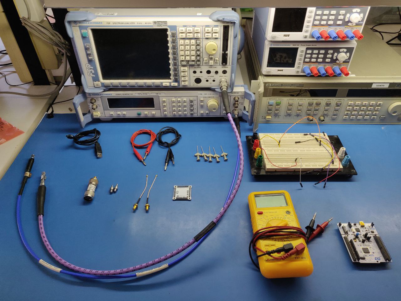
For performing this test, the following items are required:
- 1 completely soldered P/L2 board.
- 1 breadboard
- 2 male to male jumper cables
- 5 male to female jumper cables
- 5 handsfree oscillocope probe
- 2 banana-banana power cables
- 1 multimeter with sharp termination cables
- 1 power supply
- 1 Signal generator (10 MHz - 3 GHz)
- 1 Spectrum Analyser (up to 3 GHz)
- 1 SMA DC block
- 2 SMA to SMA 50 ohm coaxial cables
- 2 SMA to U.FL header transition
- 2 SMA to MS156 probe transition
- 1 OBC board with at least the STM and pull up resistors soldered OR a Nucleo board + PC with SMT32Cube IDE + USB to mini USB cable
In what follows the pinout of the P/L2 board will be explained. It is worth mentioning that the vertical pinout is shared by all boards of the PQ, so in case an OBC board is used, the connection can easily be done by simply mounting the 2 PCBs together using the vertical connectors. The pins used for this test are the folowing:
| Connector index | Pin position | Name | Description |
|---|---|---|---|
| J1 | 1 | SDA1 | I2C data bus 1 (reserved for payloads) |
| J1 | 2 | SCL1 | I2C clock bus 1 (reserved for payloads) |
| J1 | 9 | GND | Global Ground pin |
| J1 | 10 | VCC | Global supply line (3.3V but not for P/L2) |
| J2 | 7 | GND | Global Ground pin |
| J2 | 10 | GND | Global Ground pin |
| J3 | 2 | PH6 | +Y photodiode pin (post amplification) |
| J3 | 6 | P/L_Power | PoL - controlled supply line (3.1 V) |
| J4 | 8 | DAC | OBC STM32 Digital-to-Analog output pin |
| J4 | 9 | ADC | OBC STM32 Analog-to-Digital input pin |
They can be located as follows in the vertical top (left) & bottom (right) views shown below:

Next up, the steps for the connections will be presented. They need to be replicated whenever a new test sub-section is performed, unless stated otherwise.
- Mount the OBC&COMMS and P/L2 board together using the vertical connectors. Make sure that both of them match the rotation configuration.
A light mounting is recommended as not to fully latch the pins which will make subsequent separation of the boards difficult. If however, for any reason, vertical mounting is not feasible OR if a Nucleo Board is chosen to be used instead of the OBC&COMMS board, then the connection of all pins shown above except VCC and GND should be done with male-female jumper cables, using oscilloscope probe endings to better latch to the P/L2 male vertical pins.
-
Power on the power supply with the OUTPUT DISABLED and set it to 3.3 V with a current limit of 500 mA, connecting it using the banana connectors to the breadboard.
-
Using 2 jumper cables of preferably distinctive colours (red for supply and black for GND), connect the breadboard GND to any of the GND pins shown in the pinout above, and the breadboard supply to the VCC pin. The reader should also use this opportunity to understand how the powering of this payload is done.
As the payloads are duty-cycled consumers whose activation needs to be strictly controlled, their supply is done through a PoL (point of load) switch located on the OBC board that, upon activation with a GPIO (General purpose Input/Output) pin of the STM32, enables the 3.3V permanent voltage line of the PocketQube to supply the P/L board through the P/L_Power pin. As a result, during this test, as this SSV aims at testing the payload under the same conditions as those encountered in orbit, the powering has been chosen to be done the nominal way, from the 3.3V VCC all the way through the OBC-controlled Pol, through the P/L_Power pin and into the actual payload board. It warrants mentioning however that, if someone would like to test exclusively the P/L2 board OR if the Nucleo Board approach has been chosen, direct powering through the P/L_Power pin is possible (in which case the power supply is directly connected to the latter pin, with the VCC pin not seeing use).
-
Power on the signal generator with the OUTPUT DISABLED and carefuly connect the 50 ohm SMA-SMA coaxial cable to its output. Attach the SMA to U.FL adaptation to the other end.
-
Power on the spectrum analyser and very carefully attach a DC block directly to its input. Then connect to the free end of the DC block a SMA-SMA 50 ohm coaxial cable. Do not attach any of the remaining U.FL or MS-156 adaptations yet, as the type needed depends on the sampling point.
-
Enable the power supply output and verify that the SMT32 is correctly powering on and that the latest version of the P/L2 task software is flashed.
For details on STM32 operation, please refer to the OBC page within ³Cat-NXT Design chapter. Before continuing from this point, the reader should be able to operate the STM at least in what regards the I2C bus, ADC input and DAC output, as well as flash the newest version of the software.
After a test session is completed, regardless of the length of the hiatus, one should proceed to disable the signal generator and power supply (in this order), disconnect all the cables (very gently in the case of the U.FL and MS156 terminations), power off all equipment and safely store all cables in their designated bags, terminations apart, and place the item under test in an antistatic bag equipped with a silica bag.
Pass/Fail Criteria
This test will be considered passed if all of the following actions are performed succesfully:
- The code executes correctly upon flashing.
- A 2 GHz band noise-level sweep centered at 1.5 GHz is correctly filtered, amplified, downconverted to 70 Mhz within a 4 MHz bandwidth.
- The resulted signal is translated by the RSSI into the appropiate voltage according to the manufacturer's specifications.
- The data aquisition process is correctly performed with the data being accessible from the STM32's flash memory banks.
Test Plan (By Subblocks)
Before moving towards the testing of the whole subsystem, in order to single out possible errors, the payload's isolated segments will be tested a part, starting for simplicity with those which do not require a STM32 (be it a Nucleo Board or the OBC&COMMS board) to be verified.
5V booster
The 5V booster, in the form of LT3048, is needed to augument the line voltage of 3.3 V of the PocketQube to 5 V in order to correctly supply the LEE2-6+ LNA. The testing procedure for it is listed below:
-
Ensuring that the correct connections have been done as per the Test Set-Up section above, enable the output of the power supply.
-
If the OBC&COMMS board approach has been chosen, also activate the P/L2 PoL via the IDE used to debug the task software. If feeding the board directly through the P/L_Power pin, then skip this step.
-
Check the current drain of the power supply. It should be around the value of XXX mA.
-
Using the multimeter set in voltage mode, measure the voltage between the P/L_Power pin and GND. It needs to be between 3.3 V and 3.1 V.
-
With a sharp multimeter termination, as looking at the BOT side of the board, gently sample the left terminal of the R1 resistor and GND. The value should be about 5 V. If it is the case, it can be concluded that the booster works properly.
RF chain Low Noise Amplifier (LNA)
In the form of the LEE2-6+, fully explained in the appropiate P/L page, under the ³Cat-NXT Design chapter, the LNA is supposed to provide a gain between 20.6 dB (at 1 GHz) and 18.9 dB (at 2 GHz) over the L-band. To test this feature, a signal will be introduced at the receiver's input, and sampled from the first RF chain probe. The procedure is as follows:
-
Not having modified the configuration done in the 5V booster subsection, the board should be operational. This can be checked by having a current consumption of cca xxx mA seen on the power supply display and with a voltage between 3.1 V and 3.3 V measured between the P/L_Power and GND pins. If otherwise, repeat the previous sub-section steps.
-
Connect the signal generator output through the SMA-U.FL termination to the J5 coaxial header located on TOP side of the board, lower right corner.
-
Attach a SMA-MS156 probe termination to the free end of the coaxial cable of the spectrum analyser and connect it to the J6 MS156 probe header found on the BOT side of the board, on the left hand side.
The MS156 probes act like an electrically closed circuit when in nominal state, but disconnect the subsequent circuit when probed. This means that probing cuts elements further on the transmission line from the input, in this case anything past the J6 probe: bandpass filter, tuner, IF chain, etc...
-
Set up the spectrum analyser to a center frequency of 1.5 GHz, a span of 2 GHz (having a total observable window from 500 MHz to 2500 MHz) and using the maxim Autopick setting for ease of interpretation.
-
With the board and LNA powered as detailed above, select a tone of -50 dBm in ampltude and 1 GHz of frequency on the signal generator and then enable its output.
-
Observe the reading on the spectrum analyser. The same tone inputted should be visible, but with an amplitude gain of cca 20 dB. Note down any frequency shift if the case and take screen captures as needed.
-
Repeat the last two steps, this time at a number of different frequencies from 1 GHz to 2 GHz. It is recommended to do so at 200 MHz apart.
-
If the gain observed along said measurements coincides with the values provided by the manufacturer within a 5% tolerance, this test is considered passed. Note that the values of gain according to the datasheet are: 20.6 dB (1 GHz), 20.3 dB (1.2 GHz), 19.9 dB (1.4 GHz), 19.6 dB (1.6 GHz), 19.3 db (1.8 GHz) and 18.9 dB (2 GHz).
Bandpass filter
The BFCG162W bandpass filter's function is to preselect the signal within a range indicated by the manufacturer to be between 950 MHz and 2200 MHz, with an insertion loss of lower than 3 dB in-band and higher than 20 dB out-of-band. These characteristics can be tested as follows:
-
With the configuration from the Set-Up section in place as well as the OBC PoL turned on, connect the SMA-MS156 ended cable of the spectrum analyser to the J7 MS156 probe header found on the BOT side of the board. Make sure that the previous connection to J6 done in the previous sub-section using the MS156 is removed, in order to return the probe header to its electrically closed morphology.
-
Make sure the output of the signal generator is still connected through the J5 U.FL coaxial header on the TOP side of the board
-
Set up the spectrum analyser to a center frequency of 1.5 GHz, a span of 2 GHz (having a total observable window from 500 MHz to 2500 MHz) and using the maxim Autopick setting for ease of interpretation.
-
Configure the signal generator to output a 500 MHz - 2500 MHz frequency sweep of -50 dBm amplitude and enable its output.
-
Observe the resulting signal on the spectrum analyser. The frequency components outside of the 950 MHz - 2200 MHz range should show an attenuation of at least 20 dB, with the in-band components not decreasing more than 3 dB. If the previous statements are empirically proven true, then it can be concluded that the bandpass filter is operational.
Downconversion tuner
The downconversion of this receiver is done using the I2C controlled MAX2121 VSSAT tuner, from the 1-2 GHz RF chain to the 70 MHz IF chain, by applying a frequency sweep. Worth mentioning is that the task software verification is only subject to verification in the functional sense in this test, and it is explained in detail in ... Additionally, it is the last item of this receiver's front end to allow separate verification of sorts, as the subsequent IF chain is a differential line with no probing point, followed by the adaptation network of the RSSI and the RSSI itself. Therefore, the steps to follow are:
-
Make sure that the configuration from the Set-Up section is in place.
-
Verify that the OBC PoL is turned on and the DAC pin holds a voltage of 2.7 V.
-
Leave the signal generator unconnected and its output disabled. Remove any MS156 probe termination that might have remained attached from previous tests.
-
Attach a SMA-U.FL probe termination to the free end of the coaxial cable of the spectrum analyser and connect it to the J8 U.FL coaxial header found on the BOT side of the board, in the central region of the PCB.
-
Set up the spectrum analyser to a center frequency of 1.5 GHz, a span of 2 GHz (having a total observable window from 500 MHz to 2500 MHz) and using the maxim Autopick setting for ease of interpretation.
-
By using the IDE, set the downconversion tuner's local oscillator frequency between 930 MHz and 1930 MHz with steps of 50 MHz.
-
On the spectrum analyser's display, deltas of frequencies corresponding to those set in the software should appear. Note down any frequency shift. If the frequencies match with a 5 MHz tolerance, the isolated testing of the downconversion tuner is concluded with success.
Photodiode Opamp
-
Make sure that the configuration from the Set-Up section is in place as well as the OBC PoL is turned on.
-
Orient the board towards a sufficiently luminous source and sample the voltage at the terminals of the photodiode. Write the value down. It should be small (micro or nano volts) but non null and varying with the degree of luminosity.
-
Using a sharp termination multimeter and without moving the board any longer (as not to change luminous conditions), sample the voltage this time between the PH6 and GND pins. Write down the value. Ihe value should be cca 20 times bigger. If the case, then it can be concluded that the photodiode and its opamp block are operating as expected.
Test Plan (Full subsystem)
From this point the document is a stub.
Having tested and isolated possible errors as much as possible in a bit-by-bit manner in the previous section, a full subsystem test will now be performed.
-
Make sure that the configuration from the Set-Up section is in place as well as the OBC PoL is turned on.
-
Connect the signal generator output through the SMA-U.FL termination to the J5 coaxial header located on TOP side of the board, lower right corner. It is recommended that at least the first full SSV is done by way of signal generator input, with later tests possibly replacing this input with the real one by way of the antenna in order to firstly test the front end separate from any possible errors.
-
Configure the signal generator to output a 500 MHz - 2500 MHz frequency sweep of -100 dBm amplitude with random spikes at -80 dBm and enable its output.
-
Using the IDE, initiate the P/L task within the STM32, using the full PQ firmware scheduler.
-
Using the Umbilical connection, download the flash memory experiment files.
Test Results
Description of the Test results (photos, tables, etc) with interpretation.
5V booster test:
RF chain LNA test:
Bandpass filter:
Downconversion tuner:
Photodiode Opamp:
Full subsystem test:
Anomalies
List of deviations to the Test Specification and Procedure and non-conformances witnessed during the test campaign, including a brief description, the close-out status and reference to the relevant reports.
Conclusions
Verified requirements (and within which part of the test), close-out judgement (compliance status) and rationale, statement of open issues and possible remediating actions