ᴾᵒCat: RFI L-Band Payload
In this book information about ᴾᵒCat-2 P/L , a RFI Monitoring payload at the L-Band, is found including a subsystem description hardware and software designs as well subsystem verification.
Hardware Design
Document scope
This document aims to describe the design process and considerations involved in the designing a L-band Radio Frequency Interference (RFI) payload with the purpose of monitoring and mapping the Electromagnetic Interference (EMI) coming from the Earth in the 1 ↔ 2 GHz range in an effort of researching if emergent telecommunication services in this band can be interfering with the GNSS systems and the 1400 ↔ 1427 MHz band reserved for microwave radiometry. This monitoring receiver consists of 2 main elements: a receiver front-end equipped with a power detector and a deployable antenna.
Front end design
Basic architecture
The architecture will be that of a basic, homodyne receiver. The Radio Frequency (RF) input is amplified using a Low Noise Amplifier (LNA), preselected using a cca 1-2 GHz band pass filter and then fed into a controllable frequency tuner, which downconverts the input into near baseband intermediate frequency (IF) for processing. The resulting signal is then filtered using very high Q, low bandpass filter, centred at the desired IF for tune filtering, and passed to a Radio Signal Strength Indicator (RSSI) Integrated Circuit (IC) to sample the spectral element's power and direct the data to the On Board Computer's (OBC) Analog to Digital Converter (ADC) input.

Functional schematic and IC choice
In order to translate the abstract choice of architecture into a functional schematic, components are required that fit the rather strict requirements explained previously. With the ongoing global semiconductor shortage, and the small satellite industry increasing its dependancy on Components Off The Shelf (COTS), the design choices from this point onwards have been heavily influenced by the distributors' availability and stock.
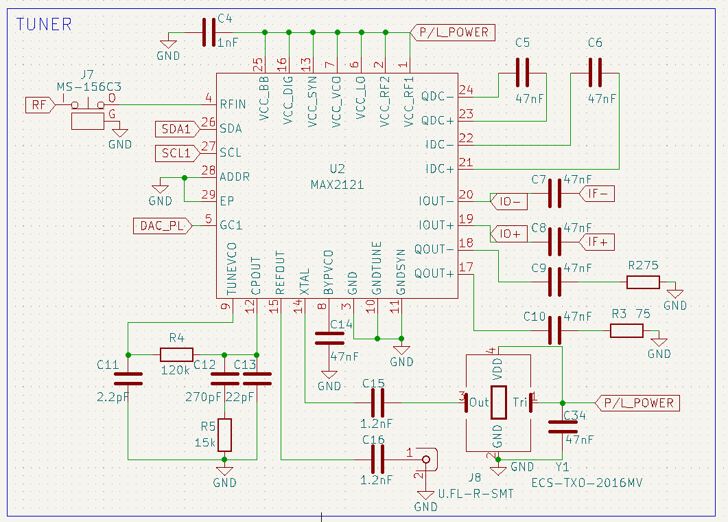
To kick off, the most restrictive element, in terms of the aformentioned limited availability, will be discussed: the downconversion tuner. It is worth mentioning that initial designs envisioned a simple passive mixer with a standard Local Oscillator (LO) in the form of a wideband Voltage Controlled Oscillator (VCO) controlled by the OBC's Digital to Analog Converter (DAC) output. However, due to image frequency issues inherent to such superheterodyne architectures, as well as the continuous dwindle of adequate VCO and IF filter pairs, this simplistic design has been forcefully discarded. The current iteration is therefore based on MAX2121 direct-conversion L-Band Tuner IC originally used for Television through Satellite (TVSAT) applications. The chip sports 24 I2C controllable monolithic VCOs, a complete fractional-N Phase Locked Loop (PLL) circuit covering the 925 ↔ 2175 MHz frequency range, internally adjustable amplifiers offering up to 80 dB of gain, active mixers which eliminate the image frequency issues, double differential output for both I and Q modulation elements, and integrated 123 MHz IF output low pass filters, all on a minute 5 mm X 5 mm, 28 pin TQFN package. In terms of disadvantages, one could point out the high power consumption of cca 150 mA at 3.3 V line voltage, a 75 Ω matched input and output lines, as well as a staggering Noise Figure (NF) between 8 and 12 dB, depending on the amount of ajustable gain desired. While these weak points are all valid sources of concern and are addressed in the following component descriptions, a mention should go to the termination impedance. As the chip has been designed for TVSAT applications that have since seen less and less usage, the 75 Ω specific impedance is introducing issues in finding matched LNAs and Filters in the COTS market, with the few options still existing either not being wideband enough, having too high a consumption or centered in other frequency bands, as most of the industry has moved to 50 Ω terminations, resulting in opting for components of the latter impedance with the possibility of introducing a matching network. As the reader can already begin to observe, the design choices are intricate and bidirectional, with cascading changes affecting all component choices.
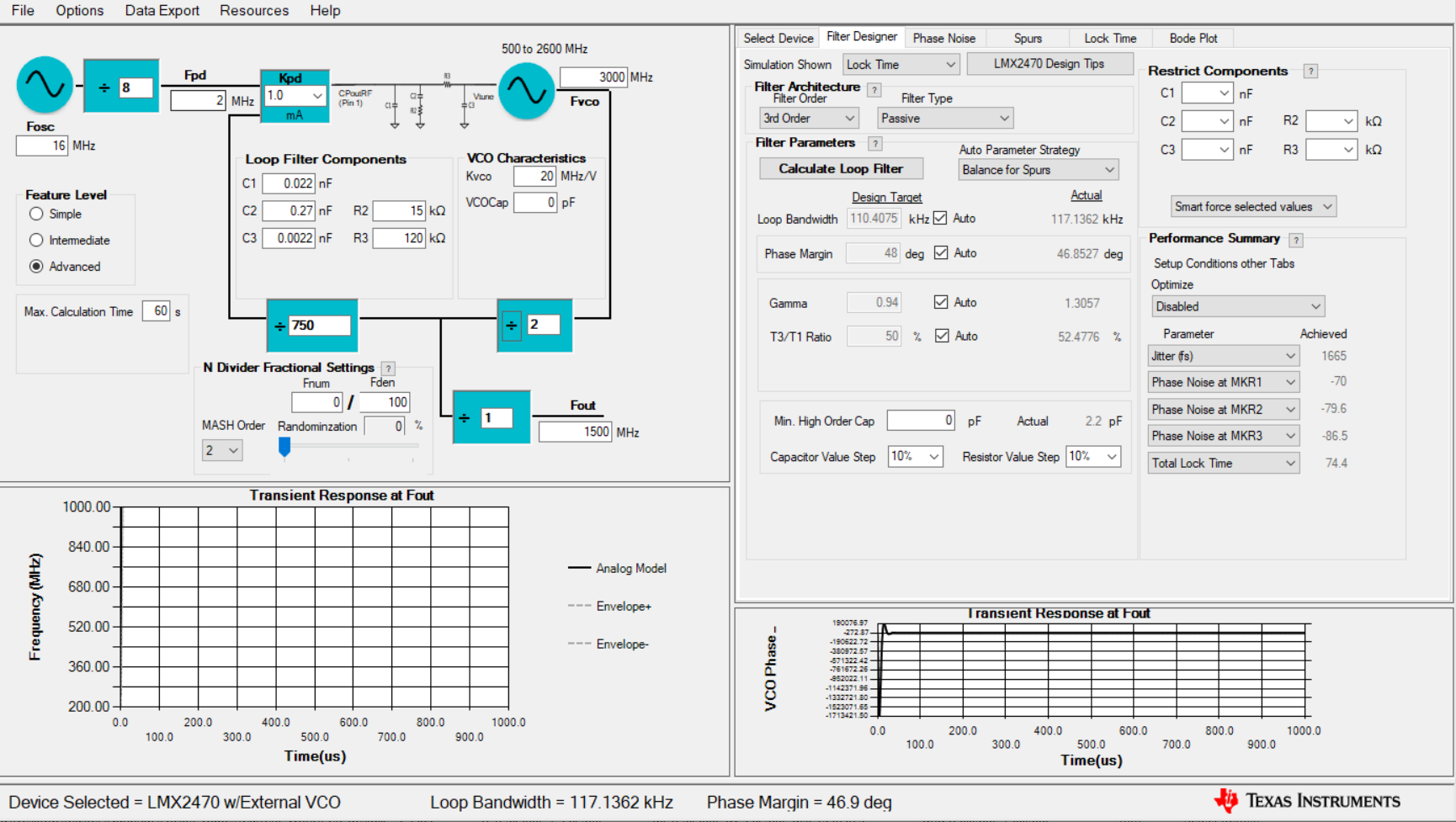
In terms of biasing, the MAX2121's integrated N-fractional PLL most notably requires a reference frequency provided by means of a discrete crystal oscillator, with the value being chosen as a tradeoff between on one side the maximum Equivalent Series Resistance (ESR) and spectral resolution obtained at the front end output to a commonly-found value of 16 MHz. Additionally, while the feedback divider in the form of the Synthesizer block is itself incorporated within the chip, for achieving control, an external control loop is required between the output of the charge pump (CPOUT) and the VCO tuning (TUNEVCO) pins. The 3'rd order filter configuration shown below has been obtained as a result of a software-assisted analysis using Texas Instruments' PLLatinumSIM simulation tool, optimising for stability and locking time of less than 50 us, allowing for a sweeping step of 2 MHz, when operating the tuner by writing in the N-Divider, F-Divider, R-Divider registers 1,2,3,4,6 and 7 of the chip's internal memory bank.
Lastly, an array of filtering and DC-blocking capacitors have been added to multiple pins as per the manufacturer's instructions.
Before continuing, it is worth discussing the previously mentioned possibility of introducing an adaptation network at the input of the tuner to convert the 50 Ω of the preceding elements to the 75 Ω of the MAX2121. Considering both that the RF chain covers a very wide band (from 1 to 2 GHz), and the PocketQube's strict power and space limitations, the solution considered was a L-pad resistive network made with two broadband SMD resistors of 43 and 91 Ω respectively, trading approximatively 5.6 dB loss for the simplicity and broadband nature.
On the other hand, in the event in which the choice is made not to implement this adaptation network, considering the signal level at the input of the tuner being cca -86 dBm, a transition from the 50 Ω to 75 Ω specific impedance will imply a reflection coefficient of 7 dB, which, considering also the band pass filter insertion loss of 3 dB and the LNA's isolation of 22.5 dB, will translate into a back-radiated signal at the antenna of cca -118.5 dBm, significantly lower than the computed noise floor of -105 dBm, with no chance of harming the intermediate components. In light of this, the choice of adding said adaptation network has been discarded.
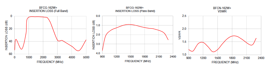
Moving back the RF chain, the preselection filter has been choosen in the form of the 950 ↔ 2200 MHz BFCG-162W+ ceramic bandpass filter. Its desirability originates from its extremely wide passband, minute size (2 x 1.25 mm equivalent to 0805 imperial casing), LTCC construction and very good stability with temperature, combined with -55C ↔ 125C operating range. One downside could be the fact that its band doesn't perfectly match the 1 ↔ 2 GHz RF input specified by the requirements. This is not a critical aspect however, as the final reading can be controlled from the OBC sweep, and the extra tail-ends are not significant. Moreover, the stop band insertion loss of upwards of 40 dBs ensures no undesired spectral elements outside of the band would interfere with the payload input, at the cost of cca 3 dB of pass band insertion losses.
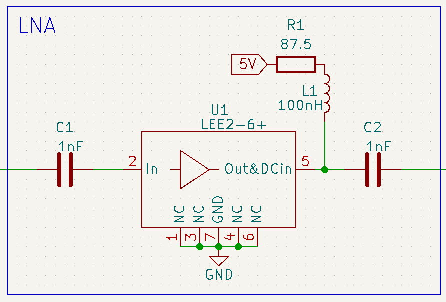
Next up, while the gain of the previously presented tuner is itself more than enough to bring any incoming signal from the noise floor of cca -105 dBm (please refer to the IF filter description below) to the -77 ↔ 9 dBm sensitivity range of the RSSI (please check the Gain Budget section below), the tuner's noise figure of 8 dB (at minimum gain) will decrease the performance of the receiver substantially. To this end, the LEE2-6+ LNA has been placed at the start of the RF chain to provide a 21-19 dB preamplification along the whole L-band, with a very low power consumption of 16 mA at 5 V. This way, this chip's better NF of 2.3 dB (at 2 GHz), when placed before the tuner, will, alongside with the insertion loss of the Preselection Filter that follows, heavily improve the receiver's overall NF:


In terms of circuit biasing, the IC is attacked in current, with nominal operation being obtained when supplied 16 mA at 3.6 V. To this end, a SMD resistor has been chosen to bridge the 1.4 V drop as a current source of the required amperage, resulting by Ohm's law in a 87.5 Ω value.The only other required components are two DC-block capacitors for both the input and output of the IC, as well as a RF choke for the supply. The values of these components are frequency dependant and are computed for each chain: for the inductors, their self resonant frequency must be considerably higher than the working frequency: 100 nH and 3.3 uH for the RF, while the capacitors being chosen so their cuttoff (-3dB) frequency lower than the working frequency: 10 nF for the former link, and 1 nF for the latter.
Furthermore, following the tuner, the 5'th order shunt first Chebyshev band pass filter centered at 70 MHz shown below has been implemented, sporting a 4 MHz narrow bandwidth, negligible insertion loss and 0.1 dB passband ripple. The choice of the central frequency has been made as result of filter optimisation, upper limit of the tuner's integrated Low Pass Filters (LPF), combined with distancing from the very low frequencies in order to avoid coupling with any Pulse Width Modulation (PWM) elements introduced with voltage boosters and other switching regulators used within the satellite.

The purpose of this added filter is to provide a good element isolation with its narrow band and high isolation, resulting in an system spectral resolution of 4 MHz, after the sampling. Additionally, as both the tuner output and RSSI input are differential, the filter has been implemented likewise, complete with 75 Ω matching complying with the MAX2121 integrated terminations. Thus, the IF chain enjoys reduced electromagnetic interference (EMI) production, reduced sensitivity to induced or coupled noise, less distortion of edges due to signal reflections.

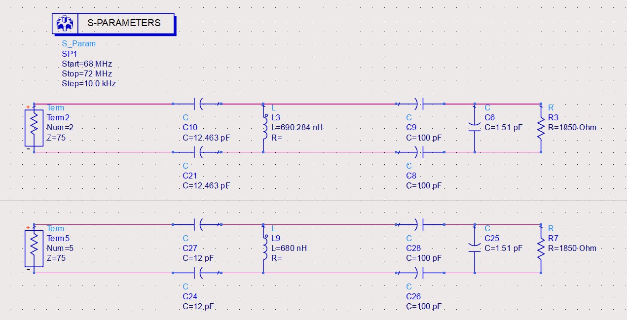
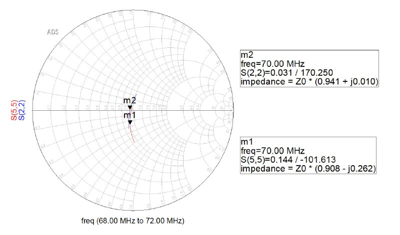
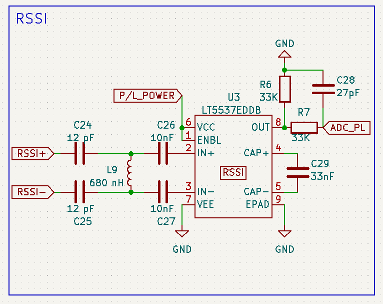
Next up, The RSSI detector upon which the payload is based is Linear Technology Corporation's LT5537 chip. This chip provides a log-linear output response that depends on the RF power at its input and is able to measure RF power from 10 MHz to 1000 MHz, with the input being set by the previous filter to 70 MHz. At this frequency, the RSSI detector has a single ended sensitivity of -77 dBm with the advantage that, by using the high impedance differential input adapted using a matching network from the 75 Ω characteristic impedance of the the previous elements to the 1.85 kΩ & 1.51 pF equivalent parallel RC of the RSSI as per the manufacturer's specifications, the sensitivity can be further improved to values as low as -82 dBm at the working frequency. The matching network is a simple LC configuration and has been obtained using the Keysight Advanced Design Software (ADS), with the results displayed below corresponding to their theoretical and real market component values:
Additionally, by using DC blocking capacitors at the input, along with a 33 uF capacitor in the external feedback loop, a phase margin of 84 degrees has been achieved, resulting in increased stability, with the load resistor of 33 kΩ providing an output log-linear rate of 20 mV/dB. Lastly, a simple low pass filter has been added at the output to allow the ADC sampling frequency to comply with the Nyquist limit. What this means is that, due to the ADC's limitation of maximum sampling frequency, the signal it receives needs to be limited to a maximum bandwidth that the LPF limits. This however introduces the issue that, while fully capable to detect slowly changing input power, some high spectral elements (sudden changes in time) will not be detected, with this problem being accepted as a design limitation. Considering the most permissive and restrictive of sampling rates of the STM32L476:

The fully biased configuration is thus showed below:
In what follows, the gain budget will be analysed.

Considering an overall receiver bandwidth of 4 MHz (as given by the most restrictive filter), a ground noise temperature of 290 K and the equivalent Noise Figure obtained previously in the LNA section of 2.61 dB, one can obtain the background noise level of -105 dBm at the antenna input. As a result of this, along with the total front end gain, the RSSI input power can be obtained as being approximatively -11.5 dBm, falling well into its sensitivity range. By correlating this level with the Input Power - Output Voltage characteristics provided by the manufacturer, the reader can notice that the front end chain amplification is more than sufficient to allow low power signal acquisiton. On the other hand, the maximum input power the RSSI can register is 9 dBm, allowing for reception of high power signals up to -84.5 dBm (sensed at the antenna output), resulting in a dynamic range of 20.5 dBs. In the light of this, one argument could be made that, if one was to proceed with the inclusion of the 50 Ω to 75 Ω matching network and thus decreasing the FE gain, the overall receiver dynamic range would be increased to 29.5 dB. At this stage of the design process, it has been decided that such a gain would not be worth it.
Moreover, within the -60 ↔ 10 dBm range of Input Power, provided it is used at positive temperatures, the RSSI Output Voltage graph follows a cvasi-linear figure, which is empirically deduced in the ³Cat-NXT Integration and testing book, under the appropriate Functional tests page.
Additionally, in order to supply the LNAs, a 5V boost converter in the form of LT3048-5 has been used, with the biasing elements respecting the manufacturer's specifications.
Finally, as the current design iteration envisions a stowable broaband helical antenna (more on that on the appropiate section below), after its deployment, the payload board will be the de-facto top board of the PocketQube. In accordance with the requirements regarding the Sensor Module of the Attitude Determination and Control System (ADCS), and more specifically with the need of photodiodes on all sides of the cube, one such device has been installed on this payload's board upper face in the form of SLCD-61N8. However, as this photodiode's output signal is very small (cca 170 uA) and its connection does not follow the usual path through the Breakout Board, where a series of Operational Amplifiers (Opamps) have been used to amplify this signal to bring it within the sensibility of the OBC's ADC, one such device was employed, in the form of LT071DBV, biased in order to match the amplification factor of the other Opamps in order to avoid sensor data misscalibration, with the resulting signal being routed through the multifunctional STM_PB0 pin.
To conclude this section, the complete schematic can be consulted below:
Printed circuit board design
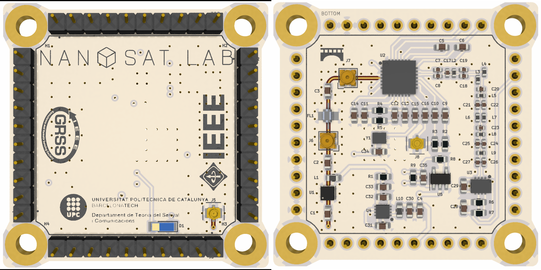
To begin, as this Payload's Printed Circuit Board (PCB) will be part of the PocketQube's central PCB stack, it needs to comply with said standard, presented below, having fixed the outline, dimensions and locations of both the 4 screws and vertical connectors. In terms of connectors, the SLW-110-01 has been replaced with the far slimmer BBL-110 as there is not other upper PCB to be connected, and only the inferior set of pins are needed to complete the vertical connection to the OBC&COMMS board beneath.
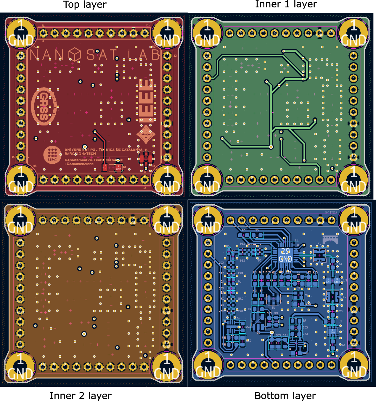
Next up, a big design factor consists in the helical antenna high space occupancy (current design iteration involves a 34 mm diameter coil being stowed and deployed from above the PCB) which resulted in the decision being made to place the entirety of the front end elements on the bottom layer, with the exception of the photodiode because of reasons explained previously as well as the C.FL-R-SMT-1 coaxial connector, with the resulting blank top layer acting as a 40 x 40 mm ground plane for the antenna. Additionally, as this board will be exposed to sunlight after the antenna deployment, in accordance with the thermal analysis, the soldermask color has been set to white. Furthermore, as the Coplanar Waveguides have been used for the RF Transmission Lines (TL), and they require by definition a ground plane underneath the trace, another of the former has been added just above the bottom layer (as seen from the nominal PQ positioning), thus creating the need for inner layers. Moreover, as the number of fabricable inner layers tends to be imposed by manufacturers to be even, an additional layer has been employed between the top layer and the ground plane layer for the bottom layer, which has been used for power lines and analog small signal routing. The final stack-up can be seen below.

Before diving into the bottom layer implementation, a study has been performed both using KiCad's integrated calculator, as well as Saturn PCB Design Toolkit in order to obtain the required dimensions for traces and vias corresponding to the characteristic impedances of 50 Ω for the RF chain and 75 Ω for the RF chain respectively, with the results being shown in the table below. Additionally, the detailed simultaion snippets are attached to this page.

Starting with the RF chain, as can be seen in the left part of the broken down picture of the board below, it presents a standard TL structure, with components being placed in a straight line, surrounded by a RF via fencing, and with the solder mask removed, in order to reduce losses and preserve the characteristic impedance. Also, as the chain is comparable to the length of the PCB, it has been reoriented using a circular 90 degrees bend to minimise reflections.
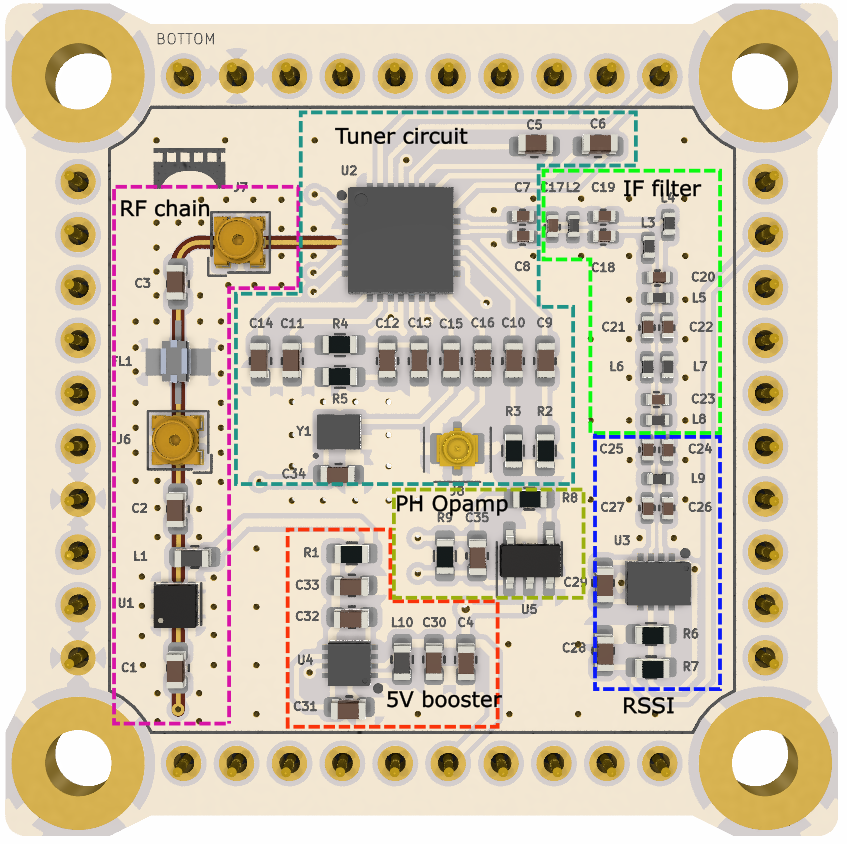
Now would be an adequate time to raise the reader's attention to the MS-156C3 Hirose probe headers (J6 and J7) present both before the bandpass filter and before the tuner. They consists of an internally matched 50 Ω coaxial termination, fit for same family SMA conversion adapters, allowing for easy on-board testing of the TL. Worth mentioning is that, when introducing the probe in the header, a mechanical switch is activated, the input of the switch being connected to the probe input, while disconnecting the output of the header, thus rendering the effect of the rest of the front end moot. This way of operation allows for one way testing, thus reducing the number of effects that can affect a measurement and isolating possible error factors.
Next up, the MAX2121 tuner's biasing has been done by having the filtering and DC-blocking capacitors, as well as the Loop filter and crystal oscillator as close as possible to their respective pins while not affecting the TLs. Noteworthy in this part is that the crystal oscillator working at 16 MHz has been placed within a via guard ring in order to minimise cross-talk, and the addition of a C.FL-R-SMT-1 coaxial header connected which allows access to the tuner's inner synthetising frequency for testing purposes.
Subsequently, the IF 5'th order Chebyshev filter is linked to the tuner's I component differential output. As presented in the Schematic section, it is a differentially matched to 75 Ω bandpass filter made with discrete components and surounded again by via RF fencing. To this end, the major design factor was to achieve a balance between component size and track width, as the further apart the pads, the wider the differential track would need to split to connect to them, and the higher the divagation from the required separation obtained previously in the characteristic impedance study. Conversely, the smaller the components, the higher would be the losses, especially in the case of capacitors. However, in the end, as the monolithic series-parallel structure of the filter, combined with the RSSI adaptation network, initially 0604 imperial along with all other biasing elements of the board, exceeded the PCB available space, the decision was made to both reduce the components size to 0402 imperial, as well as to bend the TL taking advantage of the passive components of the filter, action made possible by the low operation frequency of the IF chain.
Moving to the RSSI, as mentioned previously, its impedance adaptation network has been structurally integrated within the differential monolith, taking advantage of the identical component format, as well as the straight line formation. Additionally, in terms of biasing elements, the load resistor, as well as the ADC's low pass filter have placed as close as possible in order to better compact the structure, thematic that was employed with all this board's modules
Lastly, the 5V booster and the photodiode opamp have been designed according to the manufacturer's layout recommendations and placed as possible to their deserving elements: the RF chain LNA and the photodiode respectively.
Finally, the PCB layer views can be revised below, along with some renders of the final assembly:

Antenna design
Problem formulation
Preliminary solutions
Broadband helical antenna
include simulations CST and VNA results here.
Stowing & Deployment system
Hardware Design L-Band
Document scope
This document aims to describe the design process and considerations involved in the designing a L-band Radio Frequency Interference (RFI) payload with the purpose of monitoring and mapping the Electromagnetic Interference (EMI) coming from the Earth in the 1 ↔ 2 GHz range in an effort of researching if emergent telecommunication services in this band can be interfering with the GNSS systems and the 1400 ↔ 1427 MHz band reserved for microwave radiometry. This monitoring receiver consists of 2 main elements: a receiver front-end equipped with a power detector and a deployable antenna.
Front end design
Basic architecture
The architecture will be that of a basic, homodyne receiver. The Radio Frequency (RF) input is amplified using a Low Noise Amplifier (LNA), preselected using a cca 1-2 GHz band pass filter and then fed into a controllable frequency tuner, which downconverts the input into near baseband intermediate frequency (IF) for processing. The resulting signal is then filtered using very high Q, low bandpass filter, centred at the desired IF for tune filtering, and passed to a Radio Signal Strength Indicator (RSSI) Integrated Circuit (IC) to sample the spectral element's power and direct the data to the On Board Computer's (OBC) Analog to Digital Converter (ADC) input.
Functional schematic and IC choice
In order to translate the abstract choice of architecture into a functional schematic, components are required that fit the rather strict requirements explained previously. With the ongoing global semiconductor shortage, and the small satellite industry increasing its dependancy on Components Off The Shelf (COTS), the design choices from this point onwards have been heavily influenced by the distributors' availability and stock.
To kick off, the most restrictive element, in terms of the aformentioned limited availability, will be discussed: the downconversion tuner. It is worth mentioning that initial designs envisioned a simple passive mixer with a standard Local Oscillator (LO) in the form of a wideband Voltage Controlled Oscillator (VCO) controlled by the OBC's Digital to Analog Converter (DAC) output. However, due to image frequency issues inherent to such superheterodyne architectures, as well as the continuous dwindle of adequate VCO and IF filter pairs, this simplistic design has been forcefully discarded. The current iteration is therefore based on MAX2121 direct-conversion L-Band Tuner IC originally used for Television through Satellite (TVSAT) applications. The chip sports 24 I2C controllable monolithic VCOs, a complete fractional-N Phase Locked Loop (PLL) circuit covering the 925 ↔ 2175 MHz frequency range, internally adjustable amplifiers offering up to 80 dB of gain, active mixers which eliminate the image frequency issues, double differential output for both I and Q modulation elements, and integrated 123 MHz IF output low pass filters, all on a minute 5 mm X 5 mm, 28 pin TQFN package. In terms of disadvantages, one could point out the high power consumption of cca 150 mA at 3.3 V line voltage, a 75 Ω matched input and output lines, as well as a staggering Noise Figure (NF) between 8 and 12 dB, depending on the amount of ajustable gain desired. While these weak points are all valid sources of concern and are addressed in the following component descriptions, a mention should go to the termination impedance. As the chip has been designed for TVSAT applications that have since seen less and less usage, the 75 Ω specific impedance is introducing issues in finding matched LNAs and Filters in the COTS market, with the few options still existing either not being wideband enough, having too high a consumption or centered in other frequency bands, as most of the industry has moved to 50 Ω terminations, resulting in opting for components of the latter impedance with the possibility of introducing a matching network. As the reader can already begin to observe, the design choices are intricate and bidirectional, with cascading changes affecting all component choices.
In terms of biasing, the MAX2121's integrated N-fractional PLL most notably requires a reference frequency provided by means of a discrete crystal oscillator, with the value being chosen as a tradeoff between on one side the maximum Equivalent Series Resistance (ESR) and spectral resolution obtained at the front end output to a commonly-found value of 16 MHz. Additionally, while the feedback divider in the form of the Synthesizer block is itself incorporated within the chip, for achieving control, an external control loop is required between the output of the charge pump (CPOUT) and the VCO tuning (TUNEVCO) pins. The 3'rd order filter configuration shown below has been obtained as a result of a software-assisted analysis using Texas Instruments' PLLatinumSIM simulation tool, optimising for stability and locking time of less than 50 us, allowing for a sweeping step of 2 MHz, when operating the tuner by writing in the N-Divider, F-Divider, R-Divider registers 1,2,3,4,6 and 7 of the chip's internal memory bank.
Lastly, an array of filtering and DC-blocking capacitors have been added to multiple pins as per the manufacturer's instructions.
Before continuing, it is worth discussing the previously mentioned possibility of introducing an adaptation network at the input of the tuner to convert the 50 Ω of the preceding elements to the 75 Ω of the MAX2121. Considering both that the RF chain covers a very wide band (from 1 to 2 GHz), and the PocketQube's strict power and space limitations, the solution considered was a L-pad resistive network made with two broadband SMD resistors of 43 and 91 Ω respectively, trading approximatively 5.6 dB loss for the simplicity and broadband nature.
On the other hand, in the event in which the choice is made not to implement this adaptation network, considering the signal level at the input of the tuner being cca -86 dBm, a transition from the 50 Ω to 75 Ω specific impedance will imply a reflection coefficient of 7 dB, which, considering also the band pass filter insertion loss of 3 dB and the LNA's isolation of 22.5 dB, will translate into a back-radiated signal at the antenna of cca -118.5 dBm, significantly lower than the computed noise floor of -105 dBm, with no chance of harming the intermediate components. In light of this, the choice of adding said adaptation network has been discarded.
Moving back the RF chain, the preselection filter has been choosen in the form of the 950 ↔ 2200 MHz BFCG-162W+ ceramic bandpass filter. Its desirability originates from its extremely wide passband, minute size (2 x 1.25 mm equivalent to 0805 imperial casing), LTCC construction and very good stability with temperature, combined with -55C ↔ 125C operating range. One downside could be the fact that its band doesn't perfectly match the 1 ↔ 2 GHz RF input specified by the requirements. This is not a critical aspect however, as the final reading can be controlled from the OBC sweep, and the extra tail-ends are not significant. Moreover, the stop band insertion loss of upwards of 40 dBs ensures no undesired spectral elements outside of the band would interfere with the payload input, at the cost of cca 3 dB of pass band insertion losses.
Next up, while the gain of the previously presented tuner is itself more than enough to bring any incoming signal from the noise floor of cca -105 dBm (please refer to the IF filter description below) to the -77 ↔ 9 dBm sensitivity range of the RSSI (please check the Gain Budget section below), the tuner's noise figure of 8 dB (at minimum gain) will decrease the performance of the receiver substantially. To this end, the LEE2-6+ LNA has been placed at the start of the RF chain to provide a 21-19 dB preamplification along the whole L-band, with a very low power consumption of 16 mA at 5 V. This way, this chip's better NF of 2.3 dB (at 2 GHz), when placed before the tuner, will, alongside with the insertion loss of the Preselection Filter that follows, heavily improve the receiver's overall NF:
In terms of circuit biasing, the IC is attacked in current, with nominal operation being obtained when supplied 16 mA at 3.6 V. To this end, a SMD resistor has been chosen to bridge the 1.4 V drop as a current source of the required amperage, resulting by Ohm's law in a 87.5 Ω value.The only other required components are two DC-block capacitors for both the input and output of the IC, as well as a RF choke for the supply. The values of these components are frequency dependant and are computed for each chain: for the inductors, their self resonant frequency must be considerably higher than the working frequency: 100 nH and 3.3 uH for the RF, while the capacitors being chosen so their cuttoff (-3dB) frequency lower than the working frequency: 10 nF for the former link, and 1 nF for the latter.
Furthermore, following the tuner, the 5'th order shunt first Chebyshev band pass filter centered at 70 MHz shown below has been implemented, sporting a 4 MHz narrow bandwidth, negligible insertion loss and 0.1 dB passband ripple. The choice of the central frequency has been made as result of filter optimisation, upper limit of the tuner's integrated Low Pass Filters (LPF), combined with distancing from the very low frequencies in order to avoid coupling with any Pulse Width Modulation (PWM) elements introduced with voltage boosters and other switching regulators used within the satellite.
The purpose of this added filter is to provide a good element isolation with its narrow band and high isolation, resulting in an system spectral resolution of 4 MHz, after the sampling. Additionally, as both the tuner output and RSSI input are differential, the filter has been implemented likewise, complete with 75 Ω matching complying with the MAX2121 integrated terminations. Thus, the IF chain enjoys reduced electromagnetic interference (EMI) production, reduced sensitivity to induced or coupled noise, less distortion of edges due to signal reflections.
Next up, The RSSI detector upon which the payload is based is Linear Technology Corporation's LT5537 chip. This chip provides a log-linear output response that depends on the RF power at its input and is able to measure RF power from 10 MHz to 1000 MHz, with the input being set by the previous filter to 70 MHz. At this frequency, the RSSI detector has a single ended sensitivity of -77 dBm with the advantage that, by using the high impedance differential input adapted using a matching network from the 75 Ω characteristic impedance of the the previous elements to the 1.85 kΩ & 1.51 pF equivalent parallel RC of the RSSI as per the manufacturer's specifications, the sensitivity can be further improved to values as low as -82 dBm at the working frequency. The matching network is a simple LC configuration and has been obtained using the Keysight Advanced Design Software (ADS), with the results displayed below corresponding to their theoretical and real market component values:
Additionally, by using DC blocking capacitors at the input, along with a 33 uF capacitor in the external feedback loop, a phase margin of 84 degrees has been achieved, resulting in increased stability, with the load resistor of 33 kΩ providing an output log-linear rate of 20 mV/dB. Lastly, a simple low pass filter has been added at the output to allow the ADC sampling frequency to comply with the Nyquist limit. What this means is that, due to the ADC's limitation of maximum sampling frequency, the signal it receives needs to be limited to a maximum bandwidth that the LPF limits. This however introduces the issue that, while fully capable to detect slowly changing input power, some high spectral elements (sudden changes in time) will not be detected, with this problem being accepted as a design limitation. Considering the most permissive and restrictive of sampling rates of the STM32L476:
The fully biased configuration is thus showed below:
In what follows, the gain budget will be analysed.
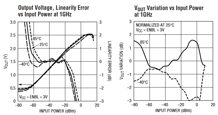
Considering an overall receiver bandwidth of 4 MHz (as given by the most restrictive filter), a ground noise temperature of 290 K and the equivalent Noise Figure obtained previously in the LNA section of 2.61 dB, one can obtain the background noise level of -105 dBm at the antenna input. As a result of this, along with the total front end gain, the RSSI input power can be obtained as being approximatively -11.5 dBm, falling well into its sensitivity range. By correlating this level with the Input Power - Output Voltage characteristics provided by the manufacturer, the reader can notice that the front end chain amplification is more than sufficient to allow low power signal acquisiton. On the other hand, the maximum input power the RSSI can register is 9 dBm, allowing for reception of high power signals up to -84.5 dBm (sensed at the antenna output), resulting in a dynamic range of 20.5 dBs. In the light of this, one argument could be made that, if one was to proceed with the inclusion of the 50 Ω to 75 Ω matching network and thus decreasing the FE gain, the overall receiver dynamic range would be increased to 29.5 dB. At this stage of the design process, it has been decided that such a gain would not be worth it.
Moreover, within the -60 ↔ 10 dBm range of Input Power, provided it is used at positive temperatures, the RSSI Output Voltage graph follows a cvasi-linear figure, which is empirically deduced in the ³Cat-NXT Integration and testing book, under the appropriate Functional tests page.
Additionally, in order to supply the LNAs, a 5V boost converter in the form of LT3048-5 has been used, with the biasing elements respecting the manufacturer's specifications.
Finally, as the current design iteration envisions a stowable broaband helical antenna (more on that on the appropiate section below), after its deployment, the payload board will be the de-facto top board of the PocketQube. In accordance with the requirements regarding the Sensor Module of the Attitude Determination and Control System (ADCS), and more specifically with the need of photodiodes on all sides of the cube, one such device has been installed on this payload's board upper face in the form of SLCD-61N8. However, as this photodiode's output signal is very small (cca 170 uA) and its connection does not follow the usual path through the Breakout Board, where a series of Operational Amplifiers (Opamps) have been used to amplify this signal to bring it within the sensibility of the OBC's ADC, one such device was employed, in the form of LT071DBV, biased in order to match the amplification factor of the other Opamps in order to avoid sensor data misscalibration, with the resulting signal being routed through the multifunctional STM_PB0 pin.
To conclude this section, the complete schematic can be consulted below:
Printed circuit board design
To begin, as this Payload's Printed Circuit Board (PCB) will be part of the PocketQube's central PCB stack, it needs to comply with said standard, presented below, having fixed the outline, dimensions and locations of both the 4 screws and vertical connectors. In terms of connectors, the SLW-110-01 has been replaced with the far slimmer BBL-110 as there is not other upper PCB to be connected, and only the inferior set of pins are needed to complete the vertical connection to the OBC&COMMS board beneath.
Next up, a big design factor consists in the helical antenna high space occupancy (current design iteration involves a 34 mm diameter coil being stowed and deployed from above the PCB) which resulted in the decision being made to place the entirety of the front end elements on the bottom layer, with the exception of the photodiode because of reasons explained previously as well as the C.FL-R-SMT-1 coaxial connector, with the resulting blank top layer acting as a 40 x 40 mm ground plane for the antenna. Additionally, as this board will be exposed to sunlight after the antenna deployment, in accordance with the thermal analysis, the soldermask color has been set to white. Furthermore, as the Coplanar Waveguides have been used for the RF Transmission Lines (TL), and they require by definition a ground plane underneath the trace, another of the former has been added just above the bottom layer (as seen from the nominal PQ positioning), thus creating the need for inner layers. Moreover, as the number of fabricable inner layers tends to be imposed by manufacturers to be even, an additional layer has been employed between the top layer and the ground plane layer for the bottom layer, which has been used for power lines and analog small signal routing. The final stack-up can be seen below.
Before diving into the bottom layer implementation, a study has been performed both using KiCad's integrated calculator, as well as Saturn PCB Design Toolkit in order to obtain the required dimensions for traces and vias corresponding to the characteristic impedances of 50 Ω for the RF chain and 75 Ω for the RF chain respectively, with the results being shown in the table below. Additionally, the detailed simultaion snippets are attached to this page.
Starting with the RF chain, as can be seen in the left part of the broken down picture of the board below, it presents a standard TL structure, with components being placed in a straight line, surrounded by a RF via fencing, and with the solder mask removed, in order to reduce losses and preserve the characteristic impedance. Also, as the chain is comparable to the length of the PCB, it has been reoriented using a circular 90 degrees bend to minimise reflections.
Now would be an adequate time to raise the reader's attention to the MS-156C3 Hirose probe headers (J6 and J7) present both before the bandpass filter and before the tuner. They consists of an internally matched 50 Ω coaxial termination, fit for same family SMA conversion adapters, allowing for easy on-board testing of the TL. Worth mentioning is that, when introducing the probe in the header, a mechanical switch is activated, the input of the switch being connected to the probe input, while disconnecting the output of the header, thus rendering the effect of the rest of the front end moot. This way of operation allows for one way testing, thus reducing the number of effects that can affect a measurement and isolating possible error factors.
Next up, the MAX2121 tuner's biasing has been done by having the filtering and DC-blocking capacitors, as well as the Loop filter and crystal oscillator as close as possible to their respective pins while not affecting the TLs. Noteworthy in this part is that the crystal oscillator working at 16 MHz has been placed within a via guard ring in order to minimise cross-talk, and the addition of a C.FL-R-SMT-1 coaxial header connected which allows access to the tuner's inner synthetising frequency for testing purposes.
Subsequently, the IF 5'th order Chebyshev filter is linked to the tuner's I component differential output. As presented in the Schematic section, it is a differentially matched to 75 Ω bandpass filter made with discrete components and surounded again by via RF fencing. To this end, the major design factor was to achieve a balance between component size and track width, as the further apart the pads, the wider the differential track would need to split to connect to them, and the higher the divagation from the required separation obtained previously in the characteristic impedance study. Conversely, the smaller the components, the higher would be the losses, especially in the case of capacitors. However, in the end, as the monolithic series-parallel structure of the filter, combined with the RSSI adaptation network, initially 0604 imperial along with all other biasing elements of the board, exceeded the PCB available space, the decision was made to both reduce the components size to 0402 imperial, as well as to bend the TL taking advantage of the passive components of the filter, action made possible by the low operation frequency of the IF chain.
Moving to the RSSI, as mentioned previously, its impedance adaptation network has been structurally integrated within the differential monolith, taking advantage of the identical component format, as well as the straight line formation. Additionally, in terms of biasing elements, the load resistor, as well as the ADC's low pass filter have placed as close as possible in order to better compact the structure, thematic that was employed with all this board's modules
Lastly, the 5V booster and the photodiode opamp have been designed according to the manufacturer's layout recommendations and placed as possible to their deserving elements: the RF chain LNA and the photodiode respectively.
Finally, the PCB layer views can be revised below, along with some renders of the final assembly:
Software Design
System description
The two RFI Monitoring Payloads will have the same purpose: Detect any unexpected RF Signal (Interference) in their corresponding band, and to report them to ground to be further analyzed. In order to do that, the hardware in charge of doing this job needs to be accurately controlled.
This system control is done through software, specifically a dedicated FreeRTOS thread, as explained in the OBC Design page. This software is designed to operate with both payloads the L-band and the K-band ones.
System requirements
asdads
Hardware overview
As a basic overview, the functioning of both payloads will now be explained for further understanding and justification of the SW.
L-band Payload
L-band Payload will monitor the 1 GHz to 2 GHz band, and will consist of a single 4x4cm2 PCB located in the upper side of the satellite.
Below here is the block design of the payload:
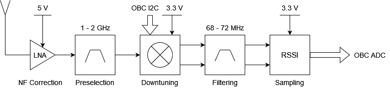
Now the above diagram will be explained from left to right:
Initially, the RF signal is received by the antenna and sent through a L-Band filter and amplified. The signal then enters the mixer to down-convert its frequency to the RSSI (Received Signal Strength Indicator) chip band. After that, the signal passes through a narrow band filter to prepare it for RSSI measurement. The RSSI captures the signal and converts the detected power into voltage. Finally, the processed signal is handled by the Payload software, which is the central matter of interest of this page.
K-band Payload
K-band Payload will monitor the 24 GHz to 25 GHz band, and will consist of two 4x4cm2 PCB.
Below here is the block design of the payload:
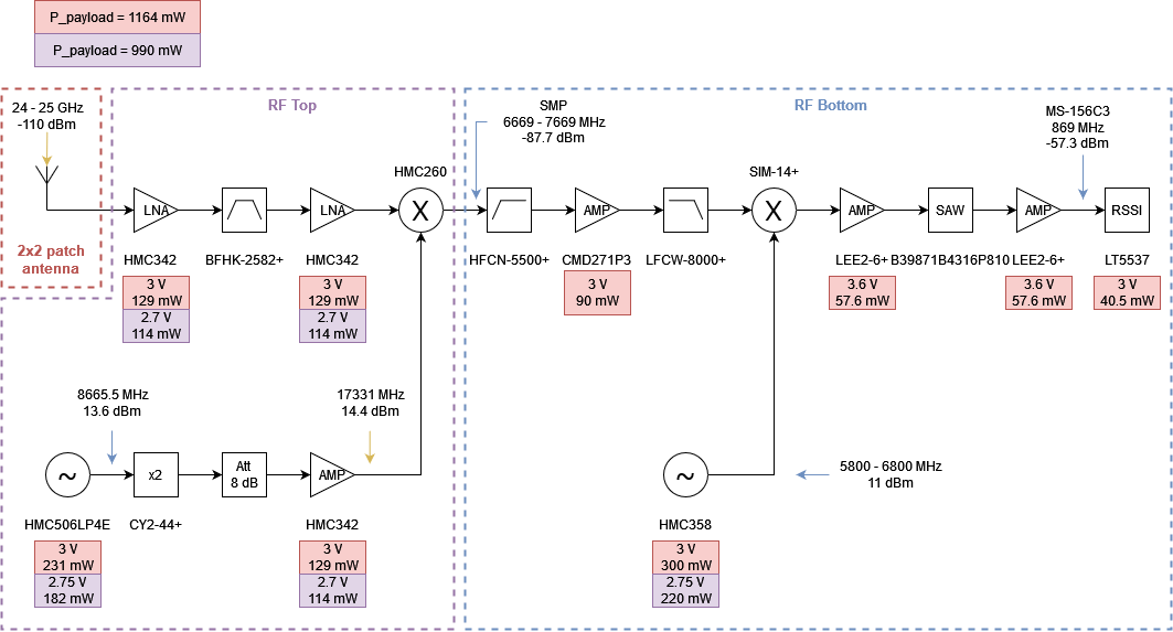
As it can be seen above, the system is divided in two main parts, the RF (Radio Frequency) part and the IF (Intermediate Frequency) part.
The RF part is the one in charge of capturing the RF signal at 24-25 GHz, filtering and amplifying it and downconverting it to an Intermediate Frequency. Then, the IF part is in charge of, again amplifying, filtering and lowering the signal for the RSSI input, to finally measure it as best as possible.
It is also notable to say that the first mixer is fixed in order to get an specific IF. And the last mixer is the one in charge of sweeping its frequency to analyze the signal divided in frequency bins.
In conclusion, the advantage of this implementation is that, although both payloads operate internally in different ways, only the antenna and oscillator operation differ. Furthermore, the final RSSI in both payloads is similar, so the OBC reads them in the same manner.
Software design: RFI dedicated Thread
To control the payloads and collect, process and store the data generated by them, a dedicated thread is used. In this section the thread functionment and data processing done by the dedicated thread.
RFI Thread
Introduction
Like many other subsystems, the Payload is a self-contained sub-system and so it has its own FreeRTOS Thread. This thread is concieved to be able to control each of the two RFI monitoring payloads.
As an overview, the thread is structured as secuential general operations. And each of them is a key step in the process of making the payload work.
Block Diagram
To begin, the general behavior of the code is defined, since it is basic to have it structured from the most generic functions to the most specific ones. This general structure is basic since it is the one that will be in direct ”contact” with the OBC code, and its structure and functioning requirements.

This figure, as stated above, defines how the payload code is structured and its sequential steps. Note that the discontinuous arrow indicates that once the loop has finished, the payload thread enters a sleep mode, waiting for the OBC to awaken him again to restart the loop. So, the first to take a deeper look into is going to be the Check start conditions block:

As it can be seen above, the first thing to do in order to get the payload running properly is to check if the conditions required by the Ground Station user are met, this includes three things:
- The satellite is pointing at the desired region of the Earth steadily.
- The order to make an RFI measurement has been truly received.
- It is the scheduled moment to take the photo.
If none of these requirements are met, the thread awaits until it is signaled by the OBC and then rechecking everything again. Once the check has been succeed, it is time to Start the electronics and the timer:

Obviously, the first step is to power on the payload and consequently all its elements. Then the ADC and DAC are initialized and started. The same happens to the timer. Once they have been started it is time to make sure that they work as expected:

Now the ADC and DAC are checked and calibrated, the timer is only checked. This is done to assure that when using them in the measurements they don’t give false reading due to a malfunction. Having everything powered on, initialized and checked, the measure loop can begin:

This loop is run as many times as needed in order to scan all the frequency bins forming the L or Ka bands. This scans are slow, so not to block the whole satellite system, every time a frequency bin is scanned the thread checks for notifications coming from the rest of the PQ to pause itself if necessary. Then, once the satellite does not need to have the RFI thread stop anymore, the RFI thread continues from where it was.
In order to bring the explanation to a lower level, the list below explains each block step by step:
- Prepare variables: Every variable that is going to be used during the measure loop execution needs to be initialized to ensure a solid structure in the RAM (Random Access Memory).
- Configure DAC: The DAC (Digital to Analog Converter) is configured to make the oscillator output a certain frequency (depending on the frequency bin that wants to be analyzed) by inputting the accordingly calculated voltage.
- Wait X ticks: a yet to be calculated amount of clock ticks is waited to ensure that the frequency from the CO (Controlled Oscillator) is stable.
- The amount of ticks needed depends on the clock speed, and DAC configuration and stabilisation time, which can be found in the microcontroller datasheet. The amount of ticks awaited must exceed an equivalent time of 7.5us.
- This calculation is done taking into account the clock speed and therefore the tick period. This results in the next formula: X = 7.5/fclk[MHz]
- Read ADC N times: The ADC reads the voltage from the RSSI output and converts it to a digital value. This is done N times for the posterior time domain analysis of the samples. The value of N is calculated by dividing the BW (Bandwidth) of the band with the RSSI BW, resulting in the next formula: N = BW/BWRSSI .
- For the L band: Since the RSSI BW is 4 MHZ, the resulting N = 250 .
- For the Ka band: Since the RSSI BW is 16 MHZ, the resulting N = 63 .
- Process Data: With the raw ADC (Analog to Digital Converter) values, calculate different statistical parameters to represent that frequency bin. Those will be stored, whereas the raw values will not.
- Store Data: Store the data mentioned before in a array that will store the statistical data from each frequency bin.
Now that the measurements have been done, it is time to power off this subsystem:

So, first both ADC and DAC are stopped, then the payload is powered off and then the timer is stopped.
To finish the thread execution, the end of the payload work is signaled to the OBC and then the thread enters sleep mode.
Detection algorithms
Temporal algorithm
The aim of this sub-algorithm is to detect pulses through Envelope Detection, a straightforward technique used for RFI monitoring. It involves sampling the input signal and comparing its power with a predetermined threshold. The detector continuously observes the power of the received signal in each temporal sample and establishes a threshold based on the typical noise floor level. When the power level of the samples exceeds this threshold, the detector interprets it as a presence of RFI.
Although the Envelope Detection algorithm has been chosen, other time domain detection algorithms exist such as the FFT (Fast Fourier Transform) based ones. FFT is the most important calculation when talking about time sampled signal processing because it allows to not only analyse the signal in the temporal domain but also in the frequency one. And by combining these two ones, advanced algorithms can be elaborated.
In addition to that, despite the very limited processing capabilities of the microcontroller used in the satellite, some advances are being done. Some preliminar tests have already proven the possibility to compute FFTs in that microcontroller. In the following weeks the integration of those algorithms with the rest of the code will be tried and tested.
Now the mathematical algorithm will be explained. First, the temporal samples vector, expressed as: 𝑥[𝑛];being N the number of samples taken Is iterated in order to calculate its mean:
Finally, if the 𝑥 is higher or lower than an arbitrary threshold the decision of whether there is in fact a signal or not is taken. This threshold is the most important part of the algorithm and its value highly affects the accuracy of the decision.
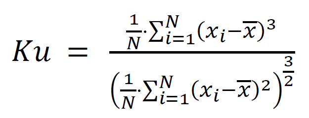
Statistical Algorithm
The purpose of this sub-algorithm is to estimate if there are signals based on their third and fourth statistical moments. These moments are extracted from the temporal samples taken in each frequency bin.
However, there are many other statistical parameters that can be taken into account, such as the standard deviation, the covariance or the correlation. Unlike the reason above, these parameters will not be used because they are not considered necessary with the given skewness and kurtosis reliability.
Now the kurtosis formula will be explained:

Where: 𝑥𝑖 is the i-th sample.
In the numerator of the fraction there is the calculation of the fourth statistical moment, while in the denominator there is the standard deviation elevated to the fourth power. Now the skewness formula will be explained:
Where: 𝑥𝑖 is the i-th sample.
In the numerator of the fraction there is the calculation of the third statistical moment, while in the denominator there is the standard deviation elevated to the third power.
Again, as explained in the time domain algorithm, the decision of the statistical algorithm is based on the comparison between the statistical parameters and predefined thresholds that, if exceeded or not, a decision is then made.
Frequency Algorithm
The aim of this sub-algorithm is to detect signals in the frequency domain and eventually mitigate them by frequency blanking. This technique operates in a similar manner to Envelope Detection, but in the frequency domain. If a significant increase in power is observed at a particular frequency bin compared to its neighbouring bins, it may indicate the presence of interference. These power peaks are more easily detected when they have high power in a narrow bandwidth.
This analysis is done by comparing the received power from adjacent frequencies and applying a threshold to distinguish these values. So, if the algorithm detects a signal that is above that threshold, it decides that it is in fact an Interference.
Subsystem Verification Test - SSV
Test Description and Objectives
The objective of this test is to validate the correct operations of the P/L2 L-band RFI monitoring payload board layout, the quality of the data acquisition process, as well as the deployment and operation metrics of the Helical antenna. This test is meant to be performed both upon each new board assembly, as many of the errors discovered with this test are manufacturing-related and thus repeatable, as well as after any environmental test on the same board.
Requirements Verification
| ID | Description | Status |
|---|---|---|
| M-0700 | The L-band receiver antenna will be omnidirectional, operate in the 1-2 GHz band and feature a reflection coefficient greater than 6 dBs. | Ok |
| M-0710 | The L-band receiver antenna will be contained inside the satellite's allowed space envelope during launch and capable and controlled deployment once in orbit | TBC |
| M-0720 | The L-band receiver front end will be compatible with the rest of the satellite in terms of power requirements and data exchange and storage capabilities. | TBC |
| M-0730 | The L-band receiver front end will attain a 5 MHz or better frequency resolution. | TBC |
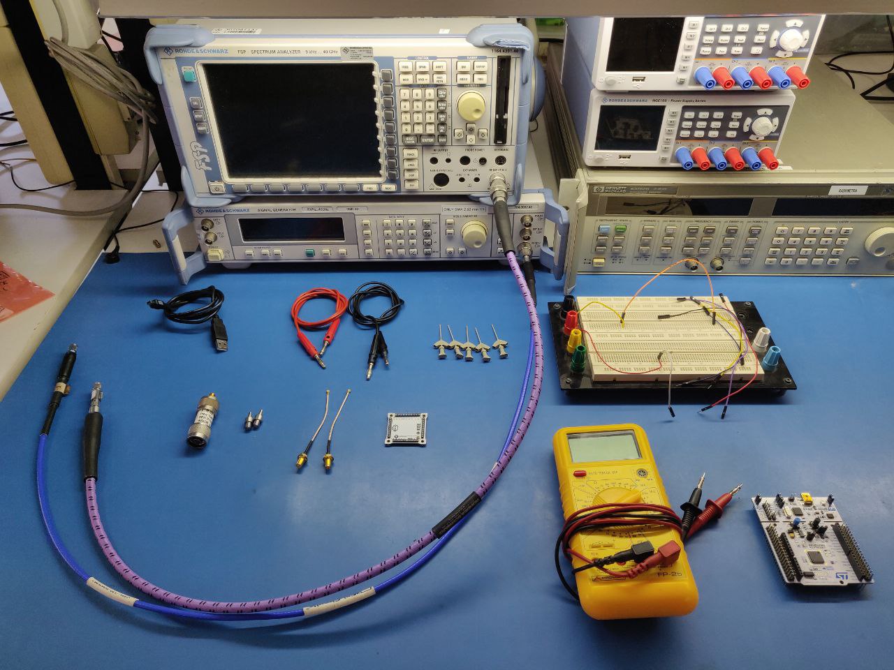
Test Set-Up
For performing this test, the following items are required:
- 1 completely soldered P/L2 board.
- 1 breadboard
- 2 male to male jumper cables
- 5 male to female jumper cables
- 5 handsfree oscillocope probe
- 2 banana-banana power cables
- 1 multimeter with sharp termination cables
- 1 power supply
- 1 Signal generator (10 MHz - 3 GHz)
- 1 Spectrum Analyser (up to 3 GHz)
- 1 SMA DC block
- 2 SMA to SMA 50 ohm coaxial cables
- 2 SMA to U.FL header transition
- 2 SMA to MS156 probe transition
- 1 OBC board with at least the STM and pull up resistors soldered OR a Nucleo board + PC with SMT32Cube IDE + USB to mini USB cable
In what follows the pinout of the P/L2 board will be explained. It is worth mentioning that the vertical pinout is shared by all boards of the PQ, so in case an OBC board is used, the connection can easily be done by simply mounting the 2 PCBs together using the vertical connectors. The pins used for this test are the folowing:
| Connector index | Pin position | Name | Description |
|---|---|---|---|
| J1 | 1 | SDA1 | I2C data bus 1 (reserved for payloads) |
| J1 | 2 | SCL1 | I2C clock bus 1 (reserved for payloads) |
| J1 | 9 | GND | Global Ground pin |
| J1 | 10 | VCC | Global supply line (3.3V but not for P/L2) |
| J2 | 7 | GND | Global Ground pin |
| J2 | 10 | GND | Global Ground pin |
| J3 | 2 | PH6 | +Y photodiode pin (post amplification) |
| J3 | 6 | P/L_Power | PoL - controlled supply line (3.1 V) |
| J4 | 8 | DAC | OBC STM32 Digital-to-Analog output pin |
| J4 | 9 | ADC | OBC STM32 Analog-to-Digital input pin |
They can be located as follows in the vertical top (left) & bottom (right) views shown below:

Next up, the steps for the connections will be presented. They need to be replicated whenever a new test sub-section is performed, unless stated otherwise.
- Mount the OBC&COMMS and P/L2 board together using the vertical connectors. Make sure that both of them match the rotation configuration.
A light mounting is recommended as not to fully latch the pins which will make subsequent separation of the boards difficult. If however, for any reason, vertical mounting is not feasible OR if a Nucleo Board is chosen to be used instead of the OBC&COMMS board, then the connection of all pins shown above except VCC and GND should be done with male-female jumper cables, using oscilloscope probe endings to better latch to the P/L2 male vertical pins.
-
Power on the power supply with the OUTPUT DISABLED and set it to 3.3 V with a current limit of 500 mA, connecting it using the banana connectors to the breadboard.
-
Using 2 jumper cables of preferably distinctive colours (red for supply and black for GND), connect the breadboard GND to any of the GND pins shown in the pinout above, and the breadboard supply to the VCC pin. The reader should also use this opportunity to understand how the powering of this payload is done.
As the payloads are duty-cycled consumers whose activation needs to be strictly controlled, their supply is done through a PoL (point of load) switch located on the OBC board that, upon activation with a GPIO (General purpose Input/Output) pin of the STM32, enables the 3.3V permanent voltage line of the PocketQube to supply the P/L board through the P/L_Power pin. As a result, during this test, as this SSV aims at testing the payload under the same conditions as those encountered in orbit, the powering has been chosen to be done the nominal way, from the 3.3V VCC all the way through the OBC-controlled Pol, through the P/L_Power pin and into the actual payload board. It warrants mentioning however that, if someone would like to test exclusively the P/L2 board OR if the Nucleo Board approach has been chosen, direct powering through the P/L_Power pin is possible (in which case the power supply is directly connected to the latter pin, with the VCC pin not seeing use).
-
Power on the signal generator with the OUTPUT DISABLED and carefuly connect the 50 ohm SMA-SMA coaxial cable to its output. Attach the SMA to U.FL adaptation to the other end.
-
Power on the spectrum analyser and very carefully attach a DC block directly to its input. Then connect to the free end of the DC block a SMA-SMA 50 ohm coaxial cable. Do not attach any of the remaining U.FL or MS-156 adaptations yet, as the type needed depends on the sampling point.
-
Enable the power supply output and verify that the SMT32 is correctly powering on and that the latest version of the P/L2 task software is flashed.
For details on STM32 operation, please refer to the OBC page within ³Cat-NXT Design chapter. Before continuing from this point, the reader should be able to operate the STM at least in what regards the I2C bus, ADC input and DAC output, as well as flash the newest version of the software.
After a test session is completed, regardless of the length of the hiatus, one should proceed to disable the signal generator and power supply (in this order), disconnect all the cables (very gently in the case of the U.FL and MS156 terminations), power off all equipment and safely store all cables in their designated bags, terminations apart, and place the item under test in an antistatic bag equipped with a silica bag.
Pass/Fail Criteria
This test will be considered passed if all of the following actions are performed succesfully:
- The code executes correctly upon flashing.
- A 2 GHz band noise-level sweep centered at 1.5 GHz is correctly filtered, amplified, downconverted to 70 Mhz within a 4 MHz bandwidth.
- The resulted signal is translated by the RSSI into the appropiate voltage according to the manufacturer's specifications.
- The data aquisition process is correctly performed with the data being accessible from the STM32's flash memory banks.
Test Plan (By Subblocks)
Before moving towards the testing of the whole subsystem, in order to single out possible errors, the payload's isolated segments will be tested a part, starting for simplicity with those which do not require a STM32 (be it a Nucleo Board or the OBC&COMMS board) to be verified.
5V booster
The 5V booster, in the form of LT3048, is needed to augument the line voltage of 3.3 V of the PocketQube to 5 V in order to correctly supply the LEE2-6+ LNA. The testing procedure for it is listed below:
-
Ensuring that the correct connections have been done as per the Test Set-Up section above, enable the output of the power supply.
-
If the OBC&COMMS board approach has been chosen, also activate the P/L2 PoL via the IDE used to debug the task software. If feeding the board directly through the P/L_Power pin, then skip this step.
-
Check the current drain of the power supply. It should be around the value of XXX mA.
-
Using the multimeter set in voltage mode, measure the voltage between the P/L_Power pin and GND. It needs to be between 3.3 V and 3.1 V.
-
With a sharp multimeter termination, as looking at the BOT side of the board, gently sample the left terminal of the R1 resistor and GND. The value should be about 5 V. If it is the case, it can be concluded that the booster works properly.
RF chain Low Noise Amplifier (LNA)
In the form of the LEE2-6+, fully explained in the appropiate P/L page, under the ³Cat-NXT Design chapter, the LNA is supposed to provide a gain between 20.6 dB (at 1 GHz) and 18.9 dB (at 2 GHz) over the L-band. To test this feature, a signal will be introduced at the receiver's input, and sampled from the first RF chain probe. The procedure is as follows:
-
Not having modified the configuration done in the 5V booster subsection, the board should be operational. This can be checked by having a current consumption of cca xxx mA seen on the power supply display and with a voltage between 3.1 V and 3.3 V measured between the P/L_Power and GND pins. If otherwise, repeat the previous sub-section steps.
-
Connect the signal generator output through the SMA-U.FL termination to the J5 coaxial header located on TOP side of the board, lower right corner.
-
Attach a SMA-MS156 probe termination to the free end of the coaxial cable of the spectrum analyser and connect it to the J6 MS156 probe header found on the BOT side of the board, on the left hand side.
The MS156 probes act like an electrically closed circuit when in nominal state, but disconnect the subsequent circuit when probed. This means that probing cuts elements further on the transmission line from the input, in this case anything past the J6 probe: bandpass filter, tuner, IF chain, etc...
-
Set up the spectrum analyser to a center frequency of 1.5 GHz, a span of 2 GHz (having a total observable window from 500 MHz to 2500 MHz) and using the maxim Autopick setting for ease of interpretation.
-
With the board and LNA powered as detailed above, select a tone of -50 dBm in ampltude and 1 GHz of frequency on the signal generator and then enable its output.
-
Observe the reading on the spectrum analyser. The same tone inputted should be visible, but with an amplitude gain of cca 20 dB. Note down any frequency shift if the case and take screen captures as needed.
-
Repeat the last two steps, this time at a number of different frequencies from 1 GHz to 2 GHz. It is recommended to do so at 200 MHz apart.
-
If the gain observed along said measurements coincides with the values provided by the manufacturer within a 5% tolerance, this test is considered passed. Note that the values of gain according to the datasheet are: 20.6 dB (1 GHz), 20.3 dB (1.2 GHz), 19.9 dB (1.4 GHz), 19.6 dB (1.6 GHz), 19.3 db (1.8 GHz) and 18.9 dB (2 GHz).
Bandpass filter
The BFCG162W bandpass filter's function is to preselect the signal within a range indicated by the manufacturer to be between 950 MHz and 2200 MHz, with an insertion loss of lower than 3 dB in-band and higher than 20 dB out-of-band. These characteristics can be tested as follows:
-
With the configuration from the Set-Up section in place as well as the OBC PoL turned on, connect the SMA-MS156 ended cable of the spectrum analyser to the J7 MS156 probe header found on the BOT side of the board. Make sure that the previous connection to J6 done in the previous sub-section using the MS156 is removed, in order to return the probe header to its electrically closed morphology.
-
Make sure the output of the signal generator is still connected through the J5 U.FL coaxial header on the TOP side of the board
-
Set up the spectrum analyser to a center frequency of 1.5 GHz, a span of 2 GHz (having a total observable window from 500 MHz to 2500 MHz) and using the maxim Autopick setting for ease of interpretation.
-
Configure the signal generator to output a 500 MHz - 2500 MHz frequency sweep of -50 dBm amplitude and enable its output.
-
Observe the resulting signal on the spectrum analyser. The frequency components outside of the 950 MHz - 2200 MHz range should show an attenuation of at least 20 dB, with the in-band components not decreasing more than 3 dB. If the previous statements are empirically proven true, then it can be concluded that the bandpass filter is operational.
Downconversion tuner
The downconversion of this receiver is done using the I2C controlled MAX2121 VSSAT tuner, from the 1-2 GHz RF chain to the 70 MHz IF chain, by applying a frequency sweep. Worth mentioning is that the task software verification is only subject to verification in the functional sense in this test, and it is explained in detail in ... Additionally, it is the last item of this receiver's front end to allow separate verification of sorts, as the subsequent IF chain is a differential line with no probing point, followed by the adaptation network of the RSSI and the RSSI itself. Therefore, the steps to follow are:
-
Make sure that the configuration from the Set-Up section is in place.
-
Verify that the OBC PoL is turned on and the DAC pin holds a voltage of 2.7 V.
-
Leave the signal generator unconnected and its output disabled. Remove any MS156 probe termination that might have remained attached from previous tests.
-
Attach a SMA-U.FL probe termination to the free end of the coaxial cable of the spectrum analyser and connect it to the J8 U.FL coaxial header found on the BOT side of the board, in the central region of the PCB.
-
Set up the spectrum analyser to a center frequency of 1.5 GHz, a span of 2 GHz (having a total observable window from 500 MHz to 2500 MHz) and using the maxim Autopick setting for ease of interpretation.
-
By using the IDE, set the downconversion tuner's local oscillator frequency between 930 MHz and 1930 MHz with steps of 50 MHz.
-
On the spectrum analyser's display, deltas of frequencies corresponding to those set in the software should appear. Note down any frequency shift. If the frequencies match with a 5 MHz tolerance, the isolated testing of the downconversion tuner is concluded with success.
Photodiode Opamp
-
Make sure that the configuration from the Set-Up section is in place as well as the OBC PoL is turned on.
-
Orient the board towards a sufficiently luminous source and sample the voltage at the terminals of the photodiode. Write the value down. It should be small (micro or nano volts) but non null and varying with the degree of luminosity.
-
Using a sharp termination multimeter and without moving the board any longer (as not to change luminous conditions), sample the voltage this time between the PH6 and GND pins. Write down the value. Ihe value should be cca 20 times bigger. If the case, then it can be concluded that the photodiode and its opamp block are operating as expected.
Test Plan (Full subsystem)
From this point the document is a stub.
Having tested and isolated possible errors as much as possible in a bit-by-bit manner in the previous section, a full subsystem test will now be performed.
-
Make sure that the configuration from the Set-Up section is in place as well as the OBC PoL is turned on.
-
Connect the signal generator output through the SMA-U.FL termination to the J5 coaxial header located on TOP side of the board, lower right corner. It is recommended that at least the first full SSV is done by way of signal generator input, with later tests possibly replacing this input with the real one by way of the antenna in order to firstly test the front end separate from any possible errors.
-
Configure the signal generator to output a 500 MHz - 2500 MHz frequency sweep of -100 dBm amplitude with random spikes at -80 dBm and enable its output.
-
Using the IDE, initiate the P/L task within the STM32, using the full PQ firmware scheduler.
-
Using the Umbilical connection, download the flash memory experiment files.
Test Results
Description of the Test results (photos, tables, etc) with interpretation.
5V booster test:
RF chain LNA test:
Bandpass filter:
Downconversion tuner:
Photodiode Opamp:
Full subsystem test:
Anomalies
List of deviations to the Test Specification and Procedure and non-conformances witnessed during the test campaign, including a brief description, the close-out status and reference to the relevant reports.
Conclusions
Verified requirements (and within which part of the test), close-out judgement (compliance status) and rationale, statement of open issues and possible remediating actions