The objective of this test is to validate the correct operations of the P/L2 K-band RFI monitoring payload board layout, the quality of the data acquisition process, as well as the deployment and operation metrics of the Helical antenna. This test is meant to be performed both upon each new board assembly, as many of the errors discovered with this test are manufacturing-related and thus repeatable, as well as after any environmental test on the same board.
| ID | Description | Status |
|---|---|---|
| M-0700 | The L-band receiver antenna will be omnidirectional, operate in the 1-2 GHz band and feature a reflection coefficient greater than 6 dBs. | Ok |
| M-0710 | The L-band receiver antenna will be contained inside the satellite's allowed space envelope during launch and capable and controlled deployment once in orbit | TBC |
| M-0720 | The L-band receiver front end will be compatible with the rest of the satellite in terms of power requirements and data exchange and storage capabilities. | TBC |
| M-0730 | The L-band receiver front end will attain a 5 MHz or better frequency resolution. | TBC |
This specifications should be further detailed? To clarify the SSV results
For performing this test, the following items are required:
Below is the connections schematic:
Configure to desired parameters
Set up nucleo board and PC
This test will be considered passed if all of the following actions are performed succesfully:
The signals inputed and their supposed detection is yet to be completely characterized.
Before moving towards the testing of the whole subsystem, in order to single out possible errors, the payload's isolated segments will be tested a part, starting for simplicity with those which do not require a STM32 (be it a Nucleo Board or the OBC&COMMS board) to be verified.
In the form of the HMC342, fully explained in the appropiate P/L page, under the ³Cat-NXT Design chapter, the LNA is supposed to provide a gain of arround 19dB (at 24-25 GHz) over the Ka-band. To test this feature, a signal will be introduced at the receiver's input, and sampled from the first RF chain probe. The procedure is as follows:
First of all, the board should be operational. This can be checked by having a current consumption of cca 230 mA seen on the power supply display and with a voltage between 3.1 V and 3.3 V measured between the P/L_Power and GND pins. If otherwise, repeat the previous sub-section steps.
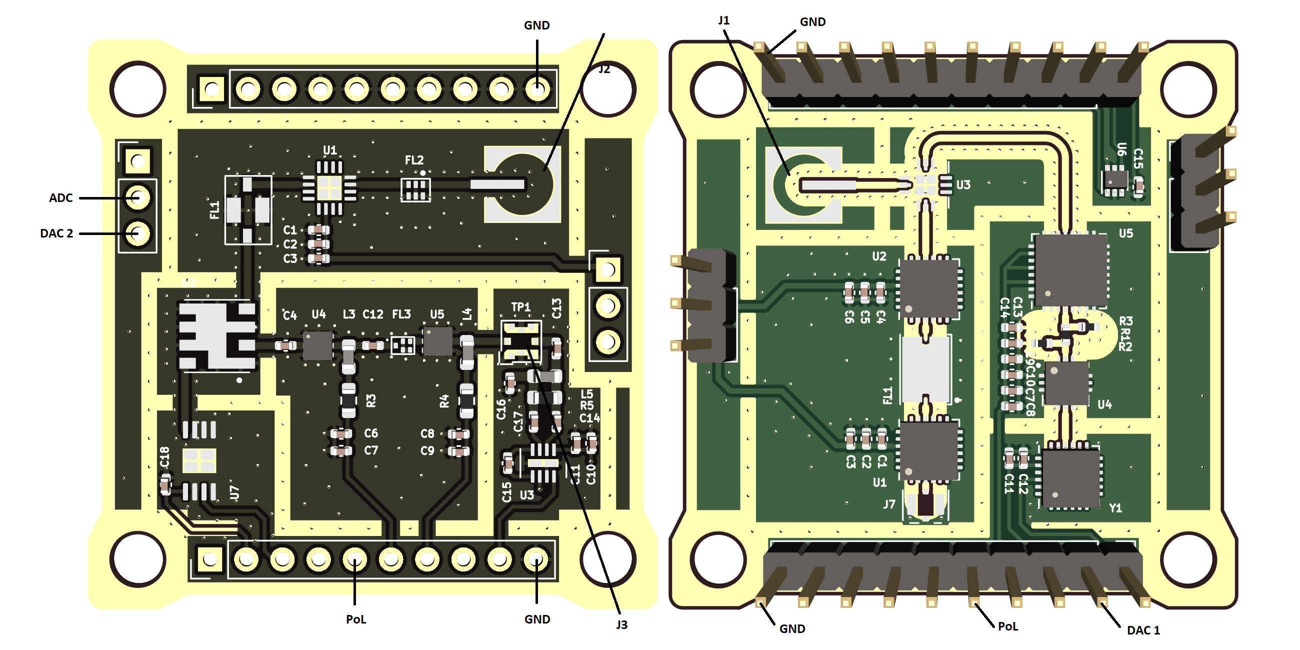
Connect the signal generator output through the SMA-U.FL termination to the J1 coaxial header input connector.
Attach pin probe termination to the free end of the coaxial cable of the spectrum analyser and connect it to the output pin of the LNA.
Set up the spectrum analyser to a center frequency of 24.5 GHz, a span of 2 GHz (having a total observable window from 23.5 GHz to 25.5 GHz) and using the maxim Autopick setting for ease of interpretation.
With the board and LNA powered as detailed above, select a tone of -80 dBm in ampltude and 24.5 GHz of frequency on the signal generator and then enable its output.
Observe the reading on the spectrum analyser. The same tone inputted should be visible, but with an amplitude gain of cca 19 dB. Note down any frequency shift if the case and take screen captures as needed.
Repeat the last two steps, this time at a number of different frequencies from 24 GHz to 25 GHz. It is recommended to do so at 100 MHz apart.
If the gain observed along said measurements coincides with the values provided by the manufacturer within a 5% tolerance, this test is considered passed.
Once the LNA is proven to work fine, the filters mut be checked. For these operations the same procedure is followed.
Connect a 50 Ohm matching load to the SMA-U.FL termination to the J1 coaxial header input connector, the RF Input.
Attach a pin probe termination to the free end of the coaxial cable of the spectrum analyser and connect it to the output pin of the filter.
This step is detailed for each filter.
If the BW observed along said measurements coincides with the values provided by the manufacturer within a 5% tolerance, this test is considered passed.
Set up the spectrum analyser to a center frequency of 24.5 GHz, a span of 2 GHz (having a total observable window from 23.5 GHz to 25.5 GHz).
Set up the spectrum analyser to a center frequency of 7169 MHz, a span of 2 GHz.
The B39871B4316P810 bandpass filter's function is to select the signal within a range indicated by the manufacturer to be between 862 MHz and 876MHz, with an insertion loss of lower than 1.6 dB in-band. These characteristics can be tested as follows:
Set up the spectrum analyser to a center frequency of 869 MHz, a span of 50 GHz.
The downconversion of this receiver is done using the voltage controlled HMC260 tuner, from the 24-25 GHz RF chain to the 7 GHz IF chain, by applying a frequency sweep. The steps to follow are:
Make sure that the configuration from the Set-Up section is in place.
Verify that the OBC PoL is turned on and the DAC pin holds a voltage constant controllable voltage.
Connect the signal generator output through the SMA-U.FL termination to the J1 coaxial header input connector.
Attach a SMA-U.FL probe termination to the free end of the coaxial cable of the spectrum analyser and connect it to the J2 U.FL coaxial header, the IF input terminal.
Set up the spectrum analyser to a center frequency of 24.5 GHz, a span of 2 GHz (having a total observable window from 23.5 GHz to 25.5 GHz) and using the maxim Autopick setting for ease of interpretation.
With the board powered as detailed above, select a tone of -80 dBm in ampltude and 24.5 GHz of frequency on the signal generator and then enable its output.
Observe the reading on the spectrum analyser. The same tone inputted should be visible, but with an amplitude loss of 9 to 12 dB. More importantly, the frequency shift must be the one according to the inputed voltage.
Note that the relation between voltage and frequency is not linear and need to be characterized as stated in the VCO calibration procedure
Repeat the last two steps, this time at a number of different frequencies from 24 GHz to 25 GHz. It is recommended to do so at 100 MHz apart.
If the attenuation and frequency shift observed along said measurements coincides with the values provided by the manufacturer within a 5% tolerance, this test is considered passed.
The downconversion of this receiver is done using the voltage controlled SIM-14+ tuner, from the 6669-7669 MHz IF chain to the 869 MHz LF chain, by applying a frequency sweep. The steps to follow are:
Make sure that the configuration from the Set-Up section is in place.
Verify that the OBC PoL is turned on and the DAC pin holds a voltage constant controllable voltage.
Connect the signal generator output through the SMA-U.FL termination to the J1 coaxial header input connector.
Attach a SMA-U.FL probe termination to the free end of the coaxial cable of the spectrum analyser and connect it to the J3 U.FL coaxial header, the IF input terminal.
Set up the spectrum analyser to a center frequency of 7169 MHz, a span of 2 GHz, and using the maxim Autopick setting for ease of interpretation.
With the board powered as detailed above, select a tone of -80 dBm in ampltude and 7169 MHz of frequency on the signal generator and then enable its output.
Observe the reading on the spectrum analyser. The same tone inputted should be visible, but with an amplitude loss of 6.7 to 9.5 dB. More importantly, the frequency shift must be the one according to the inputed voltage.
Note that the relation between voltage and frequency is not linear and need to be characterized as stated in the VCO calibration procedure
Repeat the last two steps, this time at a number of different frequencies from 24 GHz to 25 GHz. It is recommended to do so at 100 MHz apart.
If the attenuation and frequency shift observed along said measurements coincides with the values provided by the manufacturer within a 5% tolerance, this test is considered passed.
From this point the document is a stub.
Having tested and isolated possible errors as much as possible in a bit-by-bit manner in the previous section, a full subsystem test will now be performed.
Make sure that the configuration from the Set-Up section is in place as well as the OBC PoL is turned on.
Connect the signal generator output through the SMA-U.FL termination to the J1 coaxial header. It is recommended that at least the first full SSV is done by way of signal generator input, with later tests possibly replacing this input with the real one by way of the antenna in order to firstly test the front end separate from any possible errors.
Configure the signal generator to output a 24 GHz - 25 GHz frequency sweep of -100 dBm amplitude with random spikes at -80 dBm and enable its output.
Using the IDE, initiate the P/L task within the STM32, using the full PQ firmware scheduler.
Using the Umbilical connection, download the flash memory experiment files