ᴾᵒCat: RFI K-Band Payload
In this book information about ᴾᵒCat-3 P/L , a RFI Monitoring payload in the K-Band, is found including a subsystem description hardware and software designs as well subsystem verification.
- RFI-5G Mission Analysis and Requirements
- RFI-5G Design
- RFI-5G Payload block diagrams
- RFI-5G Payload design
- Antenna Design
- Data Acquisition
- RFI-Dedicated Thread
- Test
- RFI-5G FE-Bottom SSV
- RFI-5G FE-Top SSV
- K-Band VCO Calibration Procedure
- Front-end Gain calibration Procedure
- K-band Noise floor characterization Procedure
- K-band CW characterization Procedure
- P/L3 Envelope Detection characterization Procedure
- P/L3 Statistical pulsed signal characterization Procedure
- Tests as Run
RFI-5G Mission Analysis and Requirements
Project description
This project is performed as part of the IEEE Geoscience and Remote Sensing/Frequency Allocations in Remote Sensing (GRSS/FARS) Technical Committee project to monitor the spectrum with the 24 GHz water vapor band and the low part of the 5G 26 GHz band.
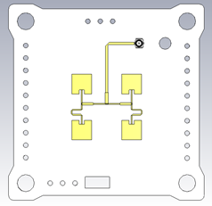
The system has to be able to perform a power spectrum analysis dividing the 24-25 GHz band in smaller parts and output a voltage level related with the power of said part measured at the input. The system has to be small enough to fit in a PocketQube, a 5 cm side cubic picosatellite.
The payload is to be flown in two ways with the same configuration: as a satellite and drone attached to a drone.

Image not to scale
Requirements
| RFI5G_010 |
The payload shall measure input powers of -110 dBm in 10 MHz bands. |
| RFI5G_020 | The payload frequency resolution has to be smaller or equal than 10 MHz. |
| RFI5G_030 |
The payload output has to be an analogue voltage between 0 and 3.3 V. |
| RFI5G_040 | The payload's maximum peak power consumption has to be smaller than 1.5 W. |
| RFI5G_050 | The payload's average power consumption has to be smaller than 0.5 W. |
| RFI5G_060 | The payload has to interface with the "IEEE Open PocketQube". |
| RFI5G_070 | The full PocketQube weight with the payload has to be smaller than 250 g. |
| RFI5G_080 | The payload's non-operational temperature has to range from -40 to 80 ºC. |
| RFI5G_090 | The payload's operational temparature has to range from 0 to 45 ºC. |
Operation Conditions:

Pyload Execution:

RFI-5G Design
RFI-5G payload designs. Includes electrical, mechanical and software.
RFI-5G Payload block diagrams
FE Block Diagram

Power Supply Block Diagram

Signal Conditioning Block Diagram

4. General block diagram

RFI-5G Payload design
IGARSS_2023_Kband_RFI_Paper.pdf
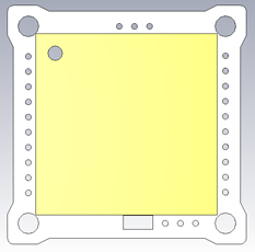
Payload Structure
The payload is structured as a vertical stack of PCBs, like the rest of the satellite. This is done in order to be self-contained and to comply with the IEEE Open PocketQube Kit standard.
This stack is designed so that the interferences from upper layers cannot penetrate down to the lower side and so the rest of the PocketQube. This isolation is mainly achieved thanks to the Structural piece, the aluminum shield, which connects the grounding from the PCBs in contact with it on both sides, so that it creates a grounded case, creating a Faraday Cage that is able to enclose the interferences radiated from within while also isolating those from the radiation coming from the exterior.
Another relevant structural component is the FR-4 Structural PCB. The only purpose of this PCB is to support the K-Band Antenna, which is very delicate and thin.
In both cases the Antenna and Top PCB with the FR-4 Structural and the Bottom PCB with the Interface they are attached with epoxy glue and soldered pins when possible. This ensures a good rigidity and a proper performance when faced the important vibrations produced during launch.

Payload Pinout

Schematics
Interface PCB
The Interface PCB is in charge of doing 3 main things:
- Regulating the voltage from the satellite to provided the needed ones to the different components of the payload.
- Creating a reliable voltage source for the voltage dependant components of the payload such as VCOs.
- Regulating the voltage output from the RSSI block of the payload, ensuring reliable measures.
This is why the interface schematic if divided into three parts.

LDOs
This stage is in charge of regulating the 3.3V voltage line from the PQ to the various required voltage needed in the payload.
| Voltage |
Target component |
| 2.5V |
IF1Amp |
| 2.7V |
LNA2 |
| 2.75V |
|
| 3V |
To be finished
The schematic below shows the design of the voltage regulation circuit for the payload. The purpose of this circuit is to provide stable, regulated power at various voltage levels required by different components within the payload, which is essential for reliable and accurate signal processing and data collection.
Now an in-depth look at the decisions made in the design will be done:
1. Voltage Regulators (U4 and U5 - MIC2215 Series)
- The MIC2215-AAAYML-TR voltage regulators (U4 and U5) were chosen for their low dropout characteristics and stable output. Low dropout regulators (LDOs) are essential in this design to maintain a consistent voltage output even when the input voltage is only slightly higher than the desired output. This is crucial in space applications or sensitive RF equipment, where power stability impacts the system’s overall performance and noise levels.
- Each LDO is configured to provide a specific voltage level, with U4 supplying one line and U5 supplying another. This setup allows for isolated, stable power lines to reduce cross-interference and ensure that each component receives the necessary voltage.
2. Decoupling Capacitors
- Several capacitors (e.g., C19, C20, C28, etc.) are placed near the voltage regulators and along the power lines to filter out noise and provide a stable DC output. The use of 4.7 µF, 1 µF, and 0.1 µF capacitors at different points serves to filter high-frequency noise and smooth out any power supply variations, a critical step in RF designs where signal integrity can be affected by noise.
- C19 and C32 are examples of capacitors placed close to the MIC2215 regulators, following best practices for power integrity, following the recommended application circuit guidelines provided by the chip manufacturer. These capacitors stabilize the output voltage by providing a reservoir of charge that can quickly respond to changes in load, ensuring the voltage remains stable.
3. Voltage Dividers and Feedback Networks
- Resistor networks, such as R9 and R10 for U4 and R25 and R24 for U5, are used to set the output voltages of the LDOs. These resistors form a voltage divider, which provides feedback to the regulator to maintain the correct output level.
- Careful resistor selection here ensures that each voltage line precisely matches the requirements of the connected payload components, which may be sensitive to even minor fluctuations in voltage. For example, some RF components may have strict voltage limits, and a deviation could cause issues in performance or even damage the part.
4. Separate Power Lines for Isolation
- The circuit includes separate voltage lines, labeled LDO_extra1 and LDO_extra2, with respective voltages indicated as 2V5 and 2V7. These lines likely provide power to different functional blocks within the payload, such as an amplifier (Vcc_IF_Amp) and possibly another component at a similar voltage level but requiring isolation.
- This isolation prevents unwanted interference between different parts of the circuit. In RF designs, where signal fidelity is paramount, isolating power sources for different blocks helps to minimize cross-talk and reduce the risk of interference affecting the sensitive RF signals being processed.

Voltage Boosters
This schematic provides a look at a voltage-boosting circuit. Here, three independent boost converter stages are built around the LT3048IDC-TRMPBF component (U1, U2, and U3). Each of these stages is responsible for generating a specific voltage required by various components in the payload, focusing on boosting an input voltage to a higher, stabilized output for sensitive RF systems.
Here is an expanded explanation of the design decisions and key aspects:
1. Boost Converter ICs (U1, U2, and U3 - LT3048IDC-TRMPBF)
- The LT3048IDC-TRMPBF is a low-noise, high-voltage boost regulator designed to step up an input voltage to a higher output with high efficiency. The choice of this IC is likely due to its high efficiency and ability to handle low-noise applications, which is essential in RF systems where noise can affect signal quality.
- Each boost converter serves a different voltage rail: LEE1_Vcc, LEE2_Vcc, and 13V. This flexibility allows the system to provide stable, isolated voltage lines to multiple components with distinct power requirements.
2. Input Filtering Components (L1, L2, L3, C24, C25, C27)
- Inductors L1, L2, and L3 (5.6 µH) and input capacitors C24, C25, and C27 (100 nF) are placed at the input of each boost converter to filter the incoming voltage. The inductors help smooth out the current, while the capacitors act as decoupling components to suppress high-frequency noise that could affect the boost conversion process.
- This filtering helps to ensure a clean input voltage, which is crucial for stable and efficient operation of the boost converter. In RF systems, this is especially important to avoid coupling of noise into the RF circuitry, which could degrade signal integrity.
3. Output Voltage Feedback and Resistor Networks
- Each boost converter uses a resistor network (e.g., R1, R2 for U1; R3, R4 for U2; and R5, R6 for U3) to set the output voltage. This resistor network forms a voltage divider that feeds back a portion of the output voltage to the FB (feedback) pin, allowing the converter to regulate the output.
- The precise values of these resistors were chosen to produce the desired output voltages (LEE1_Vcc, LEE2_Vcc, and 13V). Accurate resistor selection is critical to achieve stable, predictable output voltages that match the requirements of the connected components, preventing over-voltage or under-voltage conditions that could affect component performance or even damage them.
4. Output Decoupling and Stabilization (C3, C4, C7, C8, C11, C12)
- Each output line includes decoupling capacitors, with 1 µF and 4.7 µF capacitors (such as C3 and C4 for U1) placed in parallel. The 1 µF capacitor provides low-impedance filtering for high-frequency noise, while the 4.7 µF capacitor smooths out lower-frequency variations and transient currents.
- This dual-capacitor approach improves stability and minimizes ripple on the output lines, which is crucial in RF systems where even minor power fluctuations can affect sensitive signal processing circuits.
5. Bypass Capacitors for Noise Reduction
- Small 1 nF capacitors (C2, C6, and C10) are connected to the BYP (bypass) pin of each LT3048 device. These capacitors are used to reduce noise generated by the internal circuitry of the boost converter. The values are chosen according to the manufacturer by following its recommended application circuit.
6. Application-Specific Voltage Rails
- Each voltage line serves a specific purpose, indicated by labels such as LEE1_Vcc, LEE2_Vcc, and 13V. These lines are tailored to the needs of individual components within the RF payload, allowing for optimized power delivery to each functional block.
-
Voltage Line Target Component LEE1_Vcc LEE2_Vcc 13V -
Table to be completed
7. Isolation Between Voltage Rails
- By implementing three separate boost converters, the design provides excellent isolation between the various power lines. This is especially beneficial in RF systems where shared power sources could lead to interference and cross-talk between components.
- Each boost converter effectively acts as its own power supply, with independent regulation and filtering, which minimizes the risk of noise or fluctuations affecting multiple components simultaneously.

Instrumentation Amplifier
This schematic shows an instrumentation amplifier stage used to process the voltage output from the RSSI (Received Signal Strength Indicator) block, which holds the scientific data from the payload. The amplifier conditions this signal so that it can be accurately digitized by the DAC input of the satellite's microcontroller.
Below is an expanded explanation of the main components and design choices within this stage:
1. Instrumentation Amplifier (U6 - AD8224ARZ-R7)
- U6 is an AD8224ARZ-R7 instrumentation amplifier, chosen for its precision and low offset, making it ideal for low-level signal measurements. Instrumentation amplifiers are designed to amplify differential signals while rejecting common-mode noise, a key requirement in this setup, where the output from the RSSI might contain noise from other subsystems or the RF environment.
- The amplifier ensures that the RSSI signal can be accurately amplified and fed to the DAC, preserving data integrity and enhancing measurement accuracy for scientific analysis.
2. Gain Resistors (R15, R16, R17, and R18)
- Resistors R15 (11 Ω), R16 (402 kΩ), and R17 (604 kΩ) set the gain of the instrumentation amplifier. The gain configuration allows fine-tuning of the signal amplification to match the input range of the DAC.
- R18 (73.2 Ω) works alongside the feedback network to provide stability and control over the amplifier’s response, ensuring accurate gain with minimal drift, which is essential for scientific measurements.
3. Input and Output Filtering (C21, C22, C26)
- Capacitors C21 and C22 (both 0.1 µF) are decoupling capacitors that filter out high-frequency noise on the power supply line (13V). Clean power is vital for precision instrumentation amplifiers to avoid fluctuations that could affect amplification accuracy.
- C26 (1 µF) provides additional decoupling on the amplifier's output, further stabilizing the signal before it reaches the DAC. This capacitor helps to smooth out any high-frequency noise that might have coupled through, ensuring a clean, stable signal for digitization.
4. Voltage Divider for Signal Conditioning (R19, R20, R21, R22, R23)
- R19 (64.9 kΩ) and R20 (301 kΩ) form a voltage divider at the amplifier’s output, scaling the amplified signal to the appropriate range for the DAC input.
- Resistors R21 (39.2 kΩ), R22 (255 kΩ), and R23 (49.9 kΩ) form a voltage divider. Also, a voltage divider is used in order to regulate the voltage input to the frist VCO.
5. RSSI Input and Output Connections
- The RSSI label indicates the input connection from the RSSI block, which is a measure of the received signal strength and contains the scientific data output of the payload. The instrumentation amplifier boosts this signal, conditioning it for accurate ADC conversion.
- The amplifier's output is directed toward the DAC_PL2 label, which connects to the DAC input of the satellite’s microcontroller. This connection completes the signal chain from RF reception to digital conversion, allowing the payload’s data to be processed, analyzed, and transmitted.

Bottom PCB
1. IF Input
- The signal enters the circuit through J5, labeled IF1_in, an SMP connector that receives the IF signal from the previous stage on Top PCB.
- IF1_in then passes through a highpass filter, FL2 (HFCN-5500+), which has a cut-off frequency around 5500 MHz. This filter removes any unwanted signals or noise outside the desired IF band, ensuring only relevant frequencies are processed in the following stages.
2. First Amplification and Bandpass Filtering
- After the highpass filter FL2, the signal is then amplified by U1 (CMD217P5), an RF amplifier. This amplifier boosts the IF signal’s strength, improving its signal-to-noise ratio before further processing.
- It is worth mentioning that C1 and C2 (0.33 µF and 100 pF, respectively) are in charge to filter the noise in the voltage line so that the amlifier recieves a clean supply that will not generate further interferences and unnecessary noise.
- After amplification, the signal goes through another lowpass filter, FL1 (LFCW-8400+), with a cut-off frequency around 8400 MHz. This additional filtering stage ensures that the amplified signal remains within the desired frequency range, with any residual out-of-band signals further suppressed.
- The output of this stage is labeled IF1_Out, which carries the filtered and amplified IF signal into the next stage, the mixer.
3. Mixing
This is the most important part in the payload design
- The IF1_Out signal enters the IF2 section, where it is mixed down to a lower frequency. This is achieved by U2 mixer (model SIN-34+), which combines the incoming IF signal with a LO signal from LO2.
- The mixer’s purpose is to produce sum and difference frequencies of the IF1_Out and LO signals. The desired downconverted signal is selected based on the configuration of the circuit, typically choosing the lower frequency (difference) output.
- The LO signal for the mixer is provided through U7 (HMC358), a local oscillator module, generating a stable signal for mixing purposes. This LO frequency is carefully selected to shift the IF signal down to the RSSI bandwith (868MHz).
4. Second Amplification and Filtering
- L3 (120 nH) and C12 (10 nF) form a matching network, which helps optimize the impedance matching between stages to maximize signal transfer and minimize reflections.
- The signal is then amplified by U3 (LT5537), which is another RF amplifier. This amplification ensures that the downconverted signal is strong enough for further processing, particularly since the mixing process may result in signal loss.
- It is worth mentioning that C6 and C7 (1 µF and 10 nF) are in charge to filter the noise in the voltage line so that the amplifier recieves a clean supply that will not generate further interferences and unnecessary noise.
5. Additional Bandpass Filtering (SAW Filter)
- After amplification, the signal goes through FL3 (SAW-669), a SAW (Surface Acoustic Wave) filter with a specified center frequency of 669 MHz. SAW filters are known for their sharp frequency selectivity, providing excellent filtering to eliminate any residual high-frequency components and undesired harmonics.
- The filtered signal is output as SAW_Out, which represents a clean, downconverted version of the original IF signal, now at a much lower frequency range, making it easier to handle and digitize in the later stages.
6. RSSI Measurement
- After downconversion, the signal is routed to the RSSI (Received Signal Strength Indicator) section, represented by U3 (LT5537). This IC provides an RSSI output, which gives a DC voltage proportional to the signal strength of the downconverted IF signal.
- The RSSI output is labeled RSSI_Out and is directed to the DAC input of the interface board, which apmplifies this signal and then sends it to the microcontroller in the satellite, allowing real-time monitoring of the received signal strength.
- Capacitors C14 (5 pF), C15 (33 nF), C16 (1 µF), and C17 (1 µF) in the RSSI section provide filtering and stabilization for the RSSI output, ensuring a clean and COHERENT signal for the DAC to measure.

Top PCB

PCBs
This payload is structured in 4 main block as stated in the Payload block diagram page. We will start by explaining the Interface PCB.
Interface PCB
This board is charge of electrically connecting the payload to the rest of the satellite, redistributing the grounding and converting it to a Multiple Point Ground (MPG), more specifically into two points, a single pin on the bottom and a multiple consecutive pin array on the top.
Bottom PCB
This board takes the IF signal from the Top PCB and downconverts it to be captured by the RSSI and output a voltage proportional to the signal power.
Top PCB
This board takes the signal from the antenna at the K Band and downconverts it to a Intermediate Frequency (IF).
Antenna Design
INTRODUCTION
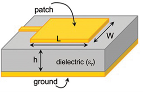
The goal of PoCat payload 3 is to identify Radio Frequency Interference (RFI) in the lower Ka-band (24-25 GHz). A patch antenna is chosen as the resonant element for its lightweight, 2D design, and reduced size due to the inverse frequency-wavelength relationship. A basic Microstrip Patch antenna consists of a conductive patch on one side of a dielectric substrate, with a ground plane on the other, emitting radiation through fringing fields at the patch edge.
Requirements and specifications
The design process is split in two main tasks. First, the single element design, includes choosing the appropriate substrate material, determine the patch antenna dimensions and the feedline that will match the patch with the rest of the array, and secondly, the design of the feeding network and the patches’ distribution.
SINGLE ELEMENT: MICROSTRIP PATCH ANTENNA
SUBSTRATE
To optimize antenna performance, the choice of substrate is crucial. A low dielectric constant (𝜀r) is preferred for minimal losses, improved efficiency, broader bandwidth, and better radiation. Increasing substrate height or reducing permittivity can also increase the bandwidth, but it may introduce undesired radiation and coupling to other components due to surface waves in the substrate. The loss tangent (tan(𝛿) or Df) is another main parameter affecting losses, with higher values indicating more dielectric absorption and losses. Rogers-5880, with a Df value of 0.0009 at 10GHz, is a suitable choice due to its low loss characteristics.
SINGLE ELEMENT DIMENSIONS
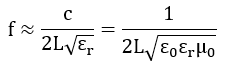
The initial patch dimensions are given by the following equation, which gives a patch side of ~4 mm using the Rogers-5880 substrate at a 24.5 GHz frequency.
The length of the patches may be changed to shift the resonances of the centre fundamental frequency of the individual patch elements. The resonant input resistance of a single patch can be decreased by increasing the width of the patch. This is acceptable if the relation between the patch width and patch length (W/L) does not exceed 2 since the aperture efficiency of a single patch begins to drop, as W/L increases beyond this value.
Patch antenna main parameters:
PATCH ANTENNA MATCHING
In this project, the chosen method is to use a microstrip line attached at the edge of the patch, combined with adding an inset into the patch itself as shown in the following figure.
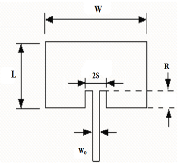
The longitude of the inset R can be calculated with the following equation where Zin(R) is the matching impedance and Zin(0) is the impedance at the edge of the patch (if the patch was fed in the end).
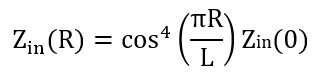
Hence, by feeding the patch antenna as shown, the input impedance can be decreased to tune it at the desired value. The spacing S is a more challenging parameter to estimate, and it requires the simulation software to define it.
2X2 PATCH ANTENNA ARRAY
The last step in the design process of a 2x2 patch antenna is to design the entire feeding network and the patches distribution. Knowing this field has been exhaustively studied, some made designs were considered at the beginning of this project, and researching about this technology, a design of a 24 GHz lineally polarized patch antenna, with the inset impedance matching technique, was found in an online repository from Zhengyu Peng, Ph.D. (Texas Tech University). In this manner, a reverse engineering study has been carried out to understand this design and then adapt it further to our requirements.
Array model and electrical lengths of the feeding network:
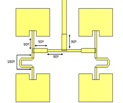
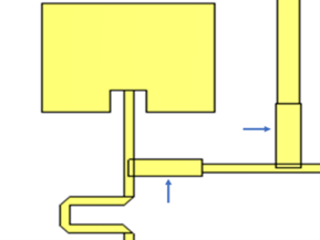
By adding an extra 180º length to access the patches from the bottom of the structure, the waves from the two resonant elements are adding up to each other. In addition, the corner mitering technique has been used as well.
Mitred bend:

A 90º bend in a transmission line adds a small amount of capacitance to the transmission line, which causes a mismatch. A mitred bend as shown in the previous figure reduces some of that capacitance, restoring the line back to its original characteristic impedance. On the other hand, the whole structure impedance matching is done by two quarter-wave impedance transformers, adjusting the trace’s width to obtain the desired characteristic impedance that sets 50 Ω at the output of the network.
λ/4 impedance transformers:
The λ/4 impedance transformer design equation is included below, where Z0 is the characteristic impedance of the line, Zin the input impedance and ZL the impedance of the load.

Each line has been designed to match this equation according to the required input and output impedance:

- Mw45: 45 (Ω)
- Mw50: 50 (Ω)
- Mw57: 57 (Ω)
- Mw81: 81 (Ω)
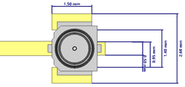
CONNECTOR
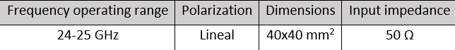
The antenna will be positioned on the upper side of the satellite. Therefore, the dimensions of the substrate layer are determined by the PoCat's own dimensions, which measure 40x40 mm². To enable the assembly of the entire structure, the payload's board includes holes for pins and screws. Additionally, a HIROSE C.FL connector is attached to the top section of the structure, where it connects to the 50 Ω feeding line. This allows easy access for the coaxial cable to connect to the upper layer from below, requiring the incorporation of a hole into the substrate and ground plane, placed at the farthest point compatible with elements from payload 2.
Connector mounting pattern following HIROSE’s recommendation:
FINAL 2X2 PATCH ANTENNA ARRAY MODEL
Data Acquisition

Parameters:
struct rfi5gParameters{
char* name;
uint32_t timestamp;
uint32_t temperature;
uint32_t startFrequency;
}
Constants
General Constants
#define N_SAMPLES 1000
#define NUM_FREQ 62
#define R 10
N_SAMPLES: Number of samples to capture in one frequency bin.
NUM_FREQ: Number of frequency bins.
R: Number of repetitions for the calibration step.
Statistical Constants
#define KU_UPPER_THRES 3.3
#define KU_LOWER_THRES 2.7
#define SK_UPPER_THRES 200
#define SK_LOWER_THRES -200
Upper and lower thresholds for kurtosis and skewness.
Notice that skewness is multiplied by 1000.
Time Domain Constants
For the time domain the threshold is defined as th = βσ + m
#define AGGRESSIVENESS_TIME 1.5
#define PERCENTAGE_TH 0.01
#define K 1.3339
AGGRESSIVENESS_TIME: Aggressiveness Time (aka β) is an empirical value obtained by simulating different INR values.
PERCENTAGE_TH: Percentage Threshold is the minimum percentage to consider the existence of an interferent signal, it is defined as the minimum number of detection out of N_SAMPLES.
Frequency Domain Constants
#define AGGRESSIVENESS_FREQ 1.5
AGGRESSIVENESS_FREQ: Aggressiveness Frequency is an empirical value obtained by simulating different INR values.
Structures Definition
typedef struct{
uint16_t mean;
uint16_t stdv;
uint16_t ku;
int16_t sk;
uint16_t Ndet;
uint8_t decision;
} tRFIbinCapture;
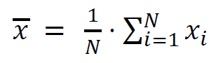
mean: Mean is a statistical parameter that shows the central tendency of the distribution.
stdv: Standard Deviation is the square root of the second standardized moment, it measures the dispersion of the distribution.
sk: Skewness, also known as the third standardized moment, is a metric that characterizes the asymmetry of the distribution.
ku: Kurtosis is the fourth standardized moment, that measures how big are the tails of the distribution.
Ndet: Number of detections counts the number of samples that had surpassed the threshold in time domain algorithm.
decision: Decision is an 8 bits variable, which flags with a pair of bits if an alogorithm has detected an interference.
From the least significant bit to the more significant bit, the flags are grouped in pairs:
-The first two bits are turned on if the statistical domain algorithm detects an interference.
-The second pair of bits are activated if the time domain algorithm detects an interference.
-The third pair of bits are activated if the frequency domain algorithm detects an interference.
-The fourth couple of bits is the combination of the previous decisions, if any algorithm has detected an interference these two bits are turned on.
Due to the possibility of ions or electromagnetic radiation to strike into the electronic circuits, causing an unwanted bit change, commonly refered as single event upset (SEU), each decision bit has a redundancy of one.
typedef struct{
uint16_t id;
tRFIbinCapture captures[NUM_FREQ];
} tRFIsweepCapture;
tRFIsweepCapture: This struct consists in the frequency axis data, since the system does not do a continuous frequency sweep, the axis is discretitzed in NUM_FREQ bins.
id: It is the identifier of a capture.
Comms considerations
As of now this section is in development
Non mandatory data:
- Frequency bins with 0 Number of Detections.
- Statistical parameters
- sweepCapture.Id (it is already identifies by timestamp)
RFI-Dedicated Thread
RFI Thread
Introduction
Like many other subsystems, the Payload is a self-contained sub-system and so it has its own FreeRTOS Thread. This thread is concieved to be able to control each of the two RFI monitoring payloads.
As an overview, the thread is structured as secuential general operations. And each of them is a key step in the process of making the payload work.
Block Diagram
To begin, the general behavior of the code is defined, since it is basic to have it structured from the most generic functions to the most specific ones. This general structure is basic since it is the one that will be in direct ”contact” with the OBC code, and its structure and functioning requirements.

This figure, as stated above, defines how the payload code is structured and its sequential steps. Note that the discontinuous arrow indicates that once the loop has finished, the payload thread enters a sleep mode, waiting for the OBC to awaken him again to restart the loop. So, the first to take a deeper look into is going to be the Check start conditions block:

As it can be seen above, the first thing to do in order to get the payload running properly is to check if the conditions required by the Ground Station user are met, this includes three things:
- The satellite is pointing at the desired region of the Earth steadily.
- The order to make an RFI measurement has been truly received.
- It is the scheduled moment to take the photo.
If none of these requirements are met, the thread awaits until it is signaled by the OBC and then rechecking everything again. Once the check has been succeed, it is time to Start the electronics and the timer:

Obviously, the first step is to power on the payload and consequently all its elements. Then the ADC and DAC are initialized and started. The same happens to the timer. Once they have been started it is time to make sure that they work as expected:

Now the ADC and DAC are checked and calibrated, the timer is only checked. This is done to assure that when using them in the measurements they don’t give false reading due to a malfunction. Having everything powered on, initialized and checked, the measure loop can begin:

This loop is run as many times as needed in order to scan all the frequency bins forming the L or Ka bands. This scans are slow, so not to block the whole satellite system, every time a frequency bin is scanned the thread checks for notifications coming from the rest of the PQ to pause itself if necessary. Then, once the satellite does not need to have the RFI thread stop anymore, the RFI thread continues from where it was.
In order to bring the explanation to a lower level, the list below explains each block step by step:
- Prepare variables: Every variable that is going to be used during the measure loop execution needs to be initialized to ensure a solid structure in the RAM (Random Access Memory).
- Configure DAC: As explained in Chapter 4.2.3, the DAC (Digital to Analog Converter) is configured to make the oscillator output a certain frequency (depending on the frequency bin that wants to be analyzed) by inputting the accordingly calculated voltage.
- Wait X ticks: a yet to be calculated amount of clock ticks is waited to ensure that the frequency from the CO (Controlled Oscillator) is stable.
- The amount of ticks needed depends on the clock speed, and DAC configuration and stabilisation time, which can be found in the microcontroller datasheet. The amount of ticks awaited must exceed an equivalent time of 7.5us.
- This calculation is done taking into account the clock speed and therefore the tick period. This results in the next formula: X = 7.5/fclk[MHz]
- Read ADC N times: The ADC reads the voltage from the RSSI output and converts it to a digital value. This is done N times for the posterior time domain analysis of the samples. The value of N is calculated by dividing the BW (Bandwidth) of the band with the RSSI BW, resulting in the next formula: N = BW/BWRSSI .
- For the L band: Since the RSSI BW is 4 MHZ, the resulting N = 250 .
- For the Ka band: Since the RSSI BW is 16 MHZ, the resulting N = 63 .
- Process Data: With the raw ADC (Analog to Digital Converter) values, calculate different statistical parameters to represent that frequency bin. Those will be stored, whereas the raw values will not.
- Store Data: Store the data mentioned before in a array that will store the statistical data from each frequency bin.
Now that the measurements have been done, it is time to power off this subsystem:

So, first both ADC and DAC are stopped, then the payload is powered off and then the timer is stopped.
To finish the thread execution, the end of the payload work is signaled to the OBC and then the thread enters sleep mode.
Detection algorithms
Temporal algorithm
The aim of this sub-algorithm is to detect pulses through Envelope Detection, a straightforward technique used for RFI monitoring. It involves sampling the input signal and comparing its power with a predetermined threshold. The detector continuously observes the power of the received signal in each temporal sample and establishes a threshold based on the typical noise floor level. When the power level of the samples exceeds this threshold, the detector interprets it as a presence of RFI.
Although the Envelope Detection algorithm has been chosen, other time domain detection algorithms exist such as the FFT (Fast Fourier Transform) based ones. FFT is the most important calculation when talking about time sampled signal processing because it allows to not only analyse the signal in the temporal domain but also in the frequency one. And by combining these two ones, advanced algorithms can be elaborated.
In addition to that, despite the very limited processing capabilities of the microcontroller used in the satellite, some advances are being done. Some preliminar tests have already proven the possibility to compute FFTs in that microcontroller. In the following weeks the integration of those algorithms with the rest of the code will be tried and tested.
Now the mathematical algorithm will be explained. First, the temporal samples vector, expressed as: 𝑥[𝑛];being N the number of samples taken Is iterated in order to calculate its mean:
Finally, if the 𝑥 is higher or lower than an arbitrary threshold the decision of whether there is in fact a signal or not is taken. This threshold is the most important part of the algorithm and its value highly affects the accuracy of the decision.
Statistical Algorithm
The purpose of this sub-algorithm is to estimate if there are signals based on their third and fourth statistical moments. These moments are extracted from the temporal samples taken in each frequency bin.
However, there are many other statistical parameters that can be taken into account, such as the standard deviation, the covariance or the correlation. Unlike the reason above, these parameters will not be used because they are not considered necessary with the given skewness and kurtosis reliability.
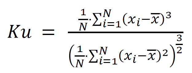
Now the kurtosis formula will be explained:

Where: 𝑥𝑖 is the i-th sample.
In the numerator of the fraction there is the calculation of the fourth statistical moment, while in the denominator there is the standard deviation elevated to the fourth power. Now the skewness formula will be explained:
Where: 𝑥𝑖 is the i-th sample.
In the numerator of the fraction there is the calculation of the third statistical moment, while in the denominator there is the standard deviation elevated to the third power.
Again, as explained in the time domain algorithm, the decision of the statistical algorithm is based on the comparison between the statistical parameters and predefined thresholds that, if exceeded or not, a decision is then made.
Frequency Algorithm
The aim of this sub-algorithm is to detect signals in the frequency domain and eventually mitigate them by frequency blanking. This technique operates in a similar manner to Envelope Detection, but in the frequency domain. If a significant increase in power is observed at a particular frequency bin compared to its neighbouring bins, it may indicate the presence of interference. These power peaks are more easily detected when they have high power in a narrow bandwidth.
This analysis is done by comparing the received power from adjacent frequencies and applying a threshold to distinguish these values. So, if the algorithm detects a signal that is above that threshold, it decides that it is in fact an Interference.
Test
RFI-5G FE-Bottom SSV
Test Description and Objectives
The objective of this test is to validate the correct operations of the P/L2 K-band RFI monitoring payload board layout, the quality of the data acquisition process, as well as the deployment and operation metrics of the Helical antenna. This test is meant to be performed both upon each new board assembly, as many of the errors discovered with this test are manufacturing-related and thus repeatable, as well as after any environmental test on the same board.
Requirements Verification
| ID | Description | Status |
|---|---|---|
| M-0700 | The L-band receiver antenna will be omnidirectional, operate in the 1-2 GHz band and feature a reflection coefficient greater than 6 dBs. | Ok |
| M-0710 | The L-band receiver antenna will be contained inside the satellite's allowed space envelope during launch and capable and controlled deployment once in orbit | TBC |
| M-0720 | The L-band receiver front end will be compatible with the rest of the satellite in terms of power requirements and data exchange and storage capabilities. | TBC |
| M-0730 | The L-band receiver front end will attain a 5 MHz or better frequency resolution. | TBC |
This specifications should be further detailed? To clarify the SSV results
Test Set-Up
For performing this test, the following items are required:
- completely soldered P/L3 boards.
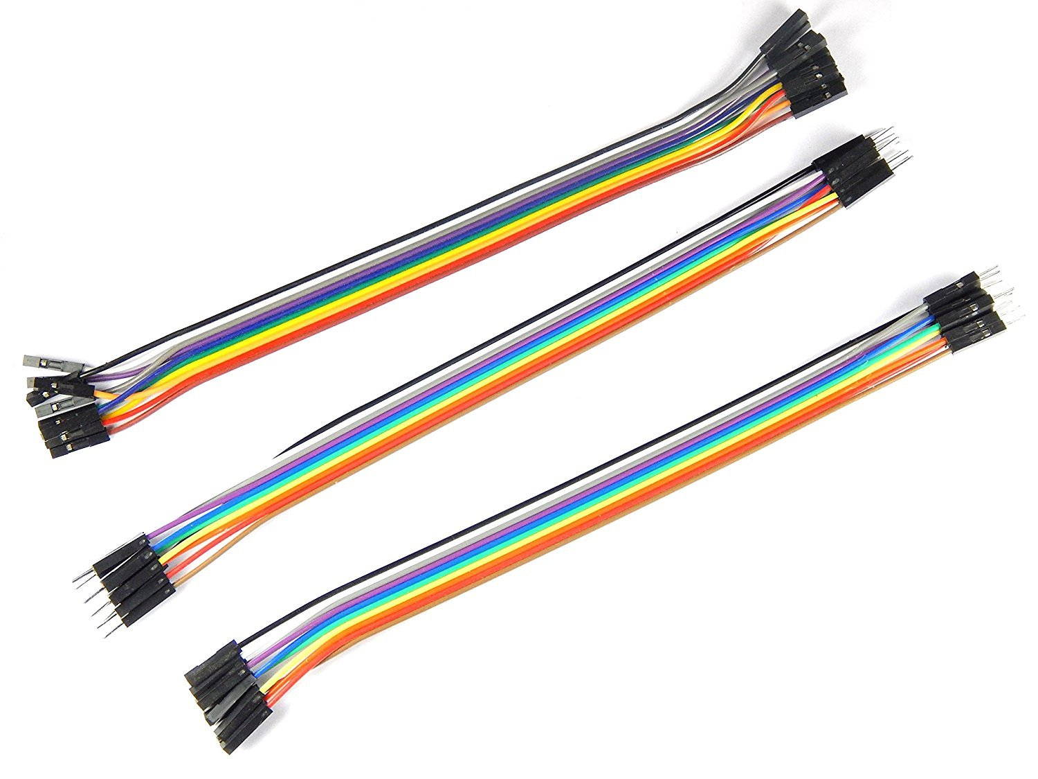
- 9 male to female jumper cables
- 1 pin oscillocope probe
- 2 banana-banana power cables
- 1 multimeter with sharp termination cables
- 1 power supply
- 1 Signal generator (10 MHz - 8 GHz)
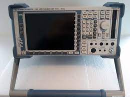
- 1 Spectrum Analyser (up to 25 GHz)
- 1 SMA DC block
- 2 SMA to SMA 50 ohm coaxial cables
- 2 SMA to U.FL header transition
- 2 SMA to MS156 probe transition
- 1 OBC board with at least the STM and pull up resistors soldered OR a Nucleo board + PC with SMT32Cube IDE + USB to mini USB cable
Below is the connections schematic:
Make connections
- Turn on equipment
- Spectrum analizer
- Signal generator
- Power supply
-
Configure to desired parameters
- Spectrum analizer
- Set center frequency
- Set enough span
- Set RBW and VBW to an adecuate level
- Power supply
- Set Voltage to 3.3V
- Set current limit to 0.3A
- Spectrum analizer
-
Set up nucleo board and PC
- Make sure the proper code is loaded into the nucleo board
- Connect the power supply to the payload:
- Vcc to PoL
- GND to GND
- Connect the DAC output to the DAC 1
- Connect the ADC input to the ADC_Out
- Connect the signal generator output to the IF input PIN
- Connect the spectrum analizer to the switched measuring pin
- Connect PC to ground (plug in the charger).
- Connect necleo board to computer by USB.
Pass/Fail Criteria
This test will be considered passed if all of the following actions are performed succesfully:
- The code executes correctly upon flashing.
- A 1 GHz band noise-level sweep centered at 24.5 GHz is correctly filtered, amplified, downconverted to 869 Mhz within a 16 MHz bandwidth at -6dB.
- The resulted signal is translated by the RSSI into the appropiate voltage according to the manufacturer's specifications.
- The data aquisition process is correctly performed with the data being accessible from the STM32's flash memory banks.
- The system detects correctly certain RF signalssed detection is yet to be completely characterized.
The signals inputed and their supposed detection is yet to be completely characterized.
Test Plan (By Subblocks)
Before moving towards the testing of the whole subsystem, in order to single out possible errors, the payload's isolated segments will be tested a part, starting for simplicity with those which do not require a STM32 (be it a Nucleo Board or the OBC&COMMS board) to be verified.
RF chain Low Noise Amplifier (LNA)
In the form of the HMC342, fully explained in the appropiate P/L page, under the ³Cat-NXT Design chapter, the LNA is supposed to provide a gain of arround 19dB (at 24-25 GHz) over the Ka-band. To test this feature, a signal will be introduced at the receiver's input, and sampled from the first RF chain probe. The procedure is as follows:
-
First of all, the board should be operational. This can be checked by having a current consumption of cca 230 mA seen on the power supply display and with a voltage between 3.1 V and 3.3 V measured between the P/L_Power and GND pins. If otherwise, repeat the previous sub-section steps.
-
Connect the signal generator output through the SMA-U.FL termination to the J1 coaxial header input connector.
-
Attach pin probe termination to the free end of the coaxial cable of the spectrum analyser and connect it to the output pin of the LNA.
-
Set up the spectrum analyser to a center frequency of 24.5 GHz, a span of 2 GHz (having a total observable window from 23.5 GHz to 25.5 GHz) and using the maxim Autopick setting for ease of interpretation.
-
With the board and LNA powered as detailed above, select a tone of -80 dBm in ampltude and 24.5 GHz of frequency on the signal generator and then enable its output.
-
Observe the reading on the spectrum analyser. The same tone inputted should be visible, but with an amplitude gain of cca 19 dB. Note down any frequency shift if the case and take screen captures as needed.
-
Repeat the last two steps, this time at a number of different frequencies from 24 GHz to 25 GHz. It is recommended to do so at 100 MHz apart.
-
If the gain observed along said measurements coincides with the values provided by the manufacturer within a 5% tolerance, this test is considered passed.
Bandpass filters
Once the LNA is proven to work fine, the filters mut be checked. For these operations the same procedure is followed.
-
Connect a 50 Ohm matching load to the SMA-U.FL termination to the J1 coaxial header input connector, the RF Input.
-
Attach a pin probe termination to the free end of the coaxial cable of the spectrum analyser and connect it to the output pin of the filter.
-
This step is detailed for each filter.
-
If the BW observed along said measurements coincides with the values provided by the manufacturer within a 5% tolerance, this test is considered passed.
Ka band filter
-
Set up the spectrum analyser to a center frequency of 24.5 GHz, a span of 2 GHz (having a total observable window from 23.5 GHz to 25.5 GHz).
- Meaure the observed BW at -3dB.
IF filtering
-
Set up the spectrum analyser to a center frequency of 7169 MHz, a span of 2 GHz.
- Meaure the observed BW at -3dB.
SAW filter
The B39871B4316P810 bandpass filter's function is to select the signal within a range indicated by the manufacturer to be between 862 MHz and 876MHz, with an insertion loss of lower than 1.6 dB in-band. These characteristics can be tested as follows:
-
Set up the spectrum analyser to a center frequency of 869 MHz, a span of 50 GHz.
- Meaure the observed BW at -3dB.
RF downconversion tuner
The downconversion of this receiver is done using the voltage controlled HMC260 tuner, from the 24-25 GHz RF chain to the 7 GHz IF chain, by applying a frequency sweep. The steps to follow are:
-
Make sure that the configuration from the Set-Up section is in place.
-
Verify that the OBC PoL is turned on and the DAC pin holds a voltage constant controllable voltage.
-
Connect the signal generator output through the SMA-U.FL termination to the J1 coaxial header input connector.
-
Attach a SMA-U.FL probe termination to the free end of the coaxial cable of the spectrum analyser and connect it to the J2 U.FL coaxial header, the IF input terminal.
-
Set up the spectrum analyser to a center frequency of 24.5 GHz, a span of 2 GHz (having a total observable window from 23.5 GHz to 25.5 GHz) and using the maxim Autopick setting for ease of interpretation.
-
With the board powered as detailed above, select a tone of -80 dBm in ampltude and 24.5 GHz of frequency on the signal generator and then enable its output.
-
Observe the reading on the spectrum analyser. The same tone inputted should be visible, but with an amplitude loss of 9 to 12 dB. More importantly, the frequency shift must be the one according to the inputed voltage.
Note that the relation between voltage and frequency is not linear and need to be characterized as stated in the VCO calibration procedure
-
Repeat the last two steps, this time at a number of different frequencies from 24 GHz to 25 GHz. It is recommended to do so at 100 MHz apart.
-
If the attenuation and frequency shift observed along said measurements coincides with the values provided by the manufacturer within a 5% tolerance, this test is considered passed.
IF downconversion tuner
The downconversion of this receiver is done using the voltage controlled SIM-14+ tuner, from the 6669-7669 MHz IF chain to the 869 MHz LF chain, by applying a frequency sweep. The steps to follow are:
-
Make sure that the configuration from the Set-Up section is in place.
-
Verify that the OBC PoL is turned on and the DAC pin holds a voltage constant controllable voltage.
-
Connect the signal generator output through the SMA-U.FL termination to the J1 coaxial header input connector.
-
Attach a SMA-U.FL probe termination to the free end of the coaxial cable of the spectrum analyser and connect it to the J3 U.FL coaxial header, the IF input terminal.
-
Set up the spectrum analyser to a center frequency of 7169 MHz, a span of 2 GHz, and using the maxim Autopick setting for ease of interpretation.
-
With the board powered as detailed above, select a tone of -80 dBm in ampltude and 7169 MHz of frequency on the signal generator and then enable its output.
-
Observe the reading on the spectrum analyser. The same tone inputted should be visible, but with an amplitude loss of 6.7 to 9.5 dB. More importantly, the frequency shift must be the one according to the inputed voltage.
Note that the relation between voltage and frequency is not linear and need to be characterized as stated in the VCO calibration procedure
-
Repeat the last two steps, this time at a number of different frequencies from 24 GHz to 25 GHz. It is recommended to do so at 100 MHz apart.
- Repeat the last three steps, this time at a number of different VCO voltages from 0 to 3 V. It is recommended to do so at 100mV apart.
-
If the attenuation and frequency shift observed along said measurements coincides with the values provided by the manufacturer within a 5% tolerance, this test is considered passed.
Test Plan (Full subsystem)
From this point the document is a stub.
Having tested and isolated possible errors as much as possible in a bit-by-bit manner in the previous section, a full subsystem test will now be performed.
-
Make sure that the configuration from the Set-Up section is in place as well as the OBC PoL is turned on.
-
Connect the signal generator output through the SMA-U.FL termination to the J1 coaxial header. It is recommended that at least the first full SSV is done by way of signal generator input, with later tests possibly replacing this input with the real one by way of the antenna in order to firstly test the front end separate from any possible errors.
-
Configure the signal generator to output a 24 GHz - 25 GHz frequency sweep of -100 dBm amplitude with random spikes at -80 dBm and enable its output.
-
Using the IDE, initiate the P/L task within the STM32, using the full PQ firmware scheduler.
-
Using the Umbilical connection, download the flash memory experiment files
7. Test Results
8. Anomalies
9. Conclusions
RFI-5G FE-Top SSV
Document Scope
The objective of this document is to detail the procedures, results and conclusions to properly test at subsystem level the RFI-5G front-end top board. Several parts will be tested:
- Test of the LNA chain
- Test of the LO chain
- Test of the Front-End top board RF
- Test of the temperature sensor
Test of the LNA chain
Test Description and Objectives
The purpose of this test is to validate that the HMC342 LNA amplifier provides the expected +19 dB of gain for input signals between 24 to 25 GHz, and that the band-pass filter does not introduce more than the expected -4 dB of losses.
Since the probing used is not the frequency range used, this is only a qualitative test to check if the LNA is providing gain and validate that the consumption is nominal.
Requirements Verification
This test does not verify any requirement, and is only to check that the board part works as expected.
Test Set-Up
The required components for this test are the following:
| RFI-5G front-end top board |
|
| C.FL to SMA-2.92mm adapter |
|
| C.FL cable |
|
| RF probe |
|
| SMA 50 Ohm RF load |
|
| DC Block N to SMA adapter |
|
| Power supply |
|
| Signal Generator capable of at least 25 GHz |
|
| Spectrum Analyzer capable of at least 25 GHz |
|
| 2x Jumper cables |
|
| 2x Banana cables |
|
| 2x Crocodrile clips |
|
| 2x SMA 2.92 mm cables |
|
| SMA to SMP cable |
|


The steps to prepare the setup are the following:
- Connect the output from the signal generator to the antenna input of the RFI-5G front-end top board by using the C.FL cable and the C.FL to 2.92 mm adapter.
- Connect the power supply to the Vcc_LNA1 and GND pins with the jumper cables and the crocodile clips.
- Connect the DC-block N to SMA adapter to the spectrum analyzer input.
- Connect the RF probe to the spectrum analyzer using one SMA cable.
- Connect the SMA 50 Ohm RF load to the output of the mixer with the SMA to SMP cable.
The diagram below represents the initial setup:

Pass/Fail Criteria
The test will be considered successful if the LNA shows to provide gain (~19 dB) and the power consumption matches the expected one (~43 mA at 3.3 V). There is though some margin accepted, since the RF probe and cables are not rated for the frequency range used.
Test Plan
|
Step ID |
Description |
Pass/Fail Criteria |
Actual |
Passed [Y/N] |
| RFI-5G-TOP-LNA-000 |
Make sure that the power supply and signal generator outputs are off. | Passes if power supply and signal generator outputs are off. |
||
| RFI-5G-TOP-LNA-010 |
Prepare the setup as stated in 2.3. |
Passes if setup prepared. |
||
| RFI-5G-TOP-LNA-020 |
Set the power supply to 3 V and limit the current to 60 mA. |
Passes if power supply set. |
||
| RFI-5G-TOP-LNA-030 |
Set the signal generator to: f = 24.5 GHz Pout = -70 dBm |
Passes if signal generator set. |
||
| RFI-5G-TOP-LNA-040 |
Set the spectrum analyzer to: f = 24.5 GHz Span = 10 MHz RBW = 10 kHz VBW = 1 kHz Trace = Max Hold |
Passes if spectrum analyzer set. |
||
| RFI-5G-TOP-LNA-050 |
Switch on the signal generator output. |
Passes if signal generator output is on. |
||
| RFI-5G-TOP-LNA-060 |
Switch on the power supply. If the power supply is limiting switch it off immediately. |
Passes if power supply is on and not current limiting. |
||
| RFI-5G-TOP-LNA-070 |
Note the voltage and current. If the current consumption is abnormal switch it off immediately. |
Passes if voltage and current are within specification (some margin is allowed but has to be explained why). |
Voltage: Current: |
|
| RFI-5G-TOP-LNA-080 |
With the RF probe, probe the input of the LNA by carefully touching with the signal pogo-pin the RF input pin of the LNA. |
Passes if a signal is shown in the spectrum analyzer. |
||
| RFI-5G-TOP-LNA-090 | Set the trace mode in the spectrum analyzer to VIEW to freeze the image. |
Passes if trace mode is VIEW. |
||
|
RFI-5G-TOP-LNA-100 |
Add a second trace in the spectrum analyzer with the same configuration as the first one. |
Passes if spectrum analyzer set. |
||
| RFI-5G-TOP-LNA-110 | With the RF probe, probe the output of the LNA by carefully touching with the signal pogo-pin the RF output pin of the LNA. |
Passes if a signal is shown in the spectrum analyzer. | ||
| RFI-5G-TOP-LNA-120 | Set the trace mode in the spectrum analyzer to VIEW to freeze the image. |
Passes if trace mode is VIEW. |
||
| RFI-5G-TOP-LNA-130 |
Add one marker to the peak of trace 1, and another marker that measures the delta in the peak of trace 2. Note the gain and frequency delta values. |
Passes if the gain is within specification (some margin is allowed but has to be explained why). |
Gain: Frequency: |
|
| RFI-5G-TOP-LNA-140 |
Capture the screen of the spectrum analyzer and save it into a USB drive. |
Passes if .wmf is saved into a USB drive. |
File name: |
|
| RFI-5G-TOP-LNA-150 |
Add a third trace in the spectrum analyzer with the same configuration as the first one. |
Passes if spectrum analyzer set. |
||
| RFI-5G-TOP-LNA-160 | With the RF probe, probe the output of the band-pass filter by carefully touching with the signal pogo-pin the RF output pin of the filter. | Passes if the gain is within specification (some margin is allowed but has to be explained why). | ||
| RFI-5G-TOP-LNA-170 | Set the trace mode in the spectrum analyzer to VIEW to freeze the image. |
Passes if trace mode is VIEW. |
||
| RFI-5G-TOP-LNA-180 |
Add a third marker in trace 3. Note the power and frequency delta values with marker 1. |
Passes if the gain is within specification (some margin is allowed but has to be explained why). |
Gain: Frequency: |
|
| RFI-5G-TOP-LNA-190 |
Capture the screen of the spectrum analyzer and save it into a USB drive. |
Passes if .wmf is saved into a USB drive. |
File name: |
|
| RFI-5G-TOP-LNA-200 |
Switch off the power supply and the signal generator. |
Passes if power supply and signal generator are off. |
||
| RFI-5G-TOP-LNA-210 |
If all steps are passed, proceed with next test. |
Passes if all steps passed. |
Test Results
Description of the Test results with supporting data.
- Test name, test execution dates, the test facility used and the operators
- Test Logbooks
- “As-run” procedures (to be provided in annex)
- Test facility results (if applicable)
- Photographs relevant to the set-up(s) and inspection(s) (may also be added in the Conclusions to clarify a close-out judgement, e.g. for an inspection)
- Analysis of the test data and relevant assessment.
- Synthesis of the overall test results per verification (e.g. Vibration, Inspection 1, Inspection 2, etc.).
Anomalies
List of deviations to the Test Specification and Procedure and non-conformances witnessed during the test campaign, including a brief description, the close-out status and reference to the relevant reports.
Conclusions
The Conclusions shall include (where needed as annex):
- Test results, including as a minimum:
- Requirement to be verified
- Subsections of test campaign in which that requirement was verified (e.g. Thermal Vacuum RFT 1, Inspection 1, Inspection 2, ...)
- Close-out judgement (compliance status) and rationale, per subsection of the test
- Traceability to used documentation
- Conformance or deviation including references
- Overall conclusion on the success of the test, including clearly stated and described open issues and possible remediating actions.
- Test Readiness Review minutes and Post Test Review minutes
Test of the LO chain
Test Description and Objectives
The purpose of this test is to validate that the LO chain works as intended. This means that the HMC506 VCO provides a tone at the expected 8665.5 MHz, and that the HMC342 LO amplifier provides gain (~19 dB) so that the LO input of the mixer is over 12 dBm (~14 dBm).
Since the probing used is not the frequency range used, this is only a qualitative test to check if the LO chain is providing the correct LO tone to the mixer and that the consumption is nominal.
Requirements Verification
This test does not verify any requirement, and is only to check that the board part works as expected.
Test Set-Up
The required components for this test are the following:
| RFI-5G front-end top board |
|
| C.FL to SMA-2.92mm adapter |
|
| C.FL cable |
|
| RF probe |
|
| SMA 50 Ohm RF load |
|
| DC Block N to SMA adapter |
|
| Power supply |
|
| Spectrum Analyzer capable of at least 25 GHz |
|
| 6x Jumper cables |
|
| 6x Banana cables |
|
| 6x Crocodrile clips |
|
| 2x SMA 2.92 mm cables |
|
| SMA to SMP cable |
|
The steps to prepare the setup are the following:
- Connect the output from the signal generator to the antenna input of the RFI-5G front-end top board by using the C.FL cable and the C.FL to 2.92 mm adapter.
- Connect the first channel of the power supply to the Vcc_VCO and GND pins with the jumper cables and the crocodile clips.
- Connect the second channel of the power supply to the Vtune1 and GND pins with the jumper cables and the crocodile clips.
-
Connect the third channel of the power supply to the
and GND pins with the jumper cables and the crocodile clips.Vcc_IF1AmpVcc_LO1Amp - Connect the DC-block N to SMA adapter to the spectrum analyzer input.
- Connect the RF probe to the spectrum analyzer using one SMA cable.
- Connect the SMA 50 Ohm RF load to the output of the mixer with the SMA to SMP cable.
The diagram below represents the initial setup:

Pass/Fail Criteria
The test will be considered successful if the LO shows a tone at 8665.5 MHz +- 5%, if the LO amplifier provides the expected gain (~19 dB) and if the level of the LO input of the mixer is over 10 dBm. Additionally, the current consumption has to be nominal.
Test Plan
|
Step ID |
Description |
Pass/Fail Criteria |
Actual |
Passed [Y/N] |
| RFI-5G-TOP-LO-000 |
Make sure that the power supply is off. |
Passes if power supply and signal generator outputs are off. |
||
| RFI-5G-TOP-LO-010 |
Prepare the setup as stated in 3.3. |
Passes if setup prepared. |
||
| RFI-5G-TOP-LO-020 |
Set the first channel of the power supply to 3 V and limit the current to 100 mA. |
Passes if power supply set. |
||
| RFI-5G-TOP-LO-030 |
Set the second channel of the power supply to 8.7 V and limit the current to 10 mA. |
Passes if power supply set. |
||
| RFI-5G-TOP-LO-040 | Set the third channel of the power supply to 3 V and limit the current to 60 mA. |
Passes if power supply set. |
||
| RFI-5G-TOP-LO-050 |
Set the spectrum analyzer to: f = 8665.5 MHz Span = 100 MHz RBW = 100 kHz VBW = 3 kHz Trace = Clear/Write |
Passes if spectrum analyzer set. |
||
| RFI-5G-TOP-LO-060 |
Switch on the first channel of the power supply. If the power supply is limiting switch it off immediately. |
Passes if power supply is on and not current limiting. |
||
| RFI-5G-TOP-LO-070 |
Switch on the |
Passes if power supply is on and not current limiting. |
||
| RFI-5G-TOP-LO-080 |
Note the voltage and current. If the current consumption is abnormal switch it off immediately. |
Passes if voltage and current are within specification (some margin is allowed but has to be explained why) |
CH1 Voltage: Current: CH2 Voltage: Current: |
|
| RFI-5G-TOP-LO-080 |
With the RF probe, probe the output of the VCO by carefully touching with the signal pogo-pin the RF output pin of the LNA. |
Passes if a signal is shown in the spectrum analyzer. |
||
| RFI-5G-TOP-LO-090 | Adjust the Vtune1 voltage until the LO frequency is centered to the desired 8665.5 MHz. |
Passes if LO frequency is ~8665.5 MHz. |
CH2 Voltage: frequency: |
|
| RFI-5G-TOP-LO-100 | Set the trace mode in the spectrum analyzer to VIEW to freeze the image. |
Passes if trace mode is VIEW. |
||
| RFI-5G-TOP-LO-110 | Capture the screen of the spectrum analyzer and save it into a USB drive. |
Passes if .wmf is saved into a USB drive. |
File name: |
|
| RFI-5G-TOP-LO-120 | Set the trace mode in the spectrum analyzer to CLEAR/WRITE to clear the spectrum. |
Passes if trace mode is CLEAR/WRITE. | ||
|
RFI-5G-TOP-LO-130 |
Set the spectrum analyzer to: f = 17331 MHz Span = 200 MHz RBW = 100 kHz VBW = 3 kHz Reference level = 10 dBm Trace = Max Hold |
Passes if spectrum analyzer set. |
||
| RFI-5G-TOP-LO-140 | With the RF probe, probe the output of the frequency multiplier by carefully touching with the signal pogo-pin the RF output pin of the frequency multiplier. |
Passes if a signal is shown in the spectrum analyzer. | ||
| RFI-5G-TOP-LO-150 | Set the trace mode in the spectrum analyzer to VIEW to freeze the image. |
Passes if trace mode is VIEW. |
||
| RFI-5G-TOP-LO-160 |
Add one marker at the peak. Note the power and frequency values. | Passes if power and frequency are within specification. |
Power: Frequency: |
|
| RFI-5G-TOP-LO-170 |
Add a second trace in the spectrum analyzer with the same configuration as the first one. | Passes if spectrum analyzer set. | ||
| RFI-5G-TOP-LO-180 |
Switch on the third channel of the power supply. If the power supply is limiting switch it off immediately. |
Passes if power supply is on and not current limiting. |
||
| RFI-5G-TOP-LO-190 | Note the voltage and current. If the current consumption is abnormal switch it off immediately. |
Passes if voltage and current are within specification (some margin is allowed but has to be explained why) |
CH3 Voltage: Current: |
|
| RFI-5G-TOP-LO-200 |
With the RF probe, probe the output of the LO amplifier by carefully touching with the signal pogo-pin the RF output pin of the LO amplifier. |
Passes if a signal is shown in the spectrum analyzer. | ||
| RFI-5G-TOP-LO-210 | Set the trace mode in the spectrum analyzer to VIEW to freeze the image. |
Passes if trace mode is VIEW. |
||
| RFI-5G-TOP-LO-220 | Add one marker to the peak of trace 1, and another marker that measures the delta in the peak of trace 2. Note the power and frequency delta values. |
Passes if the gain is within specification (some margin is allowed but has to be explained why). |
Power: Frequency: |
|
| RFI-5G-TOP-LO-230 | Capture the screen of the spectrum analyzer and save it into a USB drive. |
Passes if .wmf is saved into a USB drive. |
File name: |
|
| RFI-5G-TOP-LO-240 | Switch off the power supply and the signal generator. |
Passes if power supply and signal generator are off. |
||
| RFI-5G-TOP-LO-250 | If all steps are passed, proceed with next test. |
Passes if all steps passed. |
Test Results
Description of the Test results with supporting data.
- Test name, test execution dates, the test facility used and the operators
- Test Logbooks
- “As-run” procedures (to be provided in annex)
- Test facility results (if applicable)
- Photographs relevant to the set-up(s) and inspection(s) (may also be added in the Conclusions to clarify a close-out judgement, e.g. for an inspection)
- Analysis of the test data and relevant assessment.
- Synthesis of the overall test results per verification (e.g. Vibration, Inspection 1, Inspection 2, etc.).
Anomalies
List of deviations to the Test Specification and Procedure and non-conformances witnessed during the test campaign, including a brief description, the close-out status and reference to the relevant reports.
Conclusions
The Conclusions shall include (where needed as annex):
- Test results, including as a minimum:
- Requirement to be verified
- Subsections of test campaign in which that requirement was verified (e.g. Thermal Vacuum RFT 1, Inspection 1, Inspection 2, ...)
- Close-out judgement (compliance status) and rationale, per subsection of the test
- Traceability to used documentation
- Conformance or deviation including references
- Overall conclusion on the success of the test, including clearly stated and described open issues and possible remediating actions.
- Test Readiness Review minutes and Post Test Review minutes
Test of the Front-end Top board RF
Test Description and Objectives
The purpose of this test is to validate the correct functioning of the RF part of the RFI-5G front-end top, i.e., with an input signal between 24-25 GHz, the signal is down-converted to an intermediate signal with frequency between 6669-76669 MHz, with a net gain of 5 dB.
Requirements Verification
This test does not verify any requirement, and is only to check that the board part works as expected.
Test Set-Up
The required components for this test are the following:
| RFI-5G front-end top board |
|
| RFI-5G interface board with inverse connectors |
|
| C.FL to SMA-2.92mm adapter |
|
| C.FL cable |
|
| DC Block N to SMA adapter |
|
| Power supply |
|
| Signal Generator capable of at least 25 GHz |
|
| Spectrum Analyzer capable of at least 25 GHz |
|
| 2x Banana cables |
|
| SMA 2.92 mm cables |
|
| SMA to SMP cable |
|
The steps to prepare the setup are the following:
- Mate the RFI-5G front-end top board with the RFI-5G interface board that has the inverse pin header.
- Connect the EGSE to the power supply with the banana cables.
- Connect the output from the signal generator to the antenna input of the RFI-5G front-end top board by using the C.FL cable and the C.FL to 2.92 mm adapter.
- Connect the DC-block N to SMA adapter to the spectrum analyzer input.
- Connect the RFI-5G front-end top board output to the spectrum analyzer using the SMA to SMP cable.
The diagram below represents the initial setup:

Pass/Fail Criteria
The test will be considered successful if the output of the RFI-5G front-end top board is a signal between 6669-7669 MHz when the antenna input is between 24-25 GHz, and the board provides a net gain of +5 dB. Additionally, the current consumption has to be nominal.
Test Plan
|
Step ID |
Description |
Pass/Fail Criteria |
Actual |
Passed [Y/N] |
| RFI-5G-TOP-RF-000 |
Make sure that the power supply and signal generator outputs are off. | Passes if power supply and signal generator outputs are off. |
||
| RFI-5G-TOP-RF-010 |
Prepare the setup as stated in 4.3. |
Passes if setup prepared. |
||
| RFI-5G-TOP-RF-020 |
Set the first channel of the power supply to 3.3 V and limit the current to 200 mA. |
Passes if power supply set. |
||
| RFI-5G-TOP-RF-030 |
Set the spectrum analyzer to: f = 7169 MHz Span = 200 MHz RBW = 100 kHz VBW = 3 kHz Reference level = -20 dBm Trace = Clear/Write |
Passes if spectrum analyzer set. |
||
| RFI-5G-TOP-RF-040 |
Set the signal generator to: f = 24.5 GHz Pout = -80 dBm |
Passes if signal generator set. | ||
| RFI-5G-TOP-RF-050 |
Switch on the first channel of the power supply. If the power supply is limiting switch it off immediately. |
Passes if power supply is on and not current limiting. |
||
| RFI-5G-TOP-RF-060 | Note the voltage and current. If the current consumption is abnormal switch it off immediately. |
Passes if voltage and current are within specification (some margin is allowed but has to be explained why). |
Voltage: Current: |
|
| RFI-5G-TOP-RF-070 | Enable the output of the signal generator. | Passes if signal generator output is enabled. | ||
| RFI-5G-TOP-RF-080 | Note the voltage and current. If the current consumption is abnormal switch it off immediately. |
Passes if voltage and current are same as in RFI-5G-TOP-RF-060. |
Voltage: Current: |
|
| RFI-5G-TOP-RF-090 | Add one marker at the peak. Note the frequency and power of the intermediate signal. Additionally compute the net gain and the frequency shift. | Passes if the net gain is +5 dB and the frequency shift of 17331 MHz. |
frequency = Power = frequency shift = Gain = |
|
| RFI-5G-TOP-RF-100 | Set the trace mode in the spectrum analyzer to VIEW to freeze the image. |
Passes if trace mode is VIEW. |
||
| RFI-5G-TOP-RF-110 | Capture the screen of the spectrum analyzer and save it into a USB drive. |
Passes if .wmf is saved into a USB drive. |
File name: |
|
| RFI-5G-TOP-RF-120 | Set the trace mode in the spectrum analyzer to CLEAR/WRITE to clear the spectrum. |
Passes if trace mode is CLEAR/WRITE. | ||
| RFI-5G-TOP-RF-130 |
Switch off the output of the signal generator. |
Passes if signal generator output is off. |
||
| RFI-5G-TOP-RF-140 |
Set the spectrum analyzer to: f = 7169 MHz Span = 1200 MHz RBW = 300 kHz VBW = 30 kHz Trace = Max Hold |
Passes if spectrum analyzer set. |
||
| RFI-5G-TOP-RF-150 |
Set the signal generator to: Mode = frequency sweep f = 24.5 GHz Span = 1 GHz Step = 10 MHz P = -80 dBm |
Passes if signal generator set. |
|
|
| RFI-5G-TOP-RF-160 |
Switch on the output of the signal generator. |
Passes if signal generator output is on. |
||
| RFI-5G-TOP-RF-170 | Wait until a complete frequency sweep is done. | Passes when complete frequency sweep finishes. | ||
| RFI-5G-TOP-RF-180 | Check qualitatively the flatness of the RFI-5G front-end top board RF output. | Passes if the RF output is "flat". | ||
| RFI-5G-TOP-RF-190 | Set the trace mode in the spectrum analyzer to VIEW to freeze the image. |
Passes if trace mode is VIEW. |
|
|
| RFI-5G-TOP-RF-200 | Capture the screen of the spectrum analyzer and save it into a USB drive. |
Passes if .wmf is saved into a USB drive. |
File name: |
|
| RFI-5G-TOP-RF-210 | Switch off the power supply and the signal generator. |
Passes if power supply and signal generator are off. |
||
| RFI-5G-TOP-RF-220 | If all steps are passed, proceed with next test. |
Passes if all steps passed. |
Test Results
Description of the Test results with supporting data.
- Test name, test execution dates, the test facility used and the operators
- Test Logbooks
- “As-run” procedures (to be provided in annex)
- Test facility results (if applicable)
- Photographs relevant to the set-up(s) and inspection(s) (may also be added in the Conclusions to clarify a close-out judgement, e.g. for an inspection)
- Analysis of the test data and relevant assessment.
- Synthesis of the overall test results per verification (e.g. Vibration, Inspection 1, Inspection 2, etc.).
Anomalies
List of deviations to the Test Specification and Procedure and non-conformances witnessed during the test campaign, including a brief description, the close-out status and reference to the relevant reports.
Conclusions
The Conclusions shall include (where needed as annex):
- Test results, including as a minimum:
- Requirement to be verified
- Subsections of test campaign in which that requirement was verified (e.g. Thermal Vacuum RFT 1, Inspection 1, Inspection 2, ...)
- Close-out judgement (compliance status) and rationale, per subsection of the test
- Traceability to used documentation
- Conformance or deviation including references
- Overall conclusion on the success of the test, including clearly stated and described open issues and possible remediating actions.
- Test Readiness Review minutes and Post Test Review minutes
Test of the temperature sensor
Test Description and Objectives
The purpose of this test is to validate the correct functioning of temperature sensor in the RFI-5G front-end top board, and that the sensor library code functions correctly.
Requirements Verification
This test does not verify any requirement, and is only to check that the board part works as expected.
Test Set-Up
The required components for this test are the following:
| RFI-5G front-end top board |
|
| RFI-5G interface board with inverse connectors |
|
| RFI-5G EGSE |
|
| STM32 Nucleo-L476RG board |
|
| USB A-to-mini cable |
|
| Power supply |
|
| 2x Banana cables |
|
| 2x Jumper cables |
|
| Temperature sensor test code |
NA |


The steps to prepare the setup are the following:
- Mate the RFI-5G front-end top board with the RFI-5G interface board that has the inverse pin header.
- Connect the EGSE to the power supply with the banana cables.
- Connect the output from the signal generator to the antenna input of the RFI-5G front-end top board by using the C.FL cable and the C.FL to 2.92 mm adapter.
- Connect the DC-block N to SMA adapter to the spectrum analyzer input.
- Connect the RFI-5G front-end top board output to the spectrum analyzer using the SMA to SMP cable.
The diagram below represents the initial setup:
Missing setup picture
Pass/Fail Criteria
Description of which metric is used to perform the test and when it is considered that the test passed or not. If different metrics are used, it is important to define when the test passed or not (e.g. when all the metrics are in the pass criteria, or when only one of them).
Test Plan
This section includes the test sequence necesary to do the test. The test sequence must include all the steps, from the set-up up to the conclusion of the test.
Test Results
Description of the Test results with supporting data.
- Test name, test execution dates, the test facility used and the operators
- Test Logbooks
- “As-run” procedures (to be provided in annex)
- Test facility results (if applicable)
- Photographs relevant to the set-up(s) and inspection(s) (may also be added in the Conclusions to clarify a close-out judgement, e.g. for an inspection)
- Analysis of the test data and relevant assessment.
- Synthesis of the overall test results per verification (e.g. Vibration, Inspection 1, Inspection 2, etc.).
Anomalies
List of deviations to the Test Specification and Procedure and non-conformances witnessed during the test campaign, including a brief description, the close-out status and reference to the relevant reports.
Conclusions
The Conclusions shall include (where needed as annex):
- Test results, including as a minimum:
- Requirement to be verified
- Subsections of test campaign in which that requirement was verified (e.g. Thermal Vacuum RFT 1, Inspection 1, Inspection 2, ...)
- Close-out judgement (compliance status) and rationale, per subsection of the test
- Traceability to used documentation
- Conformance or deviation including references
- Overall conclusion on the success of the test, including clearly stated and described open issues and possible remediating actions.
- Test Readiness Review minutes and Post Test Review minutes
K-Band VCO Calibration Procedure
Objective
Measure the frequency response of the VCO and characterize it.
Steps to follow
-
Turn on equipment
- Spectrum analizer
- Power supply
-
Configure to desired parameters
- Spectrum analizer
- Set center frequency in the middle of VCO output band (6250MHz)
- Set span to match the VCO output band (1400MHz)
- Set RBW and VBW to an adecuate level
- Power supply
- Set Voltage to 3.3V
- Set current limit to 0.3A
- Spectrum analizer
-
Set up nucleo board and PC
- Make sure the proper code is loaded into the nucleo board
- Set up PuTTy
- Select the serial port terminal
- Set Speed(baud) to 115200
- Set data bits to 8
- Set stop bits to 1
- Turn off parity
- Set flow control to XON/XOFF
- Set COM port to the nucleo connected one
-
Make connections
- Connect the power supply to the payload:
- Vcc to PoL (RED)
- GND to GND (BLACK)
- Connect the DAC output to the DAC_In (GREEN)
- Connect the spectrum analizer to the switched measuring pin (PURPLE)

- Connect PC to ground (plug in the charger)
- Connect necleo board to computer by USB
- Connect the power supply to the payload:
-
Power on power supply
-
Begin the measurements procedure
- Enter frequency in PuTTy (begin on 5600 MHz)
- Measure where the input signal peak is and annotate it
- Annotate the deviation observed
- Repeat these steps with Fvco += 50 MHz
-
Update the VCO calibration and check it. If it’s not correct repeat the previous step
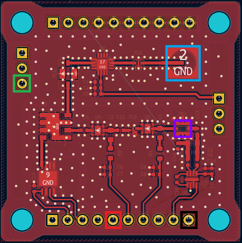
Front-end Gain calibration Procedure
Objective
Measure the total system gain at the output of the RSSI and equalize it.
Steps to follow
-
Turn on equipment
- Spectrum analizer
- Power supply
-
Configure to desired parameters
- Spectrum analizer
- Set center frequency in the middle of VCO output band (6250MHz)
- Set span to match the VCO output band (1400MHz)
- Set RBW and VBW to an adecuate level
- Power supply
- Set Voltage to 3.3V
- Set current limit to 0.3A
- Spectrum analizer
-
Set up nucleo board and PC
- Make sure the proper code is loaded into the nucleo board
-
- Connect the power supply to the payload:
- Vcc to PoL (RED)
- GND to GND (BLACK)
- Connect the DAC output to the DAC_In (GREEN)
- Connect the ADC input to the ADC_Out
- Load the IF Input with a 50 Ohm perfectly matched load.
- Connect the spectrum analizer to the switched measuring pin (PURPLE)
Make connections
- Connect PC to ground (plug in the charger)
- Connect necleo board to computer by USB
- Connect the power supply to the payload:
-
Power on power supply
-
Begin the measurements procedure
- Run the flashed program in Debug mode
- Once the program stops at the breakpoint, collect the calculated mean and plot it in a data processing software like Matlab.
-
Realize the calibration
- Calculate the mean of the collected data and substract it from each frequency bin mean. This will be the deviation.
- Extract the trend line from the deviation.
- Subtract trend line function from the received RSSI value. This will be the calibrated measurement.
-
Reboot the program and check if the equalization is now correct. If it’s not correct repeat the previous step
K-band Noise floor characterization Procedure
Objective
Measure the RSSI obtained though all the 1GHz band with only noise and characterize it.
Steps to follow
-
Turn on equipment
- Spectrum analizer
- Power supply
-
Configure to desired parameters
- Spectrum analizer
- Set center frequency in the middle of RSSI input band (869MHz)
- Set enough span to observe the RSSI input band (30MHz)
- Set RBW and VBW to an adecuate level
- Power supply
- Set Voltage to 3.3V
- Set current limit to 0.3A
- Spectrum analizer
-
Set up nucleo board and PC
- Make sure the proper code is loaded into the nucleo board
-
Make connections
- Connect the power supply to the payload:
- Vcc to PoL (RED)
- GND to GND (BLACK)
- Connect the DAC output to the DAC_In (GREEN)
- Connect the ADC input to the ADC_Out
- Load the IF Input with a 50 Ohm perfectly matched load.
- Connect the spectrum analizer to the switched measuring pin (PURPLE)
- Connect PC to ground (plug in the charger).
- Connect necleo board to computer by USB.
- Connect the power supply to the payload:
-
Power on power supply.
-
Begin the measurements procedure
- Run the flashed program in Debug mode.
- Measure the signal observed with the spectrum analyzer.
- Disconnect the spectrum analizer connected to the switched measuring pin (PURPLE).
- Once the program stops at the breakpoint, collect the calculated mean and plot it in a data processing software like Matlab.
-
Analyze the collected data.
K-band CW characterization Procedure
Objective
Measure the RSSI obtained though all the 1GHz band when inputting a CW and characterize it.
Steps to follow
-
Turn on equipment
- Spectrum analizer
- Signal generator
- Power supply
-
Configure to desired parameters
- Spectrum analizer
- Set center frequency in the middle of RSSI input band (869MHz)
- Set enough span to observe the RSSI input band (30MHz)
- Set RBW and VBW to an adecuate level
- Power supply
- Set Voltage to 3.3V
- Set current limit to 0.3A
- Spectrum analizer
-
Set up nucleo board and PC
- Make sure the proper code is loaded into the nucleo board
-
Make connections
- Connect the power supply to the payload:
- Vcc to PoL (RED)
- GND to GND (BLACK)
- Connect the DAC output to the DAC_In (GREEN)
- Connect the ADC input to the ADC_Out
- Connect the signal generator output to the IF input PIN (BLUE)
- Connect the spectrum analizer to the switched measuring pin (PURPLE)
- Connect PC to ground (plug in the charger).
- Connect necleo board to computer by USB.
- Connect the power supply to the payload:
-
Power on power supply.
-
Begin the measurements procedure
- Run the flashed program in Debug mode.
- Measure the signal observed with the spectrum analyzer.
- Disconnect the spectrum analizer connected to the switched measuring pin (PURPLE).
- Once the program stops at the breakpoint, collect the calculated mean and plot it in a data processing software like Matlab.
-
Analyze the collected data.
P/L3 Envelope Detection characterization Procedure
Objective
Characterize the capacity of the RFI Monitoring system to detect signals by Envelope Detection method.
Steps to follow
-
Turn on equipment
- Power supply
- Signal generator
-
Configure to desired parameters
- Power supply
- Set Voltage to 3.3V
- Set current limit to 0.3A
- Signal generator
- Set output frequency to some IF Band frequency
- Power supply
-
Set up nucleo board and PC
- Make sure the proper code is loaded into the nucleo board
-
Make connections
- Connect the power supply to the payload:
- Vcc to PoL (RED)
- GND to GND (BLACK)
- Connect the DAC output to the DAC_In (GREEN)
- Connect the ADC input to the ADC_Out
- Load the IF Input with a 50 Ohm perfectly matched load.
- Connect PC to ground (plug in the charger).
- Connect necleo board to computer by USB.
- Connect the power supply to the payload:
-
Power on power supply.
-
Begin the measurements procedure
- Run the flashed program in Debug mode.
- Once the program stops at the breakpoint, collect the calculated mean and plot it in a data processing software like Matlab.
-
Analyze the collected data.
P/L3 Statistical pulsed signal characterization Procedure
Objectives
Characterize the capacity of the RFI Monitoring system to detect pulsed signals by statistical algorithms.
Steps to follow
-
Turn on equipment
- Power supply
- Signal generator
-
Configure to desired parameters
- Power supply
- Set Voltage to 3.3V
- Set current limit to 0.3A
- Signal generator
- Set output frequency to some IF Band frequency periodic pulsed signals
- Power supply
-
Set up nucleo board and PC
- Make sure the proper code is loaded into the nucleo board
-
Make connections
- Connect the power supply to the payload:
- Vcc to PoL (RED)
- GND to GND (BLACK)
- Connect the DAC output to the DAC_In (GREEN)
- Connect the ADC input to the ADC_Out
- Load the IF Input with a 50 Ohm perfectly matched load.

- Connect PC to ground (plug in the charger).
- Connect necleo board to computer by USB.
- Connect the power supply to the payload:
-
Power on power supply.
-
Begin the measurements procedure
- Run the flashed program in Debug mode.
- Once the program stops at the breakpoint, collect the calculated mean and plot it in a data processing software like Matlab.
-
Analyze the collected data.
Tests as Run
RFI-5G FE-Top SSV asRun 23/10/2023
Document Scope
The objective of this document is to detail the procedures, results and conclusions to properly test at subsystem level the RFI-5G front-end top board. Several parts will be tested:
- Test of the LNA chain
- Test of the LO chain
- Test of the Front-End top board RF
- Test of the temperature sensor
The as run versions of this document will have the title as "RFI-5G FE-Top SSV as run dd/mm/yyyy".
Test of the LNA chain
Test Description and Objectives
The purpose of this test is to validate that the HMC342 LNA amplifier provides the expected +19 dB of gain for input signals between 24 to 25 GHz, and that the band-pass filter does not introduce more than the expected -4 dB of losses.
Since the probing used is not the frequency range used, this is only a qualitative test to check if the LNA is providing gain and validate that the consumption is nominal.
Requirements Verification
This test does not verify any requirement, and is only to check that the board part works as expected.
Test Set-Up
The required components for this test are the following:
| RFI-5G front-end top board |
|
| C.FL to SMA-2.92mm adapter |
|
| C.FL cable |
|
| RF probe |
|
| SMA 50 Ohm RF load |
|
| DC Block N to SMA adapter |
|
| Power supply |
|
| Signal Generator capable of at least 25 GHz |
|
| Spectrum Analyzer capable of at least 25 GHz |
|
| 2x Jumper cables |
|
| 2x Banana cables |
|
| 2x Crocodrile clips |
|
| 2x SMA 2.92 mm cables |
|
| SMA to SMP cable |
|
The steps to prepare the setup are the following:
- Connect the output from the signal generator to the antenna input of the RFI-5G front-end top board by using the C.FL cable and the C.FL to 2.92 mm adapter.
- Connect the power supply to the Vcc_LNA1 and GND pins with the jumper cables and the crocodile clips.
- Connect the DC-block N to SMA adapter to the spectrum analyzer input.
- Connect the RF probe to the spectrum analyzer using one SMA cable.
- Connect the SMA 50 Ohm RF load to the output of the mixer with the SMA to SMP cable.
The diagram below represents the initial setup:
Pass/Fail Criteria
The test will be considered successful if the LNA shows to provide gain (~19 dB) and the power consumption matches the expected one (~43 mA at 3.3 V). There is though some margin accepted, since the RF probe and cables are not rated for the frequency range used.
Test Plan
|
Step ID |
Description |
Pass/Fail Criteria |
Actual |
Passed [Y/N] |
| RFI-5G-TOP-LNA-000 |
Make sure that the power supply and signal generator outputs are off. | Passes if power supply and signal generator outputs are off. |
ok |
y |
| RFI-5G-TOP-LNA-010 |
Prepare the setup as stated in 2.3. |
Passes if setup prepared. |
setup done |
y |
| RFI-5G-TOP-LNA-020 |
Set the power supply to 3 V and limit the current to 60 mA. |
Passes if power supply set. |
power supply set |
y |
| RFI-5G-TOP-LNA-030 |
Set the signal generator to: f = 24.5 GHz Pout = -70 dBm |
Passes if signal generator set. |
signal generator set |
y |
| RFI-5G-TOP-LNA-040 |
Set the spectrum analyzer to: f = 24.5 GHz Span = 10 MHz RBW = 10 kHz VBW = 1 kHz Trace = Max Hold |
Passes if spectrum analyzer set. |
spectrum analyzer set |
y |
| RFI-5G-TOP-LNA-050 |
Switch on the signal generator output. |
Passes if signal generator output is on. |
signal generator on |
y |
| RFI-5G-TOP-LNA-060 |
Switch on the power supply. If the power supply is limiting switch it off immediately. |
Passes if power supply is on and not current limiting. |
power supply on |
y |
| RFI-5G-TOP-LNA-070 |
Note the voltage and current. If the current consumption is abnormal switch it off immediately. |
Passes if voltage and current are within specification (some margin is allowed but has to be explained why). |
Voltage: 2.99 V Current: 40 mA |
y |
| RFI-5G-TOP-LNA-080 |
With the RF probe, probe the input of the LNA by carefully touching with the signal pogo-pin the RF input pin of the LNA. |
Passes if a signal is shown in the spectrum analyzer. |
signal appears if signal generator power is -50 dBm due to probe |
y |
| RFI-5G-TOP-LNA-090 | Set the trace mode in the spectrum analyzer to VIEW to freeze the image. |
Passes if trace mode is VIEW. |
trace mode VIEW |
y |
|
RFI-5G-TOP-LNA-100 |
Add a second trace in the spectrum analyzer with the same configuration as the first one. |
Passes if spectrum analyzer set. |
spectrum analyzer set |
y |
| RFI-5G-TOP-LNA-110 | With the RF probe, probe the output of the LNA by carefully touching with the signal pogo-pin the RF output pin of the LNA. |
Passes if a signal is shown in the spectrum analyzer. | signal shows in spectrum analyzer |
y |
| RFI-5G-TOP-LNA-120 | Set the trace mode in the spectrum analyzer to VIEW to freeze the image. |
Passes if trace mode is VIEW. |
trace mode VIEW |
y |
| RFI-5G-TOP-LNA-130 |
Add one marker to the peak of trace 1, and another marker that measures the delta in the peak of trace 2. Note the gain and frequency delta values. |
Passes if the gain is within specification (some margin is allowed but has to be explained why). |
Gain: 15.8 dB Frequency: 0 Hz |
y |
| RFI-5G-TOP-LNA-140 |
Capture the screen of the spectrum analyzer and save it into a USB drive. |
Passes if .wmf is saved into a USB drive. |
File name: LNA_001.wmf |
y |
| RFI-5G-TOP-LNA-150 |
Add a third trace in the spectrum analyzer with the same configuration as the first one. |
Passes if spectrum analyzer set. |
third trace added |
y |
| RFI-5G-TOP-LNA-160 | With the RF probe, probe the output of the band-pass filter by carefully touching with the signal pogo-pin the RF output pin of the filter. | Passes if the gain is within specification (some margin is allowed but has to be explained why). |
signal shows in spectrum analyzer |
y |
| RFI-5G-TOP-LNA-170 | Set the trace mode in the spectrum analyzer to VIEW to freeze the image. |
Passes if trace mode is VIEW. |
trace mode VIEW |
y |
| RFI-5G-TOP-LNA-180 |
Add a third marker in trace 3. Note the power and frequency delta values with marker 1. |
Passes if the gain is within specification (some margin is allowed but has to be explained why). |
Gain: 11.15 dB Frequency: 0 Hz |
y |
| RFI-5G-TOP-LNA-190 |
Capture the screen of the spectrum analyzer and save it into a USB drive. |
Passes if .wmf is saved into a USB drive. |
File name: LNA_002.wmf |
y |
| RFI-5G-TOP-LNA-200 |
Switch off the power supply and the signal generator. |
Passes if power supply and signal generator are off. |
power supply and signal generator off |
y |
| RFI-5G-TOP-LNA-210 |
If all steps are passed, proceed with next test. |
Passes if all steps passed. |
Discussion in results |
y |
Test Results
LNA:
Perceived LNA gain is of ~16 dB. Compared to the expected 19.2 dB of gain, the performance is considered valid, since the measuring technique introduces losses that are not accounted for. Additionally, the power consumption of 40 mA seems o be nominal since the expected was 43 mA.

Band-pass filter:
The band-pass filter seems to introduce ~4 dB of losses, which was expected from the specifications.

Anomalies
The signal power from the signal generator has been increased to 50 dBm because of the probing method used, otherwise the signal was not strong enough to be coupled to the probe and appear in the spectrum analyzer measurement.
Conclusions
This test concludes that the LNA chain implementation performs as expected.
Test of the LO chain
Test Description and Objectives
The purpose of this test is to validate that the LO chain works as intended. This means that the HMC506 VCO provides a tone at the expected 8665.5 MHz, and that the HMC342 LO amplifier provides gain (~19 dB) so that the LO input of the mixer is over 12 dBm (~14 dBm).
Since the probing used is not the frequency range used, this is only a qualitative test to check if the LO chain is providing the correct LO tone to the mixer and that the consumption is nominal.
Requirements Verification
This test does not verify any requirement, and is only to check that the board part works as expected.
Test Set-Up
The required components for this test are the following:
| RFI-5G front-end top board |
|
| C.FL to SMA-2.92mm adapter |
|
| C.FL cable |
|
| RF probe |
|
| SMA 50 Ohm RF load |
|
| DC Block N to SMA adapter |
|
| Power supply |
|
| Spectrum Analyzer capable of at least 25 GHz |
|
| 6x Jumper cables |
|
| 6x Banana cables |
|
| 6x Crocodrile clips |
|
| 2x SMA 2.92 mm cables |
|
| SMA to SMP cable |
|
The steps to prepare the setup are the following:
- Connect the output from the signal generator to the antenna input of the RFI-5G front-end top board by using the C.FL cable and the C.FL to 2.92 mm adapter.
- Connect the first channel of the power supply to the Vcc_VCO and GND pins with the jumper cables and the crocodile clips.
- Connect the second channel of the power supply to the Vtune1 and GND pins with the jumper cables and the crocodile clips.
- Connect the third channel of the power supply to the Vcc_IF1Amp and GND pins with the jumper cables and the crocodile clips.
- Connect the DC-block N to SMA adapter to the spectrum analyzer input.
- Connect the RF probe to the spectrum analyzer using one SMA cable.
- Connect the SMA 50 Ohm RF load to the output of the mixer with the SMA to SMP cable.
The diagram below represents the initial setup:
Pass/Fail Criteria
The test will be considered successful if the LO shows a tone at 8665.5 MHz +- 5%, if the LO amplifier provides the expected gain (~19 dB) and if the level of the LO input of the mixer is over 10 dBm. Additionally, the current consumption has to be nominal.
Test Plan
|
Step ID |
Description |
Pass/Fail Criteria |
Actual |
Passed [Y/N] |
| RFI-5G-TOP-LO-000 |
Make sure that the power supply is off. |
Passes if power supply and signal generator outputs are off. |
power supply off |
y |
| RFI-5G-TOP-LO-010 |
Prepare the setup as stated in 3.3. |
Passes if setup prepared. |
setup prepared |
y |
| RFI-5G-TOP-LO-020 |
Set the first channel of the power supply to 3 V and limit the current to 100 mA. |
Passes if power supply set. |
ch1 set |
y |
| RFI-5G-TOP-LO-030 |
Set the second channel of the power supply to 8.7 V and limit the current to 10 mA. |
Passes if power supply set. |
ch2 set |
y |
| RFI-5G-TOP-LO-040 | Set the third channel of the power supply to 3 V and limit the current to 60 mA. |
Passes if power supply set. |
ch3 set |
y |
| RFI-5G-TOP-LO-050 |
Set the spectrum analyzer to: f = 8665.5 MHz Span = 100 MHz RBW = 100 kHz VBW = 3 kHz Trace = Clear/Write |
Passes if spectrum analyzer set. |
spectrum analyzer set |
y |
| RFI-5G-TOP-LO-060 |
Switch on the first channel of the power supply. If the power supply is limiting switch it off immediately. |
Passes if power supply is on and not current limiting. |
ch1 on |
y |
| RFI-5G-TOP-LO-070 |
Switch on the first channel of the power supply. If the power supply is limiting switch it off immediately. |
Passes if power supply is on and not current limiting. |
ch2 on |
y |
| RFI-5G-TOP-LO-080 |
Note the voltage and current. If the current consumption is abnormal switch it off immediately. |
Passes if voltage and current are within specification (some margin is allowed but has to be explained why) |
CH1 Voltage: 3 V Current: 81 mA CH2 Voltage: 8.7 V Current: 0 mA |
y |
| RFI-5G-TOP-LO-080 |
With the RF probe, probe the output of the VCO by carefully touching with the signal pogo-pin the RF output pin of the LNA. |
Passes if a signal is shown in the spectrum analyzer. |
Signal present in spectrum analyzer |
y |
| RFI-5G-TOP-LO-090 | Adjust the Vtune1 voltage until the LO frequency is centered to the desired 8665.5 MHz. |
Passes if LO frequency is ~8665.5 MHz. |
CH2 Voltage: 8.17 V frequency: 8665.5 MHz |
y |
| RFI-5G-TOP-LO-100 | Set the trace mode in the spectrum analyzer to VIEW to freeze the image. |
Passes if trace mode is VIEW. |
trace mode VIEW |
y |
| RFI-5G-TOP-LO-110 | Capture the screen of the spectrum analyzer and save it into a USB drive. |
Passes if .wmf is saved into a USB drive. |
File name: VCO-001.wmf |
y |
| RFI-5G-TOP-LO-120 | Set the trace mode in the spectrum analyzer to CLEAR/WRITE to clear the spectrum. |
Passes if trace mode is CLEAR/WRITE. |
trace mode CLEAR/WRITE |
y |
|
RFI-5G-TOP-LO-130 |
Set the spectrum analyzer to: f = 17331 MHz Span = 200 MHz RBW = 100 kHz VBW = 3 kHz Reference level = 10 dBm Trace = Max Hold |
Passes if spectrum analyzer set. |
spectrum analyzer set |
y |
| RFI-5G-TOP-LO-140 | With the RF probe, probe the output of the frequency multiplier by carefully touching with the signal pogo-pin the RF output pin of the frequency multiplier. |
Passes if a signal is shown in the spectrum analyzer. | signal shows in spectrum analyzer |
y |
| RFI-5G-TOP-LO-150 | Set the trace mode in the spectrum analyzer to VIEW to freeze the image. |
Passes if trace mode is VIEW. |
trace mode VIEW |
y |
| RFI-5G-TOP-LO-160 |
Add one marker at the peak. Note the power and frequency values. | Passes if power and frequency are within specification. |
Power: -25.92 dBm Frequency: 17335.8 MHz |
y |
| RFI-5G-TOP-LO-170 |
Add a second trace in the spectrum analyzer with the same configuration as the first one. | Passes if spectrum analyzer set. | spectrum analyzer set |
y |
| RFI-5G-TOP-LO-180 |
Switch on the third channel of the power supply. If the power supply is limiting switch it off immediately. |
Passes if power supply is on and not current limiting. |
ch3 on |
y |
| RFI-5G-TOP-LO-190 | Note the voltage and current. If the current consumption is abnormal switch it off immediately. |
Passes if voltage and current are within specification (some margin is allowed but has to be explained why) |
CH3 Voltage: 3 V Current: 44 mA |
y |
| RFI-5G-TOP-LO-200 |
With the RF probe, probe the output of the LO amplifier by carefully touching with the signal pogo-pin the RF output pin of the LO amplifier. |
Passes if a signal is shown in the spectrum analyzer. |
signal shows in spectrum analyzer |
y |
| RFI-5G-TOP-LO-210 | Set the trace mode in the spectrum analyzer to VIEW to freeze the image. |
Passes if trace mode is VIEW. |
trace mode VIEW |
y |
| RFI-5G-TOP-LO-220 | Add one marker to the peak of trace 1, and another marker that measures the delta in the peak of trace 2. Note the power and frequency delta values. |
Passes if the gain is within specification (some margin is allowed but has to be explained why). |
Power: 11.07 dB Frequency: 0.8 kHz |
y |
| RFI-5G-TOP-LO-230 | Capture the screen of the spectrum analyzer and save it into a USB drive. |
Passes if .wmf is saved into a USB drive. |
File name: DOUBLER_001.wmf |
y |
| RFI-5G-TOP-LO-240 | Switch off the power supply and the signal generator. |
Passes if power supply and signal generator are off. |
power supply off |
y |
| RFI-5G-TOP-LO-250 | If all steps are passed, proceed with next test. |
Passes if all steps passed. |
Discussion in results |
y |
Test Results
VCO:
The VCO output provides a tone centered to a frequency provided by the Vtune voltage. In order to obtain the desired 8665.5 MHz of VCO frequency, the tuning voltage has been lowered from the expected 8.7 V to 8.17 V. Additionally, the frequency tuning appears to be erroneous: when the front-end is shifted or the cables are moved, the output of the VCO varies significantly.
The power consumption of the VCO is of 81 mA at 3 V, which is higher than the expected 77 mA from the specification. The reasoning of this increase in consumption might be the bad connections used with the jumper.

Frequency doubler and amplifier:
The frequency doubler doubles the VCO output tone accordingly. The losses introduced by the doubling cannot be measured accurately.
The LO amplifier provides a net gain of ~11 dB, and when considering the 50 Ohm resistor in series at its input to reduce the signal power that adds ~4dB of extra losses , the behavior of the amplifier is in pair with the LNA (is the same ic). The power consumption appears to be of a nominal 40 mA.

Anomalies
The list of anomalies is shown below:
- Erroneous VCO frequency tuning when front-end or cables are shifted.
- Higher power consumption than nominal of the VCO.
- The LO signal at the input of the mixer seems to be of not powerful enough to drive the mixer.
Conclusions
The VCO behavior is validated, but its characteristics need to be measured with the interface board attached, to reduce the impedance of the jumper cables used and improve the performance.
Test of the Front-end Top board RF
Test Description and Objectives
The purpose of this test is to validate the correct functioning of the RF part of the RFI-5G front-end top, i.e., with an input signal between 24-25 GHz, the signal is down-converted to an intermediate signal with frequency between 6669-76669 MHz, with a net gain of 5 dB.
Requirements Verification
This test does not verify any requirement, and is only to check that the board part works as expected.
Test Set-Up
The required components for this test are the following:
| RFI-5G front-end top board |
|
| RFI-5G interface board with inverse connectors |
|
| C.FL to SMA-2.92mm adapter |
|
| C.FL cable |
|
| DC Block N to SMA adapter |
|
| Power supply |
|
| Signal Generator capable of at least 25 GHz |
|
| Spectrum Analyzer capable of at least 25 GHz |
|
| 2x Banana cables |
|
| SMA 2.92 mm cables |
|
| SMA to SMP cable |
|
The steps to prepare the setup are the following:
- Mate the RFI-5G front-end top board with the RFI-5G interface board that has the inverse pin header.
- Connect the EGSE to the power supply with the banana cables.
- Connect the output from the signal generator to the antenna input of the RFI-5G front-end top board by using the C.FL cable and the C.FL to 2.92 mm adapter.
- Connect the DC-block N to SMA adapter to the spectrum analyzer input.
- Connect the RFI-5G front-end top board output to the spectrum analyzer using the SMA to SMP cable.
The diagram below represents the initial setup:
Pass/Fail Criteria
The test will be considered successful if the output of the RFI-5G front-end top board is a signal between 6669-7669 MHz when the antenna input is between 24-25 GHz, and the board provides a net gain of +5 dB. Additionally, the current consumption has to be nominal.
Test Plan
|
Step ID |
Description |
Pass/Fail Criteria |
Actual |
Passed [Y/N] |
| RFI-5G-TOP-RF-000 |
Make sure that the power supply and signal generator outputs are off. | Passes if power supply and signal generator outputs are off. |
power supply and signal generator off |
y |
| RFI-5G-TOP-RF-010 |
Prepare the setup as stated in 4.3. |
Passes if setup prepared. |
setup prepared |
y |
| RFI-5G-TOP-RF-020 |
Set the first channel of the power supply to 3.3 V and limit the current to 200 mA. |
Passes if power supply set. |
power supply set |
y |
| RFI-5G-TOP-RF-030 |
Set the spectrum analyzer to: f = 7169 MHz Span = 200 MHz RBW = 100 kHz VBW = 3 kHz Reference level = -20 dBm Trace = Clear/Write |
Passes if spectrum analyzer set. |
spectrum analyzer set |
y |
| RFI-5G-TOP-RF-040 |
Set the signal generator to: f = 24.5 GHz Pout = -80 dBm |
Passes if signal generator set. | signal generator set |
y |
| RFI-5G-TOP-RF-050 |
Switch on the first channel of the power supply. If the power supply is limiting switch it off immediately. |
Passes if power supply is on and not current limiting. |
power supply on |
y |
| RFI-5G-TOP-RF-060 | Note the voltage and current. If the current consumption is abnormal switch it off immediately. |
Passes if voltage and current are within specification (some margin is allowed but has to be explained why). |
CH1 Voltage: 3.3 V Current: 150 mA |
y |
| RFI-5G-TOP-RF-070 | Enable the output of the signal generator. | Passes if signal generator output is enabled. | signal generator enabled |
y |
| RFI-5G-TOP-RF-080 | Note the voltage and current. If the current consumption is abnormal switch it off immediately. |
Passes if voltage and current are same as in RFI-5G-TOP-RF-060. |
CH1 Voltage: 3.3 V Current: 150 mA |
n |
| RFI-5G-TOP-RF-090 | Add one marker at the peak. Note the frequency and power of the intermediate signal. Additionally compute the net gain and the frequency shift. | Passes if the net gain is +5 dB and the frequency shift of 17331 MHz. |
frequency = Power = frequency shift = Gain = |
n |
| RFI-5G-TOP-RF-100 | Set the trace mode in the spectrum analyzer to VIEW to freeze the image. |
Passes if trace mode is VIEW. |
||
| RFI-5G-TOP-RF-110 | Capture the screen of the spectrum analyzer and save it into a USB drive. |
Passes if .wmf is saved into a USB drive. |
File name: |
|
| RFI-5G-TOP-RF-120 | Set the trace mode in the spectrum analyzer to CLEAR/WRITE to clear the spectrum. |
Passes if trace mode is CLEAR/WRITE. | ||
| RFI-5G-TOP-RF-130 |
Switch off the output of the signal generator. |
Passes if signal generator output is off. |
||
| RFI-5G-TOP-RF-140 |
Set the spectrum analyzer to: f = 7169 MHz Span = 1200 MHz RBW = 300 kHz VBW = 30 kHz Trace = Max Hold |
Passes if spectrum analyzer set. |
||
| RFI-5G-TOP-RF-150 |
Set the signal generator to: Mode = frequency sweep f = 24.5 GHz Span = 1 GHz Step = 10 MHz P = -80 dBm |
Passes if signal generator set. |
|
|
| RFI-5G-TOP-RF-160 |
Switch on the output of the signal generator. |
Passes if signal generator output is on. |
||
| RFI-5G-TOP-RF-170 | Wait until a complete frequency sweep is done. | Passes when complete frequency sweep finishes. | ||
| RFI-5G-TOP-RF-180 | Check qualitatively the flatness of the RFI-5G front-end top board RF output. | Passes if the RF output is "flat". | ||
| RFI-5G-TOP-RF-190 | Set the trace mode in the spectrum analyzer to VIEW to freeze the image. |
Passes if trace mode is VIEW. |
|
|
| RFI-5G-TOP-RF-200 | Capture the screen of the spectrum analyzer and save it into a USB drive. |
Passes if .wmf is saved into a USB drive. |
File name: |
|
| RFI-5G-TOP-RF-210 | Switch off the power supply and the signal generator. |
Passes if power supply and signal generator are off. |
||
| RFI-5G-TOP-RF-220 | If all steps are passed, proceed with next test. |
Passes if all steps passed. |
Test Results
The mixer does not seem to perform the frequency downconversion
Upon investigation
Anomalies
List of deviations to the Test Specification and Procedure and non-conformances witnessed during the test campaign, including a brief description, the close-out status and reference to the relevant reports.
Conclusions
The Conclusions shall include (where needed as annex):
- Test results, including as a minimum:
- Requirement to be verified
- Subsections of test campaign in which that requirement was verified (e.g. Thermal Vacuum RFT 1, Inspection 1, Inspection 2, ...)
- Close-out judgement (compliance status) and rationale, per subsection of the test
- Traceability to used documentation
- Conformance or deviation including references
- Overall conclusion on the success of the test, including clearly stated and described open issues and possible remediating actions.
- Test Readiness Review minutes and Post Test Review minutes
Test of the temperature sensor
Test Description and Objectives
The purpose of this test is to validate the correct functioning of temperature sensor in the RFI-5G front-end top board, and that the sensor library code functions correctly.
Requirements Verification
This test does not verify any requirement, and is only to check that the board part works as expected.
Test Set-Up
The required components for this test are the following:
| RFI-5G front-end top board |
|
| RFI-5G interface board with inverse connectors |
|
| RFI-5G EGSE |
|
| STM32 Nucleo-L476RG board |
|
| USB A-to-mini cable |
|
| Power supply |
|
| 2x Banana cables |
|
| 2x Jumper cables |
|
| Temperature sensor test code |
NA |
The steps to prepare the setup are the following:
- Mate the RFI-5G front-end top board with the RFI-5G interface board that has the inverse pin header.
- Connect the EGSE to the power supply with the banana cables.
- Connect the output from the signal generator to the antenna input of the RFI-5G front-end top board by using the C.FL cable and the C.FL to 2.92 mm adapter.
- Connect the DC-block N to SMA adapter to the spectrum analyzer input.
- Connect the RFI-5G front-end top board output to the spectrum analyzer using the SMA to SMP cable.
The diagram below represents the initial setup:
Missing setup picture
Pass/Fail Criteria
Description of which metric is used to perform the test and when it is considered that the test passed or not. If different metrics are used, it is important to define when the test passed or not (e.g. when all the metrics are in the pass criteria, or when only one of them).
Test Plan
This section includes the test sequence necesary to do the test. The test sequence must include all the steps, from the set-up up to the conclusion of the test.
Test Results
Description of the Test results with supporting data.
- Test name, test execution dates, the test facility used and the operators
- Test Logbooks
- “As-run” procedures (to be provided in annex)
- Test facility results (if applicable)
- Photographs relevant to the set-up(s) and inspection(s) (may also be added in the Conclusions to clarify a close-out judgement, e.g. for an inspection)
- Analysis of the test data and relevant assessment.
- Synthesis of the overall test results per verification (e.g. Vibration, Inspection 1, Inspection 2, etc.).
Anomalies
List of deviations to the Test Specification and Procedure and non-conformances witnessed during the test campaign, including a brief description, the close-out status and reference to the relevant reports.
Conclusions
The Conclusions shall include (where needed as annex):
- Test results, including as a minimum:
- Requirement to be verified
- Subsections of test campaign in which that requirement was verified (e.g. Thermal Vacuum RFT 1, Inspection 1, Inspection 2, ...)
- Close-out judgement (compliance status) and rationale, per subsection of the test
- Traceability to used documentation
- Conformance or deviation including references
- Overall conclusion on the success of the test, including clearly stated and described open issues and possible remediating actions.
- Test Readiness Review minutes and Post Test Review minutes
RFI-5G FE-Top SSV as run 13/11/2023 (1)
Document Scope
The objective of this document is to detail the procedures, results and conclusions to properly test at subsystem level the RFI-5G front-end top board. Several parts will be tested:
- Test of the LNA chain
- Test of the LO chain
- Test of the Front-End top board RF
- Test of the temperature sensor
The as run versions of this document will have the title as "RFI-5G FE-Top SSV as run dd/mm/yyyy".
Test of the LNA chain
Test Description and Objectives
The purpose of this test is to validate that the HMC342 LNA amplifier provides the expected +19 dB of gain for input signals between 24 to 25 GHz, and that the band-pass filter does not introduce more than the expected -4 dB of losses.
Since the probing used is not the frequency range used, this is only a qualitative test to check if the LNA is providing gain and validate that the consumption is nominal.
Requirements Verification
This test does not verify any requirement, and is only to check that the board part works as expected.
Test Set-Up
The required components for this test are the following:
| RFI-5G front-end top board |
|
| C.FL to SMA-2.92mm adapter |
|
| C.FL cable |
|
| RF probe |
|
| SMA 50 Ohm RF load |
|
| DC Block N to SMA adapter |
|
| Power supply |
|
| Signal Generator capable of at least 25 GHz |
|
| Spectrum Analyzer capable of at least 25 GHz |
|
| 2x Jumper cables |
|
| 2x Banana cables |
|
| 2x Crocodrile clips |
|
| 2x SMA 2.92 mm cables |
|
| SMA to SMP cable |
|
The steps to prepare the setup are the following:
- Connect the output from the signal generator to the antenna input of the RFI-5G front-end top board by using the C.FL cable and the C.FL to 2.92 mm adapter.
- Connect the power supply to the Vcc_LNA1 and GND pins with the jumper cables and the crocodile clips.
- Connect the DC-block N to SMA adapter to the spectrum analyzer input.
- Connect the RF probe to the spectrum analyzer using one SMA cable.
- Connect the SMA 50 Ohm RF load to the output of the mixer with the SMA to SMP cable.
The diagram below represents the initial setup:
Pass/Fail Criteria
The test will be considered successful if the LNA shows to provide gain (~19 dB) and the power consumption matches the expected one (~43 mA at 3.3 V). There is though some margin accepted, since the RF probe and cables are not rated for the frequency range used.
Test Plan
|
Step ID |
Description |
Pass/Fail Criteria |
Actual |
Passed [Y/N] |
| RFI-5G-TOP-LNA-000 |
Make sure that the power supply and signal generator outputs are off. | Passes if power supply and signal generator outputs are off. |
y | |
| RFI-5G-TOP-LNA-010 |
Prepare the setup as stated in 2.3. |
Passes if setup prepared. |
y | |
| RFI-5G-TOP-LNA-020 |
Set the power supply to 3 V and limit the current to 60 mA. |
Passes if power supply set. |
y | |
| RFI-5G-TOP-LNA-030 |
Set the signal generator to: f = 24.5 GHz Pout = -70 dBm |
Passes if signal generator set. |
y | |
| RFI-5G-TOP-LNA-040 |
Set the spectrum analyzer to: f = 24.5 GHz Span = 10 MHz RBW = 10 kHz VBW = 1 kHz Trace = Max Hold |
Passes if spectrum analyzer set. |
y | |
| RFI-5G-TOP-LNA-050 |
Switch on the signal generator output. |
Passes if signal generator output is on. |
y | |
| RFI-5G-TOP-LNA-060 |
Switch on the power supply. If the power supply is limiting switch it off immediately. |
Passes if power supply is on and not current limiting. |
y | |
| RFI-5G-TOP-LNA-070 |
Note the voltage and current. If the current consumption is abnormal switch it off immediately. |
Passes if voltage and current are within specification (some margin is allowed but has to be explained why). |
Voltage:3V Current:42 mA |
y |
| RFI-5G-TOP-LNA-080 |
With the RF probe, probe the input of the LNA by carefully touching with the signal pogo-pin the RF input pin of the LNA. |
Passes if a signal is shown in the spectrum analyzer. |
max hold of -70.61 dBm at center frequency |
y |
| RFI-5G-TOP-LNA-090 | Set the trace mode in the spectrum analyzer to VIEW to freeze the image. |
Passes if trace mode is VIEW. |
y | |
|
RFI-5G-TOP-LNA-100 |
Add a second trace in the spectrum analyzer with the same configuration as the first one. |
Passes if spectrum analyzer set. |
y | |
| RFI-5G-TOP-LNA-110 | With the RF probe, probe the output of the LNA by carefully touching with the signal pogo-pin the RF output pin of the LNA. |
Passes if a signal is shown in the spectrum analyzer. | max hold of -46.95 dBm at center frequency | y |
| RFI-5G-TOP-LNA-120 | Set the trace mode in the spectrum analyzer to VIEW to freeze the image. |
Passes if trace mode is VIEW. |
y | |
| RFI-5G-TOP-LNA-130 |
Add one marker to the peak of trace 1, and another marker that measures the delta in the peak of trace 2. Note the gain and frequency delta values. |
Passes if the gain is within specification (some margin is allowed but has to be explained why). |
Gain: 23.66 dB Frequency: 0 Hz Gain between 16 and 26 dB. For 24.5 GHz, the gain should be lower according to datasheet |
n |
| RFI-5G-TOP-LNA-140 |
Capture the screen of the spectrum analyzer and save it into a USB drive. |
Passes if .wmf is saved into a USB drive. |
File name: "LNA1-1 131123.WMF" |
y |
| RFI-5G-TOP-LNA-150 |
Add a third trace in the spectrum analyzer with the same configuration as the first one. |
Passes if spectrum analyzer set. |
y | |
| RFI-5G-TOP-LNA-160 | With the RF probe, probe the output of the band-pass filter by carefully touching with the signal pogo-pin the RF output pin of the filter. | Passes if the gain is within specification (some margin is allowed but has to be explained why). | output level of -54.85 dBm, attenuation of 7.9 dB, much higher than the expected 2 dB of datasheet | n |
| RFI-5G-TOP-LNA-170 | Set the trace mode in the spectrum analyzer to VIEW to freeze the image. |
Passes if trace mode is VIEW. |
y | |
| RFI-5G-TOP-LNA-180 |
Add a third marker in trace 3. Note the power and frequency delta values with marker 1. |
Passes if the gain is within specification (some margin is allowed but has to be explained why). |
Gain: 15.76 dB Frequency: 0 Hz |
n |
| RFI-5G-TOP-LNA-190 |
Capture the screen of the spectrum analyzer and save it into a USB drive. |
Passes if .wmf is saved into a USB drive. |
File name: "LNA1-2 131123.WMF" |
y |
| RFI-5G-TOP-LNA-200 |
Switch off the power supply and the signal generator. |
Passes if power supply and signal generator are off. |
.y | |
| RFI-5G-TOP-LNA-210 |
If all steps are passed, proceed with next test. |
Passes if all steps passed. |
n |
Test Results
Description of the Test results with supporting data.
- Test name, test execution dates, the test facility used and the operators
- Test Logbooks
- “As-run” procedures (to be provided in annex)
- Test facility results (if applicable)
- Photographs relevant to the set-up(s) and inspection(s) (may also be added in the Conclusions to clarify a close-out judgement, e.g. for an inspection)
- Analysis of the test data and relevant assessment.
- Synthesis of the overall test results per verification (e.g. Vibration, Inspection 1, Inspection 2, etc.).
Anomalies
LNA gain much higher than expected, filter attaenuation much higher than expected.
List of deviations to the Test Specification and Procedure and non-conformances witnessed during the test campaign, including a brief description, the close-out status and reference to the relevant reports.
Conclusions
Measurements differ too much from expected values, test is being re-done.
The Conclusions shall include (where needed as annex):
- Test results, including as a minimum:
- Requirement to be verified
- Subsections of test campaign in which that requirement was verified (e.g. Thermal Vacuum RFT 1, Inspection 1, Inspection 2, ...)
- Close-out judgement (compliance status) and rationale, per subsection of the test
- Traceability to used documentation
- Conformance or deviation including references
- Overall conclusion on the success of the test, including clearly stated and described open issues and possible remediating actions.
- Test Readiness Review minutes and Post Test Review minutes
Test of the LO chain
Test Description and Objectives
The purpose of this test is to validate that the LO chain works as intended. This means that the HMC506 VCO provides a tone at the expected 8665.5 MHz, and that the HMC342 LO amplifier provides gain (~19 dB) so that the LO input of the mixer is over 12 dBm (~14 dBm).
Since the probing used is not the frequency range used, this is only a qualitative test to check if the LO chain is providing the correct LO tone to the mixer and that the consumption is nominal.
Requirements Verification
This test does not verify any requirement, and is only to check that the board part works as expected.
Test Set-Up
The required components for this test are the following:
| RFI-5G front-end top board |
|
| C.FL to SMA-2.92mm adapter |
|
| C.FL cable |
|
| RF probe |
|
| SMA 50 Ohm RF load |
|
| DC Block N to SMA adapter |
|
| Power supply |
|
| Spectrum Analyzer capable of at least 25 GHz |
|
| 6x Jumper cables |
|
| 6x Banana cables |
|
| 6x Crocodrile clips |
|
| 2x SMA 2.92 mm cables |
|
| SMA to SMP cable |
|
The steps to prepare the setup are the following:
- Connect the output from the signal generator to the antenna input of the RFI-5G front-end top board by using the C.FL cable and the C.FL to 2.92 mm adapter.
- Connect the first channel of the power supply to the Vcc_VCO and GND pins with the jumper cables and the crocodile clips.
- Connect the second channel of the power supply to the Vtune1 and GND pins with the jumper cables and the crocodile clips.
- Connect the third channel of the power supply to the Vcc_IF1Amp and GND pins with the jumper cables and the crocodile clips.
- Connect the DC-block N to SMA adapter to the spectrum analyzer input.
- Connect the RF probe to the spectrum analyzer using one SMA cable.
- Connect the SMA 50 Ohm RF load to the output of the mixer with the SMA to SMP cable.
The diagram below represents the initial setup:
Pass/Fail Criteria
The test will be considered successful if the LO shows a tone at 8665.5 MHz +- 5%, if the LO amplifier provides the expected gain (~19 dB) and if the level of the LO input of the mixer is over 10 dBm. Additionally, the current consumption has to be nominal.
Test Plan
|
Step ID |
Description |
Pass/Fail Criteria |
Actual |
Passed [Y/N] |
| RFI-5G-TOP-LO-000 |
Make sure that the power supply is off. |
Passes if power supply and signal generator outputs are off. |
||
| RFI-5G-TOP-LO-010 |
Prepare the setup as stated in 3.3. |
Passes if setup prepared. |
||
| RFI-5G-TOP-LO-020 |
Set the first channel of the power supply to 3 V and limit the current to 100 mA. |
Passes if power supply set. |
||
| RFI-5G-TOP-LO-030 |
Set the second channel of the power supply to 8.7 V and limit the current to 10 mA. |
Passes if power supply set. |
||
| RFI-5G-TOP-LO-040 | Set the third channel of the power supply to 3 V and limit the current to 60 mA. |
Passes if power supply set. |
||
| RFI-5G-TOP-LO-050 |
Set the spectrum analyzer to: f = 8665.5 MHz Span = 100 MHz RBW = 100 kHz VBW = 3 kHz Trace = Clear/Write |
Passes if spectrum analyzer set. |
||
| RFI-5G-TOP-LO-060 |
Switch on the first channel of the power supply. If the power supply is limiting switch it off immediately. |
Passes if power supply is on and not current limiting. |
||
| RFI-5G-TOP-LO-070 |
Switch on the first channel of the power supply. If the power supply is limiting switch it off immediately. |
Passes if power supply is on and not current limiting. |
||
| RFI-5G-TOP-LO-080 |
Note the voltage and current. If the current consumption is abnormal switch it off immediately. |
Passes if voltage and current are within specification (some margin is allowed but has to be explained why) |
CH1 Voltage: Current: CH2 Voltage: Current: |
|
| RFI-5G-TOP-LO-080 |
With the RF probe, probe the output of the VCO by carefully touching with the signal pogo-pin the RF output pin of the LNA. |
Passes if a signal is shown in the spectrum analyzer. |
||
| RFI-5G-TOP-LO-090 | Adjust the Vtune1 voltage until the LO frequency is centered to the desired 8665.5 MHz. |
Passes if LO frequency is ~8665.5 MHz. |
CH2 Voltage: frequency: |
|
| RFI-5G-TOP-LO-100 | Set the trace mode in the spectrum analyzer to VIEW to freeze the image. |
Passes if trace mode is VIEW. |
||
| RFI-5G-TOP-LO-110 | Capture the screen of the spectrum analyzer and save it into a USB drive. |
Passes if .wmf is saved into a USB drive. |
File name: |
|
| RFI-5G-TOP-LO-120 | Set the trace mode in the spectrum analyzer to CLEAR/WRITE to clear the spectrum. |
Passes if trace mode is CLEAR/WRITE. | ||
|
RFI-5G-TOP-LO-130 |
Set the spectrum analyzer to: f = 17331 MHz Span = 200 MHz RBW = 100 kHz VBW = 3 kHz Reference level = 10 dBm Trace = Max Hold |
Passes if spectrum analyzer set. |
||
| RFI-5G-TOP-LO-140 | With the RF probe, probe the output of the frequency multiplier by carefully touching with the signal pogo-pin the RF output pin of the frequency multiplier. |
Passes if a signal is shown in the spectrum analyzer. | ||
| RFI-5G-TOP-LO-150 | Set the trace mode in the spectrum analyzer to VIEW to freeze the image. |
Passes if trace mode is VIEW. |
||
| RFI-5G-TOP-LO-160 |
Add one marker at the peak. Note the power and frequency values. | Passes if power and frequency are within specification. |
Power: Frequency: |
|
| RFI-5G-TOP-LO-170 |
Add a second trace in the spectrum analyzer with the same configuration as the first one. | Passes if spectrum analyzer set. | ||
| RFI-5G-TOP-LO-180 |
Switch on the third channel of the power supply. If the power supply is limiting switch it off immediately. |
Passes if power supply is on and not current limiting. |
||
| RFI-5G-TOP-LO-190 | Note the voltage and current. If the current consumption is abnormal switch it off immediately. |
Passes if voltage and current are within specification (some margin is allowed but has to be explained why) |
CH3 Voltage: Current: |
|
| RFI-5G-TOP-LO-200 |
With the RF probe, probe the output of the LO amplifier by carefully touching with the signal pogo-pin the RF output pin of the LO amplifier. |
Passes if a signal is shown in the spectrum analyzer. | ||
| RFI-5G-TOP-LO-210 | Set the trace mode in the spectrum analyzer to VIEW to freeze the image. |
Passes if trace mode is VIEW. |
||
| RFI-5G-TOP-LO-220 | Add one marker to the peak of trace 1, and another marker that measures the delta in the peak of trace 2. Note the power and frequency delta values. |
Passes if the gain is within specification (some margin is allowed but has to be explained why). |
Power: Frequency: |
|
| RFI-5G-TOP-LO-230 | Capture the screen of the spectrum analyzer and save it into a USB drive. |
Passes if .wmf is saved into a USB drive. |
File name: |
|
| RFI-5G-TOP-LO-240 | Switch off the power supply and the signal generator. |
Passes if power supply and signal generator are off. |
||
| RFI-5G-TOP-LO-250 | If all steps are passed, proceed with next test. |
Passes if all steps passed. |
Test Results
Description of the Test results with supporting data.
- Test name, test execution dates, the test facility used and the operators
- Test Logbooks
- “As-run” procedures (to be provided in annex)
- Test facility results (if applicable)
- Photographs relevant to the set-up(s) and inspection(s) (may also be added in the Conclusions to clarify a close-out judgement, e.g. for an inspection)
- Analysis of the test data and relevant assessment.
- Synthesis of the overall test results per verification (e.g. Vibration, Inspection 1, Inspection 2, etc.).
Anomalies
List of deviations to the Test Specification and Procedure and non-conformances witnessed during the test campaign, including a brief description, the close-out status and reference to the relevant reports.
Conclusions
The Conclusions shall include (where needed as annex):
- Test results, including as a minimum:
- Requirement to be verified
- Subsections of test campaign in which that requirement was verified (e.g. Thermal Vacuum RFT 1, Inspection 1, Inspection 2, ...)
- Close-out judgement (compliance status) and rationale, per subsection of the test
- Traceability to used documentation
- Conformance or deviation including references
- Overall conclusion on the success of the test, including clearly stated and described open issues and possible remediating actions.
- Test Readiness Review minutes and Post Test Review minutes
Test of the Front-end Top board RF
Test Description and Objectives
The purpose of this test is to validate the correct functioning of the RF part of the RFI-5G front-end top, i.e., with an input signal between 24-25 GHz, the signal is down-converted to an intermediate signal with frequency between 6669-76669 MHz, with a net gain of 5 dB.
Requirements Verification
This test does not verify any requirement, and is only to check that the board part works as expected.
Test Set-Up
The required components for this test are the following:
| RFI-5G front-end top board |
|
| RFI-5G interface board with inverse connectors |
|
| C.FL to SMA-2.92mm adapter |
|
| C.FL cable |
|
| DC Block N to SMA adapter |
|
| Power supply |
|
| Signal Generator capable of at least 25 GHz |
|
| Spectrum Analyzer capable of at least 25 GHz |
|
| 2x Banana cables |
|
| SMA 2.92 mm cables |
|
| SMA to SMP cable |
|
The steps to prepare the setup are the following:
- Mate the RFI-5G front-end top board with the RFI-5G interface board that has the inverse pin header.
- Connect the EGSE to the power supply with the banana cables.
- Connect the output from the signal generator to the antenna input of the RFI-5G front-end top board by using the C.FL cable and the C.FL to 2.92 mm adapter.
- Connect the DC-block N to SMA adapter to the spectrum analyzer input.
- Connect the RFI-5G front-end top board output to the spectrum analyzer using the SMA to SMP cable.
The diagram below represents the initial setup:
Pass/Fail Criteria
The test will be considered successful if the output of the RFI-5G front-end top board is a signal between 6669-7669 MHz when the antenna input is between 24-25 GHz, and the board provides a net gain of +5 dB. Additionally, the current consumption has to be nominal.
Test Plan
|
Step ID |
Description |
Pass/Fail Criteria |
Actual |
Passed [Y/N] |
| RFI-5G-TOP-RF-000 |
Make sure that the power supply and signal generator outputs are off. | Passes if power supply and signal generator outputs are off. |
||
| RFI-5G-TOP-RF-010 |
Prepare the setup as stated in 4.3. |
Passes if setup prepared. |
||
| RFI-5G-TOP-RF-020 |
Set the first channel of the power supply to 3.3 V and limit the current to 200 mA. |
Passes if power supply set. |
||
| RFI-5G-TOP-RF-030 |
Set the spectrum analyzer to: f = 7169 MHz Span = 200 MHz RBW = 100 kHz VBW = 3 kHz Reference level = -20 dBm Trace = Clear/Write |
Passes if spectrum analyzer set. |
||
| RFI-5G-TOP-RF-040 |
Set the signal generator to: f = 24.5 GHz Pout = -80 dBm |
Passes if signal generator set. | ||
| RFI-5G-TOP-RF-050 |
Switch on the first channel of the power supply. If the power supply is limiting switch it off immediately. |
Passes if power supply is on and not current limiting. |
||
| RFI-5G-TOP-RF-060 | Note the voltage and current. If the current consumption is abnormal switch it off immediately. |
Passes if voltage and current are within specification (some margin is allowed but has to be explained why). |
Voltage: Current: |
|
| RFI-5G-TOP-RF-070 | Enable the output of the signal generator. | Passes if signal generator output is enabled. | ||
| RFI-5G-TOP-RF-080 | Note the voltage and current. If the current consumption is abnormal switch it off immediately. |
Passes if voltage and current are same as in RFI-5G-TOP-RF-060. |
Voltage: Current: |
|
| RFI-5G-TOP-RF-090 | Add one marker at the peak. Note the frequency and power of the intermediate signal. Additionally compute the net gain and the frequency shift. | Passes if the net gain is +5 dB and the frequency shift of 17331 MHz. |
frequency = Power = frequency shift = Gain = |
|
| RFI-5G-TOP-RF-100 | Set the trace mode in the spectrum analyzer to VIEW to freeze the image. |
Passes if trace mode is VIEW. |
||
| RFI-5G-TOP-RF-110 | Capture the screen of the spectrum analyzer and save it into a USB drive. |
Passes if .wmf is saved into a USB drive. |
File name: |
|
| RFI-5G-TOP-RF-120 | Set the trace mode in the spectrum analyzer to CLEAR/WRITE to clear the spectrum. |
Passes if trace mode is CLEAR/WRITE. | ||
| RFI-5G-TOP-RF-130 |
Switch off the output of the signal generator. |
Passes if signal generator output is off. |
||
| RFI-5G-TOP-RF-140 |
Set the spectrum analyzer to: f = 7169 MHz Span = 1200 MHz RBW = 300 kHz VBW = 30 kHz Trace = Max Hold |
Passes if spectrum analyzer set. |
||
| RFI-5G-TOP-RF-150 |
Set the signal generator to: Mode = frequency sweep f = 24.5 GHz Span = 1 GHz Step = 10 MHz P = -80 dBm |
Passes if signal generator set. |
|
|
| RFI-5G-TOP-RF-160 |
Switch on the output of the signal generator. |
Passes if signal generator output is on. |
||
| RFI-5G-TOP-RF-170 | Wait until a complete frequency sweep is done. | Passes when complete frequency sweep finishes. | ||
| RFI-5G-TOP-RF-180 | Check qualitatively the flatness of the RFI-5G front-end top board RF output. | Passes if the RF output is "flat". | ||
| RFI-5G-TOP-RF-190 | Set the trace mode in the spectrum analyzer to VIEW to freeze the image. |
Passes if trace mode is VIEW. |
|
|
| RFI-5G-TOP-RF-200 | Capture the screen of the spectrum analyzer and save it into a USB drive. |
Passes if .wmf is saved into a USB drive. |
File name: |
|
| RFI-5G-TOP-RF-210 | Switch off the power supply and the signal generator. |
Passes if power supply and signal generator are off. |
||
| RFI-5G-TOP-RF-220 | If all steps are passed, proceed with next test. |
Passes if all steps passed. |
Test Results
Description of the Test results with supporting data.
- Test name, test execution dates, the test facility used and the operators
- Test Logbooks
- “As-run” procedures (to be provided in annex)
- Test facility results (if applicable)
- Photographs relevant to the set-up(s) and inspection(s) (may also be added in the Conclusions to clarify a close-out judgement, e.g. for an inspection)
- Analysis of the test data and relevant assessment.
- Synthesis of the overall test results per verification (e.g. Vibration, Inspection 1, Inspection 2, etc.).
Anomalies
List of deviations to the Test Specification and Procedure and non-conformances witnessed during the test campaign, including a brief description, the close-out status and reference to the relevant reports.
Conclusions
The Conclusions shall include (where needed as annex):
- Test results, including as a minimum:
- Requirement to be verified
- Subsections of test campaign in which that requirement was verified (e.g. Thermal Vacuum RFT 1, Inspection 1, Inspection 2, ...)
- Close-out judgement (compliance status) and rationale, per subsection of the test
- Traceability to used documentation
- Conformance or deviation including references
- Overall conclusion on the success of the test, including clearly stated and described open issues and possible remediating actions.
- Test Readiness Review minutes and Post Test Review minutes
Test of the temperature sensor
Test Description and Objectives
The purpose of this test is to validate the correct functioning of temperature sensor in the RFI-5G front-end top board, and that the sensor library code functions correctly.
Requirements Verification
This test does not verify any requirement, and is only to check that the board part works as expected.
Test Set-Up
The required components for this test are the following:
| RFI-5G front-end top board |
|
| RFI-5G interface board with inverse connectors |
|
| RFI-5G EGSE |
|
| STM32 Nucleo-L476RG board |
|
| USB A-to-mini cable |
|
| Power supply |
|
| 2x Banana cables |
|
| 2x Jumper cables |
|
| Temperature sensor test code |
NA |
The steps to prepare the setup are the following:
- Mate the RFI-5G front-end top board with the RFI-5G interface board that has the inverse pin header.
- Connect the EGSE to the power supply with the banana cables.
- Connect the output from the signal generator to the antenna input of the RFI-5G front-end top board by using the C.FL cable and the C.FL to 2.92 mm adapter.
- Connect the DC-block N to SMA adapter to the spectrum analyzer input.
- Connect the RFI-5G front-end top board output to the spectrum analyzer using the SMA to SMP cable.
The diagram below represents the initial setup:
Missing setup picture
Pass/Fail Criteria
Description of which metric is used to perform the test and when it is considered that the test passed or not. If different metrics are used, it is important to define when the test passed or not (e.g. when all the metrics are in the pass criteria, or when only one of them).
Test Plan
This section includes the test sequence necesary to do the test. The test sequence must include all the steps, from the set-up up to the conclusion of the test.
Test Results
Description of the Test results with supporting data.
- Test name, test execution dates, the test facility used and the operators
- Test Logbooks
- “As-run” procedures (to be provided in annex)
- Test facility results (if applicable)
- Photographs relevant to the set-up(s) and inspection(s) (may also be added in the Conclusions to clarify a close-out judgement, e.g. for an inspection)
- Analysis of the test data and relevant assessment.
- Synthesis of the overall test results per verification (e.g. Vibration, Inspection 1, Inspection 2, etc.).
Anomalies
List of deviations to the Test Specification and Procedure and non-conformances witnessed during the test campaign, including a brief description, the close-out status and reference to the relevant reports.
Conclusions
The Conclusions shall include (where needed as annex):
- Test results, including as a minimum:
- Requirement to be verified
- Subsections of test campaign in which that requirement was verified (e.g. Thermal Vacuum RFT 1, Inspection 1, Inspection 2, ...)
- Close-out judgement (compliance status) and rationale, per subsection of the test
- Traceability to used documentation
- Conformance or deviation including references
- Overall conclusion on the success of the test, including clearly stated and described open issues and possible remediating actions.
- Test Readiness Review minutes and Post Test Review minutes
RFI-5G FE-Top SSV as run 13/11/2023 (2)
Document Scope
The objective of this document is to detail the procedures, results and conclusions to properly test at subsystem level the RFI-5G front-end top board. Several parts will be tested:
- Test of the LNA chain
- Test of the LO chain
- Test of the Front-End top board RF
- Test of the temperature sensor
The as run versions of this document will have the title as "RFI-5G FE-Top SSV as run dd/mm/yyyy".
Test of the LNA chain
Test Description and Objectives
The purpose of this test is to validate that the HMC342 LNA amplifier provides the expected +19 dB of gain for input signals between 24 to 25 GHz, and that the band-pass filter does not introduce more than the expected -4 dB of losses.
Since the probing used is not the frequency range used, this is only a qualitative test to check if the LNA is providing gain and validate that the consumption is nominal.
Requirements Verification
This test does not verify any requirement, and is only to check that the board part works as expected.
Test Set-Up
The required components for this test are the following:
| RFI-5G front-end top board |
|
| C.FL to SMA-2.92mm adapter |
|
| C.FL cable |
|
| RF probe |
|
| SMA 50 Ohm RF load |
|
| DC Block N to SMA adapter |
|
| Power supply |
|
| Signal Generator capable of at least 25 GHz |
|
| Spectrum Analyzer capable of at least 25 GHz |
|
| 2x Jumper cables |
|
| 2x Banana cables |
|
| 2x Crocodrile clips |
|
| 2x SMA 2.92 mm cables |
|
| SMA to SMP cable |
|
The steps to prepare the setup are the following:
- Connect the output from the signal generator to the antenna input of the RFI-5G front-end top board by using the C.FL cable and the C.FL to 2.92 mm adapter.
- Connect the power supply to the Vcc_LNA1 and GND pins with the jumper cables and the crocodile clips.
- Connect the DC-block N to SMA adapter to the spectrum analyzer input.
- Connect the RF probe to the spectrum analyzer using one SMA cable.
- Connect the SMA 50 Ohm RF load to the output of the mixer with the SMA to SMP cable.
The diagram below represents the initial setup:
Pass/Fail Criteria
The test will be considered successful if the LNA shows to provide gain (~19 dB) and the power consumption matches the expected one (~43 mA at 3.3 V). There is though some margin accepted, since the RF probe and cables are not rated for the frequency range used.
Test Plan
|
Step ID |
Description |
Pass/Fail Criteria |
Actual |
Passed [Y/N] |
| RFI-5G-TOP-LNA-000 |
Make sure that the power supply and signal generator outputs are off. | Passes if power supply and signal generator outputs are off. |
y | |
| RFI-5G-TOP-LNA-010 |
Prepare the setup as stated in 2.3. |
Passes if setup prepared. |
y | |
| RFI-5G-TOP-LNA-020 |
Set the power supply to 3 V and limit the current to 60 mA. |
Passes if power supply set. |
y | |
| RFI-5G-TOP-LNA-030 |
Set the signal generator to: f = 24.5 GHz Pout = -70 dBm |
Passes if signal generator set. |
y | |
| RFI-5G-TOP-LNA-040 |
Set the spectrum analyzer to: f = 24.5 GHz Span = 10 MHz RBW = 10 kHz VBW = 1 kHz Trace = Max Hold |
Passes if spectrum analyzer set. |
y | |
| RFI-5G-TOP-LNA-050 |
Switch on the signal generator output. |
Passes if signal generator output is on. |
y | |
| RFI-5G-TOP-LNA-060 |
Switch on the power supply. If the power supply is limiting switch it off immediately. |
Passes if power supply is on and not current limiting. |
y | |
| RFI-5G-TOP-LNA-070 |
Note the voltage and current. If the current consumption is abnormal switch it off immediately. |
Passes if voltage and current are within specification (some margin is allowed but has to be explained why). |
Voltage:3V Current:42 mA |
y |
| RFI-5G-TOP-LNA-080 |
With the RF probe, probe the input of the LNA by carefully touching with the signal pogo-pin the RF input pin of the LNA. |
Passes if a signal is shown in the spectrum analyzer. |
Does not detect with Pout -70 dBm. Increased to -50 dBm. Max hold of -66.69 dBm at center frequency |
y |
| RFI-5G-TOP-LNA-090 | Set the trace mode in the spectrum analyzer to VIEW to freeze the image. |
Passes if trace mode is VIEW. |
y | |
|
RFI-5G-TOP-LNA-100 |
Add a second trace in the spectrum analyzer with the same configuration as the first one. |
Passes if spectrum analyzer set. |
y | |
| RFI-5G-TOP-LNA-110 | With the RF probe, probe the output of the LNA by carefully touching with the signal pogo-pin the RF output pin of the LNA. |
Passes if a signal is shown in the spectrum analyzer. |
delta of 17.37 dB at center frequency |
y |
| RFI-5G-TOP-LNA-120 | Set the trace mode in the spectrum analyzer to VIEW to freeze the image. |
Passes if trace mode is VIEW. |
y | |
| RFI-5G-TOP-LNA-130 |
Add one marker to the peak of trace 1, and another marker that measures the delta in the peak of trace 2. Note the gain and frequency delta values. |
Passes if the gain is within specification (some margin is allowed but has to be explained why). |
Gain: 17.37 dB Frequency: 0 Hz |
y |
| RFI-5G-TOP-LNA-140 |
Capture the screen of the spectrum analyzer and save it into a USB drive. |
Passes if .wmf is saved into a USB drive. |
File name: "LNA1-3 131123.WMF" |
y |
| RFI-5G-TOP-LNA-150 |
Add a third trace in the spectrum analyzer with the same configuration as the first one. |
Passes if spectrum analyzer set. |
y | |
| RFI-5G-TOP-LNA-160 | With the RF probe, probe the output of the band-pass filter by carefully touching with the signal pogo-pin the RF output pin of the filter. | Passes if the gain is within specification (some margin is allowed but has to be explained why). | delta of 14.41 dB, attenuation of 2.96 dB | y |
| RFI-5G-TOP-LNA-170 | Set the trace mode in the spectrum analyzer to VIEW to freeze the image. |
Passes if trace mode is VIEW. |
y | |
| RFI-5G-TOP-LNA-180 |
Add a third marker in trace 3. Note the power and frequency delta values with marker 1. |
Passes if the gain is within specification (some margin is allowed but has to be explained why). |
Gain: 14.41 dB Frequency: 0 Hz |
n |
| RFI-5G-TOP-LNA-190 |
Capture the screen of the spectrum analyzer and save it into a USB drive. |
Passes if .wmf is saved into a USB drive. |
File name: "LNA1-4 131123.WMF" |
y |
| RFI-5G-TOP-LNA-200 |
Switch off the power supply and the signal generator. |
Passes if power supply and signal generator are off. |
.y | |
| RFI-5G-TOP-LNA-210 |
If all steps are passed, proceed with next test. |
Passes if all steps passed. |
y |
Test Results
Description of the Test results with supporting data.
- Test name, test execution dates, the test facility used and the operators
- Test Logbooks
- “As-run” procedures (to be provided in annex)
- Test facility results (if applicable)
- Photographs relevant to the set-up(s) and inspection(s) (may also be added in the Conclusions to clarify a close-out judgement, e.g. for an inspection)
- Analysis of the test data and relevant assessment.
- Synthesis of the overall test results per verification (e.g. Vibration, Inspection 1, Inspection 2, etc.).
Anomalies
Pout = -50 dBm not -70 dBm.
Measures must be taken on the same point on the wire (stripline), since they vary depending on where they are taken from.
List of deviations to the Test Specification and Procedure and non-conformances witnessed during the test campaign, including a brief description, the close-out status and reference to the relevant reports.
Conclusions
LNA gain is expected, filter attenuation is within expected values.
The Conclusions shall include (where needed as annex):
- Test results, including as a minimum:
- Requirement to be verified
- Subsections of test campaign in which that requirement was verified (e.g. Thermal Vacuum RFT 1, Inspection 1, Inspection 2, ...)
- Close-out judgement (compliance status) and rationale, per subsection of the test
- Traceability to used documentation
- Conformance or deviation including references
- Overall conclusion on the success of the test, including clearly stated and described open issues and possible remediating actions.
- Test Readiness Review minutes and Post Test Review minutes
Test of the LO chain
Test Description and Objectives
The purpose of this test is to validate that the LO chain works as intended. This means that the HMC506 VCO provides a tone at the expected 8665.5 MHz, and that the HMC342 LO amplifier provides gain (~19 dB) so that the LO input of the mixer is over 12 dBm (~14 dBm).
Since the probing used is not the frequency range used, this is only a qualitative test to check if the LO chain is providing the correct LO tone to the mixer and that the consumption is nominal.
Requirements Verification
This test does not verify any requirement, and is only to check that the board part works as expected.
Test Set-Up
The required components for this test are the following:
| RFI-5G front-end top board |
|
| C.FL to SMA-2.92mm adapter |
|
| C.FL cable |
|
| RF probe |
|
| SMA 50 Ohm RF load |
|
| DC Block N to SMA adapter |
|
| Power supply |
|
| Spectrum Analyzer capable of at least 25 GHz |
|
| 6x Jumper cables |
|
| 6x Banana cables |
|
| 6x Crocodrile clips |
|
| 2x SMA 2.92 mm cables |
|
| SMA to SMP cable |
|
The steps to prepare the setup are the following:
- Connect the output from the signal generator to the antenna input of the RFI-5G front-end top board by using the C.FL cable and the C.FL to 2.92 mm adapter.
- Connect the first channel of the power supply to the Vcc_VCO and GND pins with the jumper cables and the crocodile clips.
- Connect the second channel of the power supply to the Vtune1 and GND pins with the jumper cables and the crocodile clips.
- Connect the third channel of the power supply to the Vcc_IF1Amp and GND pins with the jumper cables and the crocodile clips.
- Connect the DC-block N to SMA adapter to the spectrum analyzer input.
- Connect the RF probe to the spectrum analyzer using one SMA cable.
- Connect the SMA 50 Ohm RF load to the output of the mixer with the SMA to SMP cable.
The diagram below represents the initial setup:
Pass/Fail Criteria
The test will be considered successful if the LO shows a tone at 8665.5 MHz +- 5%, if the LO amplifier provides the expected gain (~19 dB) and if the level of the LO input of the mixer is over 10 dBm. Additionally, the current consumption has to be nominal.
Test Plan
|
Step ID |
Description |
Pass/Fail Criteria |
Actual |
Passed [Y/N] |
| RFI-5G-TOP-LO-000 |
Make sure that the power supply is off. |
Passes if power supply and signal generator outputs are off. |
y | |
| RFI-5G-TOP-LO-010 |
Prepare the setup as stated in 3.3. |
Passes if setup prepared. |
||
| RFI-5G-TOP-LO-020 |
Set the first channel of the power supply to 3 V and limit the current to 100 mA. |
Passes if power supply set. |
||
| RFI-5G-TOP-LO-030 |
Set the second channel of the power supply to 8.7 V and limit the current to 10 mA. |
Passes if power supply set. |
||
| RFI-5G-TOP-LO-040 | Set the third channel of the power supply to 3 V and limit the current to 60 mA. |
Passes if power supply set. |
||
| RFI-5G-TOP-LO-050 |
Set the spectrum analyzer to: f = 8665.5 MHz Span = 100 MHz RBW = 100 kHz VBW = 3 kHz Trace = Clear/Write |
Passes if spectrum analyzer set. |
||
| RFI-5G-TOP-LO-060 |
Switch on the first channel of the power supply. If the power supply is limiting switch it off immediately. |
Passes if power supply is on and not current limiting. |
||
| RFI-5G-TOP-LO-070 |
Switch on the first channel of the power supply. If the power supply is limiting switch it off immediately. |
Passes if power supply is on and not current limiting. |
||
| RFI-5G-TOP-LO-080 |
Note the voltage and current. If the current consumption is abnormal switch it off immediately. |
Passes if voltage and current are within specification (some margin is allowed but has to be explained why) |
CH1 Voltage: Current: CH2 Voltage: Current: |
|
| RFI-5G-TOP-LO-080 |
With the RF probe, probe the output of the VCO by carefully touching with the signal pogo-pin the RF output pin of the LNA. |
Passes if a signal is shown in the spectrum analyzer. |
||
| RFI-5G-TOP-LO-090 | Adjust the Vtune1 voltage until the LO frequency is centered to the desired 8665.5 MHz. |
Passes if LO frequency is ~8665.5 MHz. |
CH2 Voltage: frequency: |
|
| RFI-5G-TOP-LO-100 | Set the trace mode in the spectrum analyzer to VIEW to freeze the image. |
Passes if trace mode is VIEW. |
||
| RFI-5G-TOP-LO-110 | Capture the screen of the spectrum analyzer and save it into a USB drive. |
Passes if .wmf is saved into a USB drive. |
File name: |
|
| RFI-5G-TOP-LO-120 | Set the trace mode in the spectrum analyzer to CLEAR/WRITE to clear the spectrum. |
Passes if trace mode is CLEAR/WRITE. | ||
|
RFI-5G-TOP-LO-130 |
Set the spectrum analyzer to: f = 17331 MHz Span = 200 MHz RBW = 100 kHz VBW = 3 kHz Reference level = 10 dBm Trace = Max Hold |
Passes if spectrum analyzer set. |
||
| RFI-5G-TOP-LO-140 | With the RF probe, probe the output of the frequency multiplier by carefully touching with the signal pogo-pin the RF output pin of the frequency multiplier. |
Passes if a signal is shown in the spectrum analyzer. | ||
| RFI-5G-TOP-LO-150 | Set the trace mode in the spectrum analyzer to VIEW to freeze the image. |
Passes if trace mode is VIEW. |
||
| RFI-5G-TOP-LO-160 |
Add one marker at the peak. Note the power and frequency values. | Passes if power and frequency are within specification. |
Power: Frequency: |
|
| RFI-5G-TOP-LO-170 |
Add a second trace in the spectrum analyzer with the same configuration as the first one. | Passes if spectrum analyzer set. | ||
| RFI-5G-TOP-LO-180 |
Switch on the third channel of the power supply. If the power supply is limiting switch it off immediately. |
Passes if power supply is on and not current limiting. |
||
| RFI-5G-TOP-LO-190 | Note the voltage and current. If the current consumption is abnormal switch it off immediately. |
Passes if voltage and current are within specification (some margin is allowed but has to be explained why) |
CH3 Voltage: Current: |
|
| RFI-5G-TOP-LO-200 |
With the RF probe, probe the output of the LO amplifier by carefully touching with the signal pogo-pin the RF output pin of the LO amplifier. |
Passes if a signal is shown in the spectrum analyzer. | ||
| RFI-5G-TOP-LO-210 | Set the trace mode in the spectrum analyzer to VIEW to freeze the image. |
Passes if trace mode is VIEW. |
||
| RFI-5G-TOP-LO-220 | Add one marker to the peak of trace 1, and another marker that measures the delta in the peak of trace 2. Note the power and frequency delta values. |
Passes if the gain is within specification (some margin is allowed but has to be explained why). |
Power: Frequency: |
|
| RFI-5G-TOP-LO-230 | Capture the screen of the spectrum analyzer and save it into a USB drive. |
Passes if .wmf is saved into a USB drive. |
File name: |
|
| RFI-5G-TOP-LO-240 | Switch off the power supply and the signal generator. |
Passes if power supply and signal generator are off. |
||
| RFI-5G-TOP-LO-250 | If all steps are passed, proceed with next test. |
Passes if all steps passed. |
Test Results
Description of the Test results with supporting data.
- Test name, test execution dates, the test facility used and the operators
- Test Logbooks
- “As-run” procedures (to be provided in annex)
- Test facility results (if applicable)
- Photographs relevant to the set-up(s) and inspection(s) (may also be added in the Conclusions to clarify a close-out judgement, e.g. for an inspection)
- Analysis of the test data and relevant assessment.
- Synthesis of the overall test results per verification (e.g. Vibration, Inspection 1, Inspection 2, etc.).
Anomalies
List of deviations to the Test Specification and Procedure and non-conformances witnessed during the test campaign, including a brief description, the close-out status and reference to the relevant reports.
Conclusions
The Conclusions shall include (where needed as annex):
- Test results, including as a minimum:
- Requirement to be verified
- Subsections of test campaign in which that requirement was verified (e.g. Thermal Vacuum RFT 1, Inspection 1, Inspection 2, ...)
- Close-out judgement (compliance status) and rationale, per subsection of the test
- Traceability to used documentation
- Conformance or deviation including references
- Overall conclusion on the success of the test, including clearly stated and described open issues and possible remediating actions.
- Test Readiness Review minutes and Post Test Review minutes
Test of the Front-end Top board RF
Test Description and Objectives
The purpose of this test is to validate the correct functioning of the RF part of the RFI-5G front-end top, i.e., with an input signal between 24-25 GHz, the signal is down-converted to an intermediate signal with frequency between 6669-76669 MHz, with a net gain of 5 dB.
Requirements Verification
This test does not verify any requirement, and is only to check that the board part works as expected.
Test Set-Up
The required components for this test are the following:
| RFI-5G front-end top board |
|
| RFI-5G interface board with inverse connectors |
|
| C.FL to SMA-2.92mm adapter |
|
| C.FL cable |
|
| DC Block N to SMA adapter |
|
| Power supply |
|
| Signal Generator capable of at least 25 GHz |
|
| Spectrum Analyzer capable of at least 25 GHz |
|
| 2x Banana cables |
|
| SMA 2.92 mm cables |
|
| SMA to SMP cable |
|
The steps to prepare the setup are the following:
- Mate the RFI-5G front-end top board with the RFI-5G interface board that has the inverse pin header.
- Connect the EGSE to the power supply with the banana cables.
- Connect the output from the signal generator to the antenna input of the RFI-5G front-end top board by using the C.FL cable and the C.FL to 2.92 mm adapter.
- Connect the DC-block N to SMA adapter to the spectrum analyzer input.
- Connect the RFI-5G front-end top board output to the spectrum analyzer using the SMA to SMP cable.
The diagram below represents the initial setup:
Pass/Fail Criteria
The test will be considered successful if the output of the RFI-5G front-end top board is a signal between 6669-7669 MHz when the antenna input is between 24-25 GHz, and the board provides a net gain of +5 dB. Additionally, the current consumption has to be nominal.
Test Plan
|
Step ID |
Description |
Pass/Fail Criteria |
Actual |
Passed [Y/N] |
| RFI-5G-TOP-RF-000 |
Make sure that the power supply and signal generator outputs are off. | Passes if power supply and signal generator outputs are off. |
||
| RFI-5G-TOP-RF-010 |
Prepare the setup as stated in 4.3. |
Passes if setup prepared. |
||
| RFI-5G-TOP-RF-020 |
Set the first channel of the power supply to 3.3 V and limit the current to 200 mA. |
Passes if power supply set. |
||
| RFI-5G-TOP-RF-030 |
Set the spectrum analyzer to: f = 7169 MHz Span = 200 MHz RBW = 100 kHz VBW = 3 kHz Reference level = -20 dBm Trace = Clear/Write |
Passes if spectrum analyzer set. |
||
| RFI-5G-TOP-RF-040 |
Set the signal generator to: f = 24.5 GHz Pout = -80 dBm |
Passes if signal generator set. | ||
| RFI-5G-TOP-RF-050 |
Switch on the first channel of the power supply. If the power supply is limiting switch it off immediately. |
Passes if power supply is on and not current limiting. |
||
| RFI-5G-TOP-RF-060 | Note the voltage and current. If the current consumption is abnormal switch it off immediately. |
Passes if voltage and current are within specification (some margin is allowed but has to be explained why). |
Voltage: Current: |
|
| RFI-5G-TOP-RF-070 | Enable the output of the signal generator. | Passes if signal generator output is enabled. | ||
| RFI-5G-TOP-RF-080 | Note the voltage and current. If the current consumption is abnormal switch it off immediately. |
Passes if voltage and current are same as in RFI-5G-TOP-RF-060. |
Voltage: Current: |
|
| RFI-5G-TOP-RF-090 | Add one marker at the peak. Note the frequency and power of the intermediate signal. Additionally compute the net gain and the frequency shift. | Passes if the net gain is +5 dB and the frequency shift of 17331 MHz. |
frequency = Power = frequency shift = Gain = |
|
| RFI-5G-TOP-RF-100 | Set the trace mode in the spectrum analyzer to VIEW to freeze the image. |
Passes if trace mode is VIEW. |
||
| RFI-5G-TOP-RF-110 | Capture the screen of the spectrum analyzer and save it into a USB drive. |
Passes if .wmf is saved into a USB drive. |
File name: |
|
| RFI-5G-TOP-RF-120 | Set the trace mode in the spectrum analyzer to CLEAR/WRITE to clear the spectrum. |
Passes if trace mode is CLEAR/WRITE. | ||
| RFI-5G-TOP-RF-130 |
Switch off the output of the signal generator. |
Passes if signal generator output is off. |
||
| RFI-5G-TOP-RF-140 |
Set the spectrum analyzer to: f = 7169 MHz Span = 1200 MHz RBW = 300 kHz VBW = 30 kHz Trace = Max Hold |
Passes if spectrum analyzer set. |
||
| RFI-5G-TOP-RF-150 |
Set the signal generator to: Mode = frequency sweep f = 24.5 GHz Span = 1 GHz Step = 10 MHz P = -80 dBm |
Passes if signal generator set. |
|
|
| RFI-5G-TOP-RF-160 |
Switch on the output of the signal generator. |
Passes if signal generator output is on. |
||
| RFI-5G-TOP-RF-170 | Wait until a complete frequency sweep is done. | Passes when complete frequency sweep finishes. | ||
| RFI-5G-TOP-RF-180 | Check qualitatively the flatness of the RFI-5G front-end top board RF output. | Passes if the RF output is "flat". | ||
| RFI-5G-TOP-RF-190 | Set the trace mode in the spectrum analyzer to VIEW to freeze the image. |
Passes if trace mode is VIEW. |
|
|
| RFI-5G-TOP-RF-200 | Capture the screen of the spectrum analyzer and save it into a USB drive. |
Passes if .wmf is saved into a USB drive. |
File name: |
|
| RFI-5G-TOP-RF-210 | Switch off the power supply and the signal generator. |
Passes if power supply and signal generator are off. |
||
| RFI-5G-TOP-RF-220 | If all steps are passed, proceed with next test. |
Passes if all steps passed. |
Test Results
Description of the Test results with supporting data.
- Test name, test execution dates, the test facility used and the operators
- Test Logbooks
- “As-run” procedures (to be provided in annex)
- Test facility results (if applicable)
- Photographs relevant to the set-up(s) and inspection(s) (may also be added in the Conclusions to clarify a close-out judgement, e.g. for an inspection)
- Analysis of the test data and relevant assessment.
- Synthesis of the overall test results per verification (e.g. Vibration, Inspection 1, Inspection 2, etc.).
Anomalies
List of deviations to the Test Specification and Procedure and non-conformances witnessed during the test campaign, including a brief description, the close-out status and reference to the relevant reports.
Conclusions
The Conclusions shall include (where needed as annex):
- Test results, including as a minimum:
- Requirement to be verified
- Subsections of test campaign in which that requirement was verified (e.g. Thermal Vacuum RFT 1, Inspection 1, Inspection 2, ...)
- Close-out judgement (compliance status) and rationale, per subsection of the test
- Traceability to used documentation
- Conformance or deviation including references
- Overall conclusion on the success of the test, including clearly stated and described open issues and possible remediating actions.
- Test Readiness Review minutes and Post Test Review minutes
Test of the temperature sensor
Test Description and Objectives
The purpose of this test is to validate the correct functioning of temperature sensor in the RFI-5G front-end top board, and that the sensor library code functions correctly.
Requirements Verification
This test does not verify any requirement, and is only to check that the board part works as expected.
Test Set-Up
The required components for this test are the following:
| RFI-5G front-end top board |
|
| RFI-5G interface board with inverse connectors |
|
| RFI-5G EGSE |
|
| STM32 Nucleo-L476RG board |
|
| USB A-to-mini cable |
|
| Power supply |
|
| 2x Banana cables |
|
| 2x Jumper cables |
|
| Temperature sensor test code |
NA |
The steps to prepare the setup are the following:
- Mate the RFI-5G front-end top board with the RFI-5G interface board that has the inverse pin header.
- Connect the EGSE to the power supply with the banana cables.
- Connect the output from the signal generator to the antenna input of the RFI-5G front-end top board by using the C.FL cable and the C.FL to 2.92 mm adapter.
- Connect the DC-block N to SMA adapter to the spectrum analyzer input.
- Connect the RFI-5G front-end top board output to the spectrum analyzer using the SMA to SMP cable.
The diagram below represents the initial setup:
Missing setup picture
Pass/Fail Criteria
Description of which metric is used to perform the test and when it is considered that the test passed or not. If different metrics are used, it is important to define when the test passed or not (e.g. when all the metrics are in the pass criteria, or when only one of them).
Test Plan
This section includes the test sequence necesary to do the test. The test sequence must include all the steps, from the set-up up to the conclusion of the test.
Test Results
Description of the Test results with supporting data.
- Test name, test execution dates, the test facility used and the operators
- Test Logbooks
- “As-run” procedures (to be provided in annex)
- Test facility results (if applicable)
- Photographs relevant to the set-up(s) and inspection(s) (may also be added in the Conclusions to clarify a close-out judgement, e.g. for an inspection)
- Analysis of the test data and relevant assessment.
- Synthesis of the overall test results per verification (e.g. Vibration, Inspection 1, Inspection 2, etc.).
Anomalies
List of deviations to the Test Specification and Procedure and non-conformances witnessed during the test campaign, including a brief description, the close-out status and reference to the relevant reports.
Conclusions
The Conclusions shall include (where needed as annex):
- Test results, including as a minimum:
- Requirement to be verified
- Subsections of test campaign in which that requirement was verified (e.g. Thermal Vacuum RFT 1, Inspection 1, Inspection 2, ...)
- Close-out judgement (compliance status) and rationale, per subsection of the test
- Traceability to used documentation
- Conformance or deviation including references
- Overall conclusion on the success of the test, including clearly stated and described open issues and possible remediating actions.
- Test Readiness Review minutes and Post Test Review minutes