Test
- RFI-5G FE-Bottom SSV
- RFI-5G FE-Top SSV
- K-Band VCO Calibration Procedure
- Front-end Gain calibration Procedure
- K-band Noise floor characterization Procedure
- K-band CW characterization Procedure
- P/L3 Envelope Detection characterization Procedure
- P/L3 Statistical pulsed signal characterization Procedure
RFI-5G FE-Bottom SSV
Test Description and Objectives
The objective of this test is to validate the correct operations of the P/L2 K-band RFI monitoring payload board layout, the quality of the data acquisition process, as well as the deployment and operation metrics of the Helical antenna. This test is meant to be performed both upon each new board assembly, as many of the errors discovered with this test are manufacturing-related and thus repeatable, as well as after any environmental test on the same board.
Requirements Verification
| ID | Description | Status |
|---|---|---|
| M-0700 | The L-band receiver antenna will be omnidirectional, operate in the 1-2 GHz band and feature a reflection coefficient greater than 6 dBs. | Ok |
| M-0710 | The L-band receiver antenna will be contained inside the satellite's allowed space envelope during launch and capable and controlled deployment once in orbit | TBC |
| M-0720 | The L-band receiver front end will be compatible with the rest of the satellite in terms of power requirements and data exchange and storage capabilities. | TBC |
| M-0730 | The L-band receiver front end will attain a 5 MHz or better frequency resolution. | TBC |
This specifications should be further detailed? To clarify the SSV results
Test Set-Up
For performing this test, the following items are required:
- completely soldered P/L3 boards.
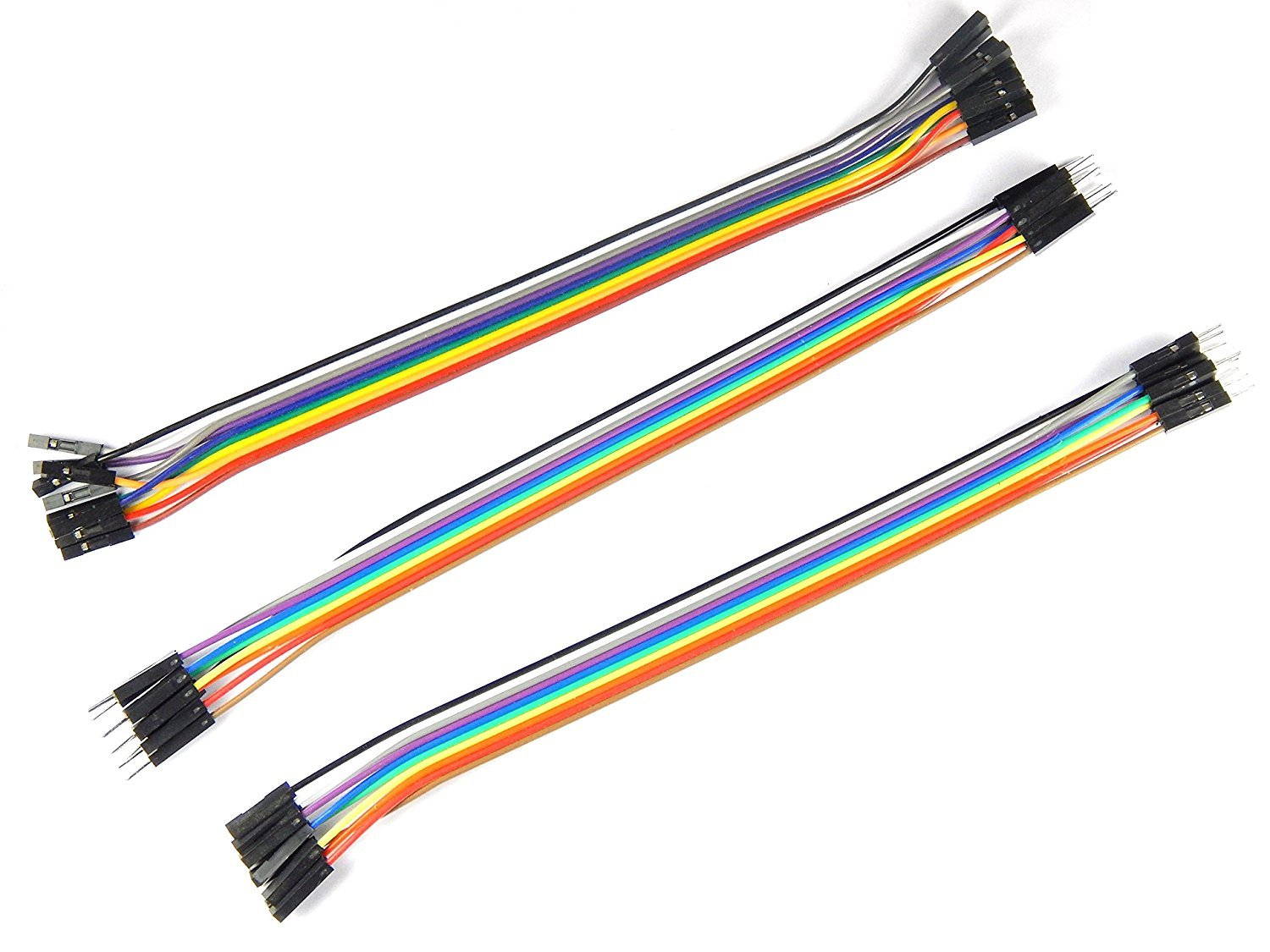
- 9 male to female jumper cables
- 1 pin oscillocope probe
- 2 banana-banana power cables
- 1 multimeter with sharp termination cables
- 1 power supply
- 1 Signal generator (10 MHz - 8 GHz)
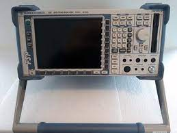
- 1 Spectrum Analyser (up to 25 GHz)
- 1 SMA DC block
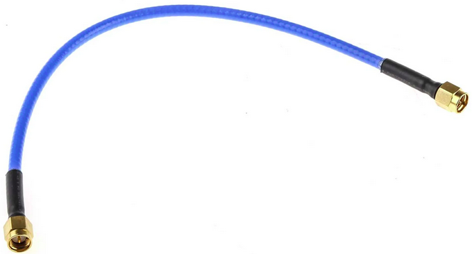
- 2 SMA to SMA 50 ohm coaxial cables
- 2 SMA to U.FL header transition
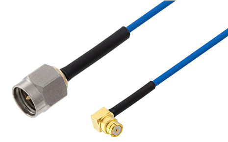
- 2 SMA to MS156 probe transition
- 1 OBC board with at least the STM and pull up resistors soldered OR a Nucleo board + PC with SMT32Cube IDE + USB to mini USB cable
Below is the connections schematic:
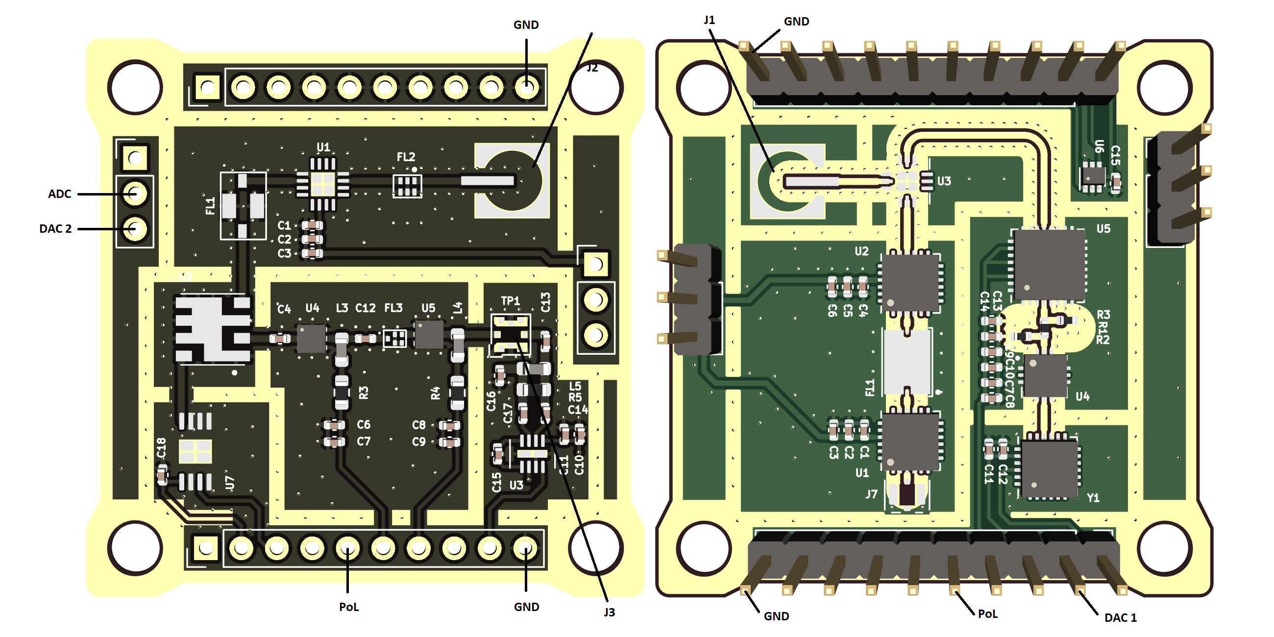
Make connections
- Turn on equipment
- Spectrum analizer
- Signal generator
- Power supply
-
Configure to desired parameters
- Spectrum analizer
- Set center frequency
- Set enough span
- Set RBW and VBW to an adecuate level
- Power supply
- Set Voltage to 3.3V
- Set current limit to 0.3A
- Spectrum analizer
-
Set up nucleo board and PC
- Make sure the proper code is loaded into the nucleo board
- Connect the power supply to the payload:
- Vcc to PoL
- GND to GND
- Connect the DAC output to the DAC 1
- Connect the ADC input to the ADC_Out
- Connect the signal generator output to the IF input PIN
- Connect the spectrum analizer to the switched measuring pin
- Connect PC to ground (plug in the charger).
- Connect necleo board to computer by USB.
Pass/Fail Criteria
This test will be considered passed if all of the following actions are performed succesfully:
- The code executes correctly upon flashing.
- A 1 GHz band noise-level sweep centered at 24.5 GHz is correctly filtered, amplified, downconverted to 869 Mhz within a 16 MHz bandwidth at -6dB.
- The resulted signal is translated by the RSSI into the appropiate voltage according to the manufacturer's specifications.
- The data aquisition process is correctly performed with the data being accessible from the STM32's flash memory banks.
- The system detects correctly certain RF signalssed detection is yet to be completely characterized.
The signals inputed and their supposed detection is yet to be completely characterized.
Test Plan (By Subblocks)
Before moving towards the testing of the whole subsystem, in order to single out possible errors, the payload's isolated segments will be tested a part, starting for simplicity with those which do not require a STM32 (be it a Nucleo Board or the OBC&COMMS board) to be verified.
RF chain Low Noise Amplifier (LNA)
In the form of the HMC342, fully explained in the appropiate P/L page, under the ³Cat-NXT Design chapter, the LNA is supposed to provide a gain of arround 19dB (at 24-25 GHz) over the Ka-band. To test this feature, a signal will be introduced at the receiver's input, and sampled from the first RF chain probe. The procedure is as follows:
-
First of all, the board should be operational. This can be checked by having a current consumption of cca 230 mA seen on the power supply display and with a voltage between 3.1 V and 3.3 V measured between the P/L_Power and GND pins. If otherwise, repeat the previous sub-section steps.
-
Connect the signal generator output through the SMA-U.FL termination to the J1 coaxial header input connector.
-
Attach pin probe termination to the free end of the coaxial cable of the spectrum analyser and connect it to the output pin of the LNA.
-
Set up the spectrum analyser to a center frequency of 24.5 GHz, a span of 2 GHz (having a total observable window from 23.5 GHz to 25.5 GHz) and using the maxim Autopick setting for ease of interpretation.
-
With the board and LNA powered as detailed above, select a tone of -80 dBm in ampltude and 24.5 GHz of frequency on the signal generator and then enable its output.
-
Observe the reading on the spectrum analyser. The same tone inputted should be visible, but with an amplitude gain of cca 19 dB. Note down any frequency shift if the case and take screen captures as needed.
-
Repeat the last two steps, this time at a number of different frequencies from 24 GHz to 25 GHz. It is recommended to do so at 100 MHz apart.
-
If the gain observed along said measurements coincides with the values provided by the manufacturer within a 5% tolerance, this test is considered passed.
Bandpass filters
Once the LNA is proven to work fine, the filters mut be checked. For these operations the same procedure is followed.
-
Connect a 50 Ohm matching load to the SMA-U.FL termination to the J1 coaxial header input connector, the RF Input.
-
Attach a pin probe termination to the free end of the coaxial cable of the spectrum analyser and connect it to the output pin of the filter.
-
This step is detailed for each filter.
-
If the BW observed along said measurements coincides with the values provided by the manufacturer within a 5% tolerance, this test is considered passed.
Ka band filter
-
Set up the spectrum analyser to a center frequency of 24.5 GHz, a span of 2 GHz (having a total observable window from 23.5 GHz to 25.5 GHz).
- Meaure the observed BW at -3dB.
IF filtering
-
Set up the spectrum analyser to a center frequency of 7169 MHz, a span of 2 GHz.
- Meaure the observed BW at -3dB.
SAW filter
The B39871B4316P810 bandpass filter's function is to select the signal within a range indicated by the manufacturer to be between 862 MHz and 876MHz, with an insertion loss of lower than 1.6 dB in-band. These characteristics can be tested as follows:
-
Set up the spectrum analyser to a center frequency of 869 MHz, a span of 50 GHz.
- Meaure the observed BW at -3dB.
RF downconversion tuner
The downconversion of this receiver is done using the voltage controlled HMC260 tuner, from the 24-25 GHz RF chain to the 7 GHz IF chain, by applying a frequency sweep. The steps to follow are:
-
Make sure that the configuration from the Set-Up section is in place.
-
Verify that the OBC PoL is turned on and the DAC pin holds a voltage constant controllable voltage.
-
Connect the signal generator output through the SMA-U.FL termination to the J1 coaxial header input connector.
-
Attach a SMA-U.FL probe termination to the free end of the coaxial cable of the spectrum analyser and connect it to the J2 U.FL coaxial header, the IF input terminal.
-
Set up the spectrum analyser to a center frequency of 24.5 GHz, a span of 2 GHz (having a total observable window from 23.5 GHz to 25.5 GHz) and using the maxim Autopick setting for ease of interpretation.
-
With the board powered as detailed above, select a tone of -80 dBm in ampltude and 24.5 GHz of frequency on the signal generator and then enable its output.
-
Observe the reading on the spectrum analyser. The same tone inputted should be visible, but with an amplitude loss of 9 to 12 dB. More importantly, the frequency shift must be the one according to the inputed voltage.
Note that the relation between voltage and frequency is not linear and need to be characterized as stated in the VCO calibration procedure
-
Repeat the last two steps, this time at a number of different frequencies from 24 GHz to 25 GHz. It is recommended to do so at 100 MHz apart.
-
If the attenuation and frequency shift observed along said measurements coincides with the values provided by the manufacturer within a 5% tolerance, this test is considered passed.
IF downconversion tuner
The downconversion of this receiver is done using the voltage controlled SIM-14+ tuner, from the 6669-7669 MHz IF chain to the 869 MHz LF chain, by applying a frequency sweep. The steps to follow are:
-
Make sure that the configuration from the Set-Up section is in place.
-
Verify that the OBC PoL is turned on and the DAC pin holds a voltage constant controllable voltage.
-
Connect the signal generator output through the SMA-U.FL termination to the J1 coaxial header input connector.
-
Attach a SMA-U.FL probe termination to the free end of the coaxial cable of the spectrum analyser and connect it to the J3 U.FL coaxial header, the IF input terminal.
-
Set up the spectrum analyser to a center frequency of 7169 MHz, a span of 2 GHz, and using the maxim Autopick setting for ease of interpretation.
-
With the board powered as detailed above, select a tone of -80 dBm in ampltude and 7169 MHz of frequency on the signal generator and then enable its output.
-
Observe the reading on the spectrum analyser. The same tone inputted should be visible, but with an amplitude loss of 6.7 to 9.5 dB. More importantly, the frequency shift must be the one according to the inputed voltage.
Note that the relation between voltage and frequency is not linear and need to be characterized as stated in the VCO calibration procedure
-
Repeat the last two steps, this time at a number of different frequencies from 24 GHz to 25 GHz. It is recommended to do so at 100 MHz apart.
- Repeat the last three steps, this time at a number of different VCO voltages from 0 to 3 V. It is recommended to do so at 100mV apart.
-
If the attenuation and frequency shift observed along said measurements coincides with the values provided by the manufacturer within a 5% tolerance, this test is considered passed.
Test Plan (Full subsystem)
From this point the document is a stub.
Having tested and isolated possible errors as much as possible in a bit-by-bit manner in the previous section, a full subsystem test will now be performed.
-
Make sure that the configuration from the Set-Up section is in place as well as the OBC PoL is turned on.
-
Connect the signal generator output through the SMA-U.FL termination to the J1 coaxial header. It is recommended that at least the first full SSV is done by way of signal generator input, with later tests possibly replacing this input with the real one by way of the antenna in order to firstly test the front end separate from any possible errors.
-
Configure the signal generator to output a 24 GHz - 25 GHz frequency sweep of -100 dBm amplitude with random spikes at -80 dBm and enable its output.
-
Using the IDE, initiate the P/L task within the STM32, using the full PQ firmware scheduler.
-
Using the Umbilical connection, download the flash memory experiment files
7. Test Results
8. Anomalies
9. Conclusions
RFI-5G FE-Top SSV
Document Scope
The objective of this document is to detail the procedures, results and conclusions to properly test at subsystem level the RFI-5G front-end top board. Several parts will be tested:
- Test of the LNA chain
- Test of the LO chain
- Test of the Front-End top board RF
- Test of the temperature sensor
Test of the LNA chain
Test Description and Objectives
The purpose of this test is to validate that the HMC342 LNA amplifier provides the expected +19 dB of gain for input signals between 24 to 25 GHz, and that the band-pass filter does not introduce more than the expected -4 dB of losses.
Since the probing used is not the frequency range used, this is only a qualitative test to check if the LNA is providing gain and validate that the consumption is nominal.
Requirements Verification
This test does not verify any requirement, and is only to check that the board part works as expected.
Test Set-Up
The required components for this test are the following:
| RFI-5G front-end top board |
|
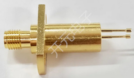
| C.FL to SMA-2.92mm adapter |
|
| C.FL cable |
|
| RF probe |
|
| SMA 50 Ohm RF load |
|
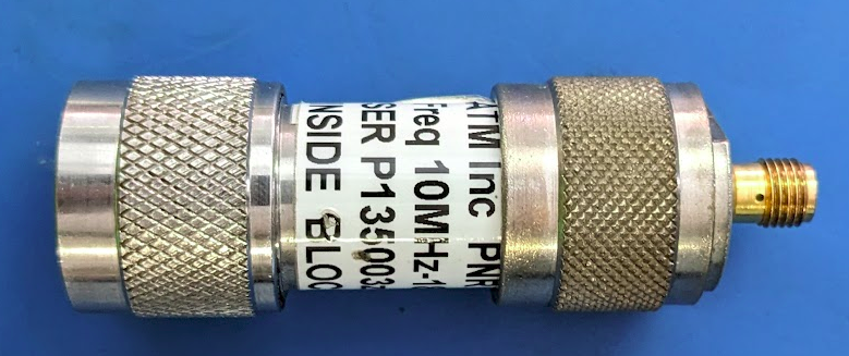
| DC Block N to SMA adapter |
|
| Power supply |
|
| Signal Generator capable of at least 25 GHz |
|
| Spectrum Analyzer capable of at least 25 GHz |
|
| 2x Jumper cables |
|
| 2x Banana cables |
|
| 2x Crocodrile clips |
|
| 2x SMA 2.92 mm cables |
|
| SMA to SMP cable |
|


The steps to prepare the setup are the following:
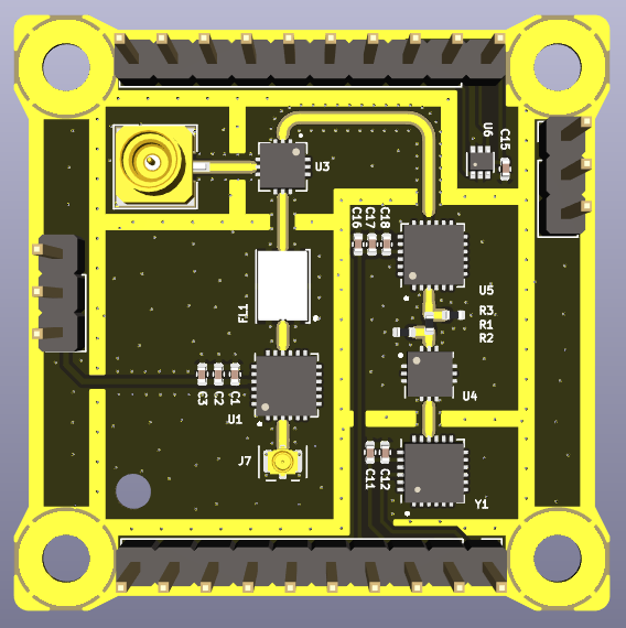
- Connect the output from the signal generator to the antenna input of the RFI-5G front-end top board by using the C.FL cable and the C.FL to 2.92 mm adapter.
- Connect the power supply to the Vcc_LNA1 and GND pins with the jumper cables and the crocodile clips.
- Connect the DC-block N to SMA adapter to the spectrum analyzer input.
- Connect the RF probe to the spectrum analyzer using one SMA cable.
- Connect the SMA 50 Ohm RF load to the output of the mixer with the SMA to SMP cable.
The diagram below represents the initial setup:

Pass/Fail Criteria
The test will be considered successful if the LNA shows to provide gain (~19 dB) and the power consumption matches the expected one (~43 mA at 3.3 V). There is though some margin accepted, since the RF probe and cables are not rated for the frequency range used.
Test Plan
|
Step ID |
Description |
Pass/Fail Criteria |
Actual |
Passed [Y/N] |
| RFI-5G-TOP-LNA-000 |
Make sure that the power supply and signal generator outputs are off. | Passes if power supply and signal generator outputs are off. |
||
| RFI-5G-TOP-LNA-010 |
Prepare the setup as stated in 2.3. |
Passes if setup prepared. |
||
| RFI-5G-TOP-LNA-020 |
Set the power supply to 3 V and limit the current to 60 mA. |
Passes if power supply set. |
||
| RFI-5G-TOP-LNA-030 |
Set the signal generator to: f = 24.5 GHz Pout = -70 dBm |
Passes if signal generator set. |
||
| RFI-5G-TOP-LNA-040 |
Set the spectrum analyzer to: f = 24.5 GHz Span = 10 MHz RBW = 10 kHz VBW = 1 kHz Trace = Max Hold |
Passes if spectrum analyzer set. |
||
| RFI-5G-TOP-LNA-050 |
Switch on the signal generator output. |
Passes if signal generator output is on. |
||
| RFI-5G-TOP-LNA-060 |
Switch on the power supply. If the power supply is limiting switch it off immediately. |
Passes if power supply is on and not current limiting. |
||
| RFI-5G-TOP-LNA-070 |
Note the voltage and current. If the current consumption is abnormal switch it off immediately. |
Passes if voltage and current are within specification (some margin is allowed but has to be explained why). |
Voltage: Current: |
|
| RFI-5G-TOP-LNA-080 |
With the RF probe, probe the input of the LNA by carefully touching with the signal pogo-pin the RF input pin of the LNA. |
Passes if a signal is shown in the spectrum analyzer. |
||
| RFI-5G-TOP-LNA-090 | Set the trace mode in the spectrum analyzer to VIEW to freeze the image. |
Passes if trace mode is VIEW. |
||
|
RFI-5G-TOP-LNA-100 |
Add a second trace in the spectrum analyzer with the same configuration as the first one. |
Passes if spectrum analyzer set. |
||
| RFI-5G-TOP-LNA-110 | With the RF probe, probe the output of the LNA by carefully touching with the signal pogo-pin the RF output pin of the LNA. |
Passes if a signal is shown in the spectrum analyzer. | ||
| RFI-5G-TOP-LNA-120 | Set the trace mode in the spectrum analyzer to VIEW to freeze the image. |
Passes if trace mode is VIEW. |
||
| RFI-5G-TOP-LNA-130 |
Add one marker to the peak of trace 1, and another marker that measures the delta in the peak of trace 2. Note the gain and frequency delta values. |
Passes if the gain is within specification (some margin is allowed but has to be explained why). |
Gain: Frequency: |
|
| RFI-5G-TOP-LNA-140 |
Capture the screen of the spectrum analyzer and save it into a USB drive. |
Passes if .wmf is saved into a USB drive. |
File name: |
|
| RFI-5G-TOP-LNA-150 |
Add a third trace in the spectrum analyzer with the same configuration as the first one. |
Passes if spectrum analyzer set. |
||
| RFI-5G-TOP-LNA-160 | With the RF probe, probe the output of the band-pass filter by carefully touching with the signal pogo-pin the RF output pin of the filter. | Passes if the gain is within specification (some margin is allowed but has to be explained why). | ||
| RFI-5G-TOP-LNA-170 | Set the trace mode in the spectrum analyzer to VIEW to freeze the image. |
Passes if trace mode is VIEW. |
||
| RFI-5G-TOP-LNA-180 |
Add a third marker in trace 3. Note the power and frequency delta values with marker 1. |
Passes if the gain is within specification (some margin is allowed but has to be explained why). |
Gain: Frequency: |
|
| RFI-5G-TOP-LNA-190 |
Capture the screen of the spectrum analyzer and save it into a USB drive. |
Passes if .wmf is saved into a USB drive. |
File name: |
|
| RFI-5G-TOP-LNA-200 |
Switch off the power supply and the signal generator. |
Passes if power supply and signal generator are off. |
||
| RFI-5G-TOP-LNA-210 |
If all steps are passed, proceed with next test. |
Passes if all steps passed. |
Test Results
Description of the Test results with supporting data.
- Test name, test execution dates, the test facility used and the operators
- Test Logbooks
- “As-run” procedures (to be provided in annex)
- Test facility results (if applicable)
- Photographs relevant to the set-up(s) and inspection(s) (may also be added in the Conclusions to clarify a close-out judgement, e.g. for an inspection)
- Analysis of the test data and relevant assessment.
- Synthesis of the overall test results per verification (e.g. Vibration, Inspection 1, Inspection 2, etc.).
Anomalies
List of deviations to the Test Specification and Procedure and non-conformances witnessed during the test campaign, including a brief description, the close-out status and reference to the relevant reports.
Conclusions
The Conclusions shall include (where needed as annex):
- Test results, including as a minimum:
- Requirement to be verified
- Subsections of test campaign in which that requirement was verified (e.g. Thermal Vacuum RFT 1, Inspection 1, Inspection 2, ...)
- Close-out judgement (compliance status) and rationale, per subsection of the test
- Traceability to used documentation
- Conformance or deviation including references
- Overall conclusion on the success of the test, including clearly stated and described open issues and possible remediating actions.
- Test Readiness Review minutes and Post Test Review minutes
Test of the LO chain
Test Description and Objectives
The purpose of this test is to validate that the LO chain works as intended. This means that the HMC506 VCO provides a tone at the expected 8665.5 MHz, and that the HMC342 LO amplifier provides gain (~19 dB) so that the LO input of the mixer is over 12 dBm (~14 dBm).
Since the probing used is not the frequency range used, this is only a qualitative test to check if the LO chain is providing the correct LO tone to the mixer and that the consumption is nominal.
Requirements Verification
This test does not verify any requirement, and is only to check that the board part works as expected.
Test Set-Up
The required components for this test are the following:
| RFI-5G front-end top board |
|
| C.FL to SMA-2.92mm adapter |
|
| C.FL cable |
|
| RF probe |
|
| SMA 50 Ohm RF load |
|
| DC Block N to SMA adapter |
|
| Power supply |
|
| Spectrum Analyzer capable of at least 25 GHz |
|
| 6x Jumper cables |
|
| 6x Banana cables |
|
| 6x Crocodrile clips |
|
| 2x SMA 2.92 mm cables |
|
| SMA to SMP cable |
|
The steps to prepare the setup are the following:
- Connect the output from the signal generator to the antenna input of the RFI-5G front-end top board by using the C.FL cable and the C.FL to 2.92 mm adapter.
- Connect the first channel of the power supply to the Vcc_VCO and GND pins with the jumper cables and the crocodile clips.
- Connect the second channel of the power supply to the Vtune1 and GND pins with the jumper cables and the crocodile clips.
-
Connect the third channel of the power supply to the
and GND pins with the jumper cables and the crocodile clips.Vcc_IF1AmpVcc_LO1Amp - Connect the DC-block N to SMA adapter to the spectrum analyzer input.
- Connect the RF probe to the spectrum analyzer using one SMA cable.
- Connect the SMA 50 Ohm RF load to the output of the mixer with the SMA to SMP cable.
The diagram below represents the initial setup:

Pass/Fail Criteria
The test will be considered successful if the LO shows a tone at 8665.5 MHz +- 5%, if the LO amplifier provides the expected gain (~19 dB) and if the level of the LO input of the mixer is over 10 dBm. Additionally, the current consumption has to be nominal.
Test Plan
|
Step ID |
Description |
Pass/Fail Criteria |
Actual |
Passed [Y/N] |
| RFI-5G-TOP-LO-000 |
Make sure that the power supply is off. |
Passes if power supply and signal generator outputs are off. |
||
| RFI-5G-TOP-LO-010 |
Prepare the setup as stated in 3.3. |
Passes if setup prepared. |
||
| RFI-5G-TOP-LO-020 |
Set the first channel of the power supply to 3 V and limit the current to 100 mA. |
Passes if power supply set. |
||
| RFI-5G-TOP-LO-030 |
Set the second channel of the power supply to 8.7 V and limit the current to 10 mA. |
Passes if power supply set. |
||
| RFI-5G-TOP-LO-040 | Set the third channel of the power supply to 3 V and limit the current to 60 mA. |
Passes if power supply set. |
||
| RFI-5G-TOP-LO-050 |
Set the spectrum analyzer to: f = 8665.5 MHz Span = 100 MHz RBW = 100 kHz VBW = 3 kHz Trace = Clear/Write |
Passes if spectrum analyzer set. |
||
| RFI-5G-TOP-LO-060 |
Switch on the first channel of the power supply. If the power supply is limiting switch it off immediately. |
Passes if power supply is on and not current limiting. |
||
| RFI-5G-TOP-LO-070 |
Switch on the |
Passes if power supply is on and not current limiting. |
||
| RFI-5G-TOP-LO-080 |
Note the voltage and current. If the current consumption is abnormal switch it off immediately. |
Passes if voltage and current are within specification (some margin is allowed but has to be explained why) |
CH1 Voltage: Current: CH2 Voltage: Current: |
|
| RFI-5G-TOP-LO-080 |
With the RF probe, probe the output of the VCO by carefully touching with the signal pogo-pin the RF output pin of the LNA. |
Passes if a signal is shown in the spectrum analyzer. |
||
| RFI-5G-TOP-LO-090 | Adjust the Vtune1 voltage until the LO frequency is centered to the desired 8665.5 MHz. |
Passes if LO frequency is ~8665.5 MHz. |
CH2 Voltage: frequency: |
|
| RFI-5G-TOP-LO-100 | Set the trace mode in the spectrum analyzer to VIEW to freeze the image. |
Passes if trace mode is VIEW. |
||
| RFI-5G-TOP-LO-110 | Capture the screen of the spectrum analyzer and save it into a USB drive. |
Passes if .wmf is saved into a USB drive. |
File name: |
|
| RFI-5G-TOP-LO-120 | Set the trace mode in the spectrum analyzer to CLEAR/WRITE to clear the spectrum. |
Passes if trace mode is CLEAR/WRITE. | ||
|
RFI-5G-TOP-LO-130 |
Set the spectrum analyzer to: f = 17331 MHz Span = 200 MHz RBW = 100 kHz VBW = 3 kHz Reference level = 10 dBm Trace = Max Hold |
Passes if spectrum analyzer set. |
||
| RFI-5G-TOP-LO-140 | With the RF probe, probe the output of the frequency multiplier by carefully touching with the signal pogo-pin the RF output pin of the frequency multiplier. |
Passes if a signal is shown in the spectrum analyzer. | ||
| RFI-5G-TOP-LO-150 | Set the trace mode in the spectrum analyzer to VIEW to freeze the image. |
Passes if trace mode is VIEW. |
||
| RFI-5G-TOP-LO-160 |
Add one marker at the peak. Note the power and frequency values. | Passes if power and frequency are within specification. |
Power: Frequency: |
|
| RFI-5G-TOP-LO-170 |
Add a second trace in the spectrum analyzer with the same configuration as the first one. | Passes if spectrum analyzer set. | ||
| RFI-5G-TOP-LO-180 |
Switch on the third channel of the power supply. If the power supply is limiting switch it off immediately. |
Passes if power supply is on and not current limiting. |
||
| RFI-5G-TOP-LO-190 | Note the voltage and current. If the current consumption is abnormal switch it off immediately. |
Passes if voltage and current are within specification (some margin is allowed but has to be explained why) |
CH3 Voltage: Current: |
|
| RFI-5G-TOP-LO-200 |
With the RF probe, probe the output of the LO amplifier by carefully touching with the signal pogo-pin the RF output pin of the LO amplifier. |
Passes if a signal is shown in the spectrum analyzer. | ||
| RFI-5G-TOP-LO-210 | Set the trace mode in the spectrum analyzer to VIEW to freeze the image. |
Passes if trace mode is VIEW. |
||
| RFI-5G-TOP-LO-220 | Add one marker to the peak of trace 1, and another marker that measures the delta in the peak of trace 2. Note the power and frequency delta values. |
Passes if the gain is within specification (some margin is allowed but has to be explained why). |
Power: Frequency: |
|
| RFI-5G-TOP-LO-230 | Capture the screen of the spectrum analyzer and save it into a USB drive. |
Passes if .wmf is saved into a USB drive. |
File name: |
|
| RFI-5G-TOP-LO-240 | Switch off the power supply and the signal generator. |
Passes if power supply and signal generator are off. |
||
| RFI-5G-TOP-LO-250 | If all steps are passed, proceed with next test. |
Passes if all steps passed. |
Test Results
Description of the Test results with supporting data.
- Test name, test execution dates, the test facility used and the operators
- Test Logbooks
- “As-run” procedures (to be provided in annex)
- Test facility results (if applicable)
- Photographs relevant to the set-up(s) and inspection(s) (may also be added in the Conclusions to clarify a close-out judgement, e.g. for an inspection)
- Analysis of the test data and relevant assessment.
- Synthesis of the overall test results per verification (e.g. Vibration, Inspection 1, Inspection 2, etc.).
Anomalies
List of deviations to the Test Specification and Procedure and non-conformances witnessed during the test campaign, including a brief description, the close-out status and reference to the relevant reports.
Conclusions
The Conclusions shall include (where needed as annex):
- Test results, including as a minimum:
- Requirement to be verified
- Subsections of test campaign in which that requirement was verified (e.g. Thermal Vacuum RFT 1, Inspection 1, Inspection 2, ...)
- Close-out judgement (compliance status) and rationale, per subsection of the test
- Traceability to used documentation
- Conformance or deviation including references
- Overall conclusion on the success of the test, including clearly stated and described open issues and possible remediating actions.
- Test Readiness Review minutes and Post Test Review minutes
Test of the Front-end Top board RF
Test Description and Objectives
The purpose of this test is to validate the correct functioning of the RF part of the RFI-5G front-end top, i.e., with an input signal between 24-25 GHz, the signal is down-converted to an intermediate signal with frequency between 6669-76669 MHz, with a net gain of 5 dB.
Requirements Verification
This test does not verify any requirement, and is only to check that the board part works as expected.
Test Set-Up
The required components for this test are the following:
| RFI-5G front-end top board |
|
| RFI-5G interface board with inverse connectors |
|
| C.FL to SMA-2.92mm adapter |
|
| C.FL cable |
|
| DC Block N to SMA adapter |
|
| Power supply |
|
| Signal Generator capable of at least 25 GHz |
|
| Spectrum Analyzer capable of at least 25 GHz |
|
| 2x Banana cables |
|
| SMA 2.92 mm cables |
|
| SMA to SMP cable |
|
The steps to prepare the setup are the following:
- Mate the RFI-5G front-end top board with the RFI-5G interface board that has the inverse pin header.
- Connect the EGSE to the power supply with the banana cables.
- Connect the output from the signal generator to the antenna input of the RFI-5G front-end top board by using the C.FL cable and the C.FL to 2.92 mm adapter.
- Connect the DC-block N to SMA adapter to the spectrum analyzer input.
- Connect the RFI-5G front-end top board output to the spectrum analyzer using the SMA to SMP cable.
The diagram below represents the initial setup:

Pass/Fail Criteria
The test will be considered successful if the output of the RFI-5G front-end top board is a signal between 6669-7669 MHz when the antenna input is between 24-25 GHz, and the board provides a net gain of +5 dB. Additionally, the current consumption has to be nominal.
Test Plan
|
Step ID |
Description |
Pass/Fail Criteria |
Actual |
Passed [Y/N] |
| RFI-5G-TOP-RF-000 |
Make sure that the power supply and signal generator outputs are off. | Passes if power supply and signal generator outputs are off. |
||
| RFI-5G-TOP-RF-010 |
Prepare the setup as stated in 4.3. |
Passes if setup prepared. |
||
| RFI-5G-TOP-RF-020 |
Set the first channel of the power supply to 3.3 V and limit the current to 200 mA. |
Passes if power supply set. |
||
| RFI-5G-TOP-RF-030 |
Set the spectrum analyzer to: f = 7169 MHz Span = 200 MHz RBW = 100 kHz VBW = 3 kHz Reference level = -20 dBm Trace = Clear/Write |
Passes if spectrum analyzer set. |
||
| RFI-5G-TOP-RF-040 |
Set the signal generator to: f = 24.5 GHz Pout = -80 dBm |
Passes if signal generator set. | ||
| RFI-5G-TOP-RF-050 |
Switch on the first channel of the power supply. If the power supply is limiting switch it off immediately. |
Passes if power supply is on and not current limiting. |
||
| RFI-5G-TOP-RF-060 | Note the voltage and current. If the current consumption is abnormal switch it off immediately. |
Passes if voltage and current are within specification (some margin is allowed but has to be explained why). |
Voltage: Current: |
|
| RFI-5G-TOP-RF-070 | Enable the output of the signal generator. | Passes if signal generator output is enabled. | ||
| RFI-5G-TOP-RF-080 | Note the voltage and current. If the current consumption is abnormal switch it off immediately. |
Passes if voltage and current are same as in RFI-5G-TOP-RF-060. |
Voltage: Current: |
|
| RFI-5G-TOP-RF-090 | Add one marker at the peak. Note the frequency and power of the intermediate signal. Additionally compute the net gain and the frequency shift. | Passes if the net gain is +5 dB and the frequency shift of 17331 MHz. |
frequency = Power = frequency shift = Gain = |
|
| RFI-5G-TOP-RF-100 | Set the trace mode in the spectrum analyzer to VIEW to freeze the image. |
Passes if trace mode is VIEW. |
||
| RFI-5G-TOP-RF-110 | Capture the screen of the spectrum analyzer and save it into a USB drive. |
Passes if .wmf is saved into a USB drive. |
File name: |
|
| RFI-5G-TOP-RF-120 | Set the trace mode in the spectrum analyzer to CLEAR/WRITE to clear the spectrum. |
Passes if trace mode is CLEAR/WRITE. | ||
| RFI-5G-TOP-RF-130 |
Switch off the output of the signal generator. |
Passes if signal generator output is off. |
||
| RFI-5G-TOP-RF-140 |
Set the spectrum analyzer to: f = 7169 MHz Span = 1200 MHz RBW = 300 kHz VBW = 30 kHz Trace = Max Hold |
Passes if spectrum analyzer set. |
||
| RFI-5G-TOP-RF-150 |
Set the signal generator to: Mode = frequency sweep f = 24.5 GHz Span = 1 GHz Step = 10 MHz P = -80 dBm |
Passes if signal generator set. |
|
|
| RFI-5G-TOP-RF-160 |
Switch on the output of the signal generator. |
Passes if signal generator output is on. |
||
| RFI-5G-TOP-RF-170 | Wait until a complete frequency sweep is done. | Passes when complete frequency sweep finishes. | ||
| RFI-5G-TOP-RF-180 | Check qualitatively the flatness of the RFI-5G front-end top board RF output. | Passes if the RF output is "flat". | ||
| RFI-5G-TOP-RF-190 | Set the trace mode in the spectrum analyzer to VIEW to freeze the image. |
Passes if trace mode is VIEW. |
|
|
| RFI-5G-TOP-RF-200 | Capture the screen of the spectrum analyzer and save it into a USB drive. |
Passes if .wmf is saved into a USB drive. |
File name: |
|
| RFI-5G-TOP-RF-210 | Switch off the power supply and the signal generator. |
Passes if power supply and signal generator are off. |
||
| RFI-5G-TOP-RF-220 | If all steps are passed, proceed with next test. |
Passes if all steps passed. |
Test Results
Description of the Test results with supporting data.
- Test name, test execution dates, the test facility used and the operators
- Test Logbooks
- “As-run” procedures (to be provided in annex)
- Test facility results (if applicable)
- Photographs relevant to the set-up(s) and inspection(s) (may also be added in the Conclusions to clarify a close-out judgement, e.g. for an inspection)
- Analysis of the test data and relevant assessment.
- Synthesis of the overall test results per verification (e.g. Vibration, Inspection 1, Inspection 2, etc.).
Anomalies
List of deviations to the Test Specification and Procedure and non-conformances witnessed during the test campaign, including a brief description, the close-out status and reference to the relevant reports.
Conclusions
The Conclusions shall include (where needed as annex):
- Test results, including as a minimum:
- Requirement to be verified
- Subsections of test campaign in which that requirement was verified (e.g. Thermal Vacuum RFT 1, Inspection 1, Inspection 2, ...)
- Close-out judgement (compliance status) and rationale, per subsection of the test
- Traceability to used documentation
- Conformance or deviation including references
- Overall conclusion on the success of the test, including clearly stated and described open issues and possible remediating actions.
- Test Readiness Review minutes and Post Test Review minutes
Test of the temperature sensor
Test Description and Objectives
The purpose of this test is to validate the correct functioning of temperature sensor in the RFI-5G front-end top board, and that the sensor library code functions correctly.
Requirements Verification
This test does not verify any requirement, and is only to check that the board part works as expected.
Test Set-Up
The required components for this test are the following:
| RFI-5G front-end top board |
|
| RFI-5G interface board with inverse connectors |
|
| RFI-5G EGSE |
|
| STM32 Nucleo-L476RG board |
|
| USB A-to-mini cable |
|
| Power supply |
|
| 2x Banana cables |
|
| 2x Jumper cables |
|
| Temperature sensor test code |
NA |


The steps to prepare the setup are the following:
- Mate the RFI-5G front-end top board with the RFI-5G interface board that has the inverse pin header.
- Connect the EGSE to the power supply with the banana cables.
- Connect the output from the signal generator to the antenna input of the RFI-5G front-end top board by using the C.FL cable and the C.FL to 2.92 mm adapter.
- Connect the DC-block N to SMA adapter to the spectrum analyzer input.
- Connect the RFI-5G front-end top board output to the spectrum analyzer using the SMA to SMP cable.
The diagram below represents the initial setup:
Missing setup picture
Pass/Fail Criteria
Description of which metric is used to perform the test and when it is considered that the test passed or not. If different metrics are used, it is important to define when the test passed or not (e.g. when all the metrics are in the pass criteria, or when only one of them).
Test Plan
This section includes the test sequence necesary to do the test. The test sequence must include all the steps, from the set-up up to the conclusion of the test.
Test Results
Description of the Test results with supporting data.
- Test name, test execution dates, the test facility used and the operators
- Test Logbooks
- “As-run” procedures (to be provided in annex)
- Test facility results (if applicable)
- Photographs relevant to the set-up(s) and inspection(s) (may also be added in the Conclusions to clarify a close-out judgement, e.g. for an inspection)
- Analysis of the test data and relevant assessment.
- Synthesis of the overall test results per verification (e.g. Vibration, Inspection 1, Inspection 2, etc.).
Anomalies
List of deviations to the Test Specification and Procedure and non-conformances witnessed during the test campaign, including a brief description, the close-out status and reference to the relevant reports.
Conclusions
The Conclusions shall include (where needed as annex):
- Test results, including as a minimum:
- Requirement to be verified
- Subsections of test campaign in which that requirement was verified (e.g. Thermal Vacuum RFT 1, Inspection 1, Inspection 2, ...)
- Close-out judgement (compliance status) and rationale, per subsection of the test
- Traceability to used documentation
- Conformance or deviation including references
- Overall conclusion on the success of the test, including clearly stated and described open issues and possible remediating actions.
- Test Readiness Review minutes and Post Test Review minutes
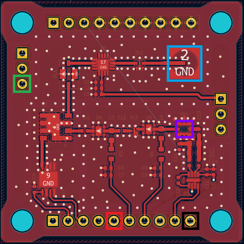
K-Band VCO Calibration Procedure
Objective
Measure the frequency response of the VCO and characterize it.
Steps to follow
-
Turn on equipment
- Spectrum analizer
- Power supply
-
Configure to desired parameters
- Spectrum analizer
- Set center frequency in the middle of VCO output band (6250MHz)
- Set span to match the VCO output band (1400MHz)
- Set RBW and VBW to an adecuate level
- Power supply
- Set Voltage to 3.3V
- Set current limit to 0.3A
- Spectrum analizer
-
Set up nucleo board and PC
- Make sure the proper code is loaded into the nucleo board
- Set up PuTTy
- Select the serial port terminal
- Set Speed(baud) to 115200
- Set data bits to 8
- Set stop bits to 1
- Turn off parity
- Set flow control to XON/XOFF
- Set COM port to the nucleo connected one
-
Make connections
- Connect the power supply to the payload:
- Vcc to PoL (RED)
- GND to GND (BLACK)
- Connect the DAC output to the DAC_In (GREEN)
- Connect the spectrum analizer to the switched measuring pin (PURPLE)

- Connect PC to ground (plug in the charger)
- Connect necleo board to computer by USB
- Connect the power supply to the payload:
-
Power on power supply
-
Begin the measurements procedure
- Enter frequency in PuTTy (begin on 5600 MHz)
- Measure where the input signal peak is and annotate it
- Annotate the deviation observed
- Repeat these steps with Fvco += 50 MHz
-
Update the VCO calibration and check it. If it’s not correct repeat the previous step
Front-end Gain calibration Procedure
Objective
Measure the total system gain at the output of the RSSI and equalize it.
Steps to follow
-
Turn on equipment
- Spectrum analizer
- Power supply
-
Configure to desired parameters
- Spectrum analizer
- Set center frequency in the middle of VCO output band (6250MHz)
- Set span to match the VCO output band (1400MHz)
- Set RBW and VBW to an adecuate level
- Power supply
- Set Voltage to 3.3V
- Set current limit to 0.3A
- Spectrum analizer
-
Set up nucleo board and PC
- Make sure the proper code is loaded into the nucleo board
-
- Connect the power supply to the payload:
- Vcc to PoL (RED)
- GND to GND (BLACK)
- Connect the DAC output to the DAC_In (GREEN)
- Connect the ADC input to the ADC_Out
- Load the IF Input with a 50 Ohm perfectly matched load.
- Connect the spectrum analizer to the switched measuring pin (PURPLE)
Make connections
- Connect PC to ground (plug in the charger)
- Connect necleo board to computer by USB
- Connect the power supply to the payload:
-
Power on power supply
-
Begin the measurements procedure
- Run the flashed program in Debug mode
- Once the program stops at the breakpoint, collect the calculated mean and plot it in a data processing software like Matlab.
-
Realize the calibration
- Calculate the mean of the collected data and substract it from each frequency bin mean. This will be the deviation.
- Extract the trend line from the deviation.
- Subtract trend line function from the received RSSI value. This will be the calibrated measurement.
-
Reboot the program and check if the equalization is now correct. If it’s not correct repeat the previous step
K-band Noise floor characterization Procedure
Objective
Measure the RSSI obtained though all the 1GHz band with only noise and characterize it.
Steps to follow
-
Turn on equipment
- Spectrum analizer
- Power supply
-
Configure to desired parameters
- Spectrum analizer
- Set center frequency in the middle of RSSI input band (869MHz)
- Set enough span to observe the RSSI input band (30MHz)
- Set RBW and VBW to an adecuate level
- Power supply
- Set Voltage to 3.3V
- Set current limit to 0.3A
- Spectrum analizer
-
Set up nucleo board and PC
- Make sure the proper code is loaded into the nucleo board
-
Make connections
- Connect the power supply to the payload:
- Vcc to PoL (RED)
- GND to GND (BLACK)
- Connect the DAC output to the DAC_In (GREEN)
- Connect the ADC input to the ADC_Out
- Load the IF Input with a 50 Ohm perfectly matched load.
- Connect the spectrum analizer to the switched measuring pin (PURPLE)
- Connect PC to ground (plug in the charger).
- Connect necleo board to computer by USB.
- Connect the power supply to the payload:
-
Power on power supply.
-
Begin the measurements procedure
- Run the flashed program in Debug mode.
- Measure the signal observed with the spectrum analyzer.
- Disconnect the spectrum analizer connected to the switched measuring pin (PURPLE).
- Once the program stops at the breakpoint, collect the calculated mean and plot it in a data processing software like Matlab.
-
Analyze the collected data.
K-band CW characterization Procedure
Objective
Measure the RSSI obtained though all the 1GHz band when inputting a CW and characterize it.
Steps to follow
-
Turn on equipment
- Spectrum analizer
- Signal generator
- Power supply
-
Configure to desired parameters
- Spectrum analizer
- Set center frequency in the middle of RSSI input band (869MHz)
- Set enough span to observe the RSSI input band (30MHz)
- Set RBW and VBW to an adecuate level
- Power supply
- Set Voltage to 3.3V
- Set current limit to 0.3A
- Spectrum analizer
-
Set up nucleo board and PC
- Make sure the proper code is loaded into the nucleo board
-
Make connections
- Connect the power supply to the payload:
- Vcc to PoL (RED)
- GND to GND (BLACK)
- Connect the DAC output to the DAC_In (GREEN)
- Connect the ADC input to the ADC_Out
- Connect the signal generator output to the IF input PIN (BLUE)
- Connect the spectrum analizer to the switched measuring pin (PURPLE)
- Connect PC to ground (plug in the charger).
- Connect necleo board to computer by USB.
- Connect the power supply to the payload:
-
Power on power supply.
-
Begin the measurements procedure
- Run the flashed program in Debug mode.
- Measure the signal observed with the spectrum analyzer.
- Disconnect the spectrum analizer connected to the switched measuring pin (PURPLE).
- Once the program stops at the breakpoint, collect the calculated mean and plot it in a data processing software like Matlab.
-
Analyze the collected data.
P/L3 Envelope Detection characterization Procedure
Objective
Characterize the capacity of the RFI Monitoring system to detect signals by Envelope Detection method.
Steps to follow
-
Turn on equipment
- Power supply
- Signal generator
-
Configure to desired parameters
- Power supply
- Set Voltage to 3.3V
- Set current limit to 0.3A
- Signal generator
- Set output frequency to some IF Band frequency
- Power supply
-
Set up nucleo board and PC
- Make sure the proper code is loaded into the nucleo board
-
Make connections
- Connect the power supply to the payload:
- Vcc to PoL (RED)
- GND to GND (BLACK)
- Connect the DAC output to the DAC_In (GREEN)
- Connect the ADC input to the ADC_Out
- Load the IF Input with a 50 Ohm perfectly matched load.
- Connect PC to ground (plug in the charger).
- Connect necleo board to computer by USB.
- Connect the power supply to the payload:
-
Power on power supply.
-
Begin the measurements procedure
- Run the flashed program in Debug mode.
- Once the program stops at the breakpoint, collect the calculated mean and plot it in a data processing software like Matlab.
-
Analyze the collected data.
P/L3 Statistical pulsed signal characterization Procedure
Objectives
Characterize the capacity of the RFI Monitoring system to detect pulsed signals by statistical algorithms.
Steps to follow
-
Turn on equipment
- Power supply
- Signal generator
-
Configure to desired parameters
- Power supply
- Set Voltage to 3.3V
- Set current limit to 0.3A
- Signal generator
- Set output frequency to some IF Band frequency periodic pulsed signals
- Power supply
-
Set up nucleo board and PC
- Make sure the proper code is loaded into the nucleo board
-
Make connections
- Connect the power supply to the payload:
- Vcc to PoL (RED)
- GND to GND (BLACK)
- Connect the DAC output to the DAC_In (GREEN)
- Connect the ADC input to the ADC_Out
- Load the IF Input with a 50 Ohm perfectly matched load.

- Connect PC to ground (plug in the charger).
- Connect necleo board to computer by USB.
- Connect the power supply to the payload:
-
Power on power supply.
-
Begin the measurements procedure
- Run the flashed program in Debug mode.
- Once the program stops at the breakpoint, collect the calculated mean and plot it in a data processing software like Matlab.
-
Analyze the collected data.